

Page 1
TSA1201
12-BIT, 50MSPS, 150mW A/D CONVERTER
■ 0.5Msps to 50Msps sampling frequency
■ 40mW @5Msps, 150mW @ 50Msps
■ 2.5V supply voltage with 2.5V/3.3V compati-
bility for digital I/O
■ Input range: 2Vpp differential
■ SFDR up to 77dB @ 50Msps, Fin=15MHz
■ ENOB up to10.5 bits @ 50Msps, Fin=15MHz
■ Built-in reference voltage with external bias
capability
■ Pinout compatibility with TSA0801, TSA1001
and TSA1002
DESCRIPTION
The TSA1201 is a 12-bit, 50MHz maximum
sampling frequency Analog to Digital converter
using a CMOS technology combining high
performances and very low power consumption.
The TSA1201 is based on a pipeline structure and
digital error correction to provide excellent static
linearity and achieve 10.5 effective bits at
Fs=50Msps, and Fin=15M Hz, with a global power
consumption of 150mW.
The TSA1201 features adaptative behaviour to
the application. Its architecture allows to sample
from 0.5Msps up to 50Msps, with a programmable
power consumption which makes the application
board even more optimized.
It integrates a proprietary track-and-hold structure
to ensure an high analog bandwidth of 1GHz and
enable IF-sampling.
Several features are available on the device. A
voltage reference is integrated in the circuit.
Differential or single-ended analog inputs can be
applied. The output data can be coded into two
differential formats. A Data Ready signal is raised
as the data is valid on the output and can be used
for synchronization purposes.
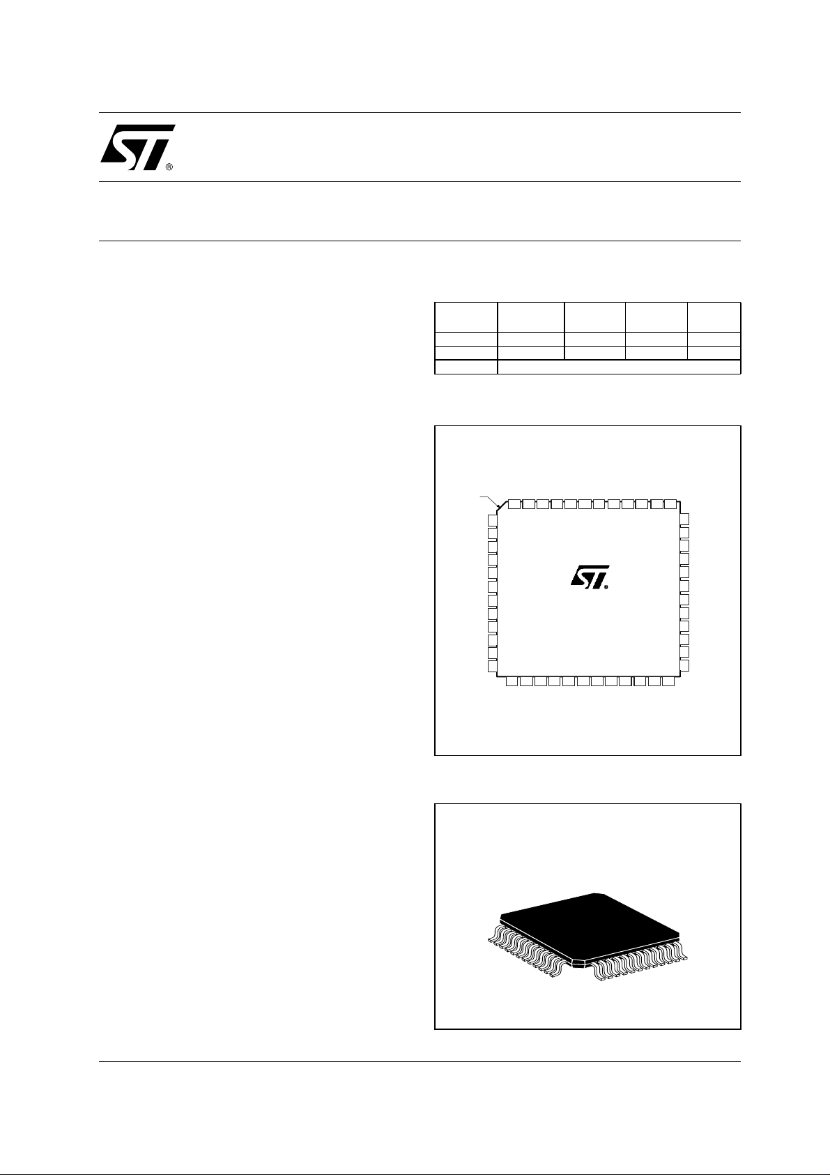
The TSA1201 is available in extended (-40°C to
+85°C) temperature range, in small 48 pins TQFP
package.
ORDER CODE
Part Number
TSA1201IF -40°C to +85°C TQFP48 Tray SA120 1I
TSA1201IFT -40°C to +85°C TQFP48 Tape & Reel SA1201I
EVAL1201/AA Evaluation board
Temperature
Range
Package Conditioning Marking
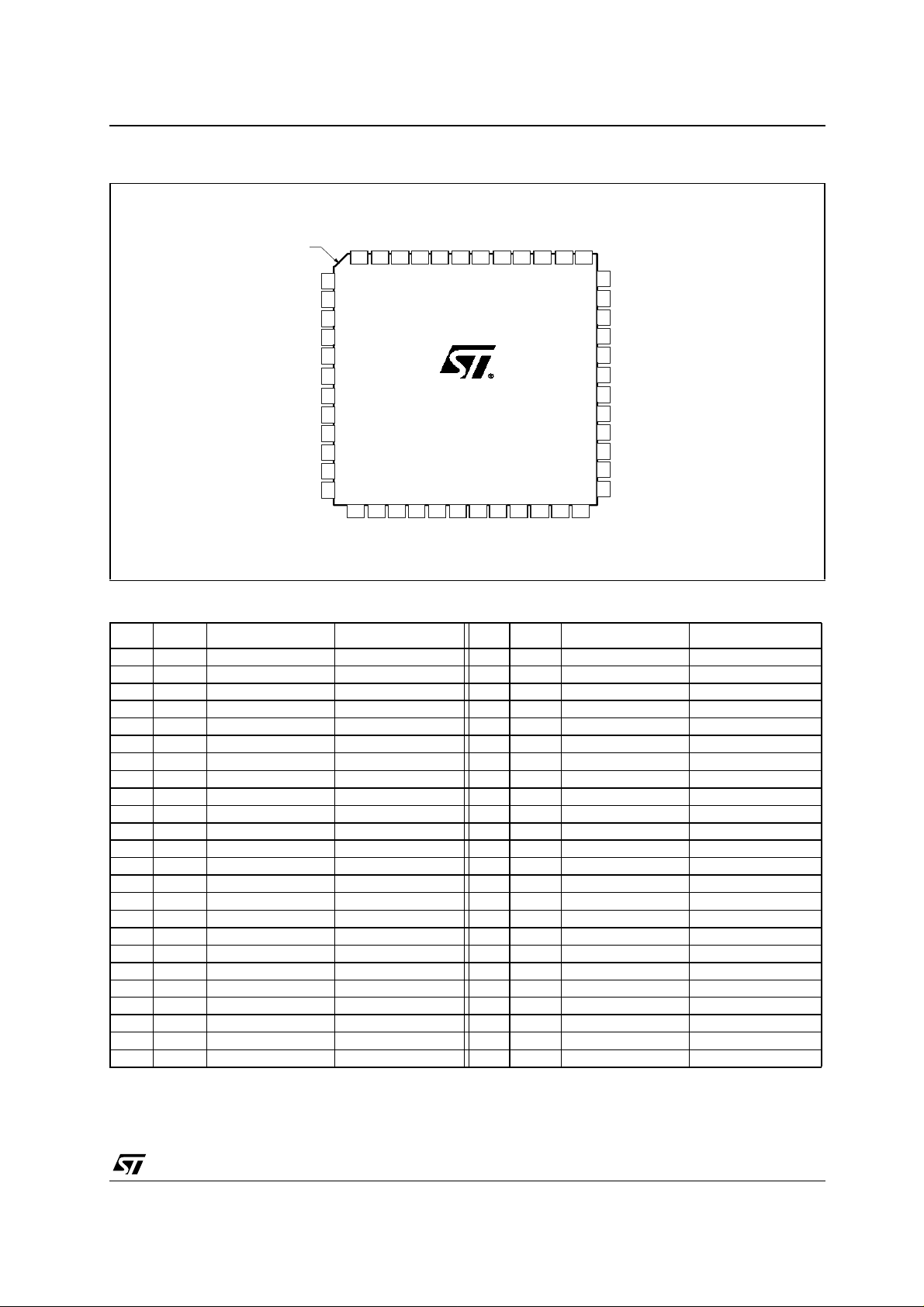
PIN CONNECTIONS (top view)
GNDBE
VCCBE
VCCBI
SRC
OEB
NC
GNDBE
GNDBI
DGND
VCCBENCOR
DR
23 24
NC
37
NC
36
D0 (LSB)
35
D1
34
33
D2
32
D3
31
D4
30
D5
D6
29
D7
28
D8
27
26
D9
25
D10
D11 (MSB)
index
corner
IPOL
VREFP
VREFM
AGND
VIN
AGND
VINB
AGND
INCM
AGND
AVCC
AVCC
AVCC
AGND
AVCC
DFSB
48 44 43 42 41 40 39 38
46 45
47
1
2
3
4
5
6
7
8
9
10
11
12
13 14 15 16 17 18 19 20 21 22
DVCC
DVCC
TSA1201
CLK
DGND
DGND
PACKAGE
7 x 7 mm TQFP48
APPLICATIONS
■ High speed data acquisition
■ Medical imaging and ultrasound
■ Portable instrumentation
■ High speed DSP interface
■ Digital communica t ion - IF s ampling
March 2001
1/20
Page 2

TSA1201
ABSOLUTE MAXIMUM RATINGS
Symbol Parameter Values Unit
AVCC
DVCC
VCCBI
VCCBE
Analog Supply voltage
Digital Supply voltage
Digital buffer Supply voltage
Digital buffer Supply voltage
Tstg Storage temperature +150 °C
Electrical Static Discharge
ESD
- HBM
- CDM-JEDEC Standard
1. All voltages v al ues, except diffe rential vol tage, are with respect to net work ground termi nal. The m agnitude of input and outpu t volt ag es
must neve r exceed -0. 3V or VCC+0V
OPERATING CONDITIONS
Symbol Parameter Test conditions Min Typ Max Unit
AVCC Analog Supply voltage 2.25 2.5 2.7 V
DVCC Digital Supply voltage 2.25 2.5 2.7 V
VCCBI Internal (quiet) buffer Supply voltage 2.25 2.5 2.7 V
VCCBE External (noisy) buffer Supply voltage 2.25 2.5 3.5 V
VREFP Forced top voltage reference 0.8 - AVCC V
VREFM Bottom internal reference voltage input 0 1 V
1)
1)
1)
1)
0 to 3.3 V
0 to 3.3 V
0 to 3.3 V
0 to 3.6 V
2
KV
1.5
BLOCK DIAGRAM
VIN
IN CM
VINB
CLK
+2.5V
Timing
+2.5V/3.3V
stage stage
1
GND
2
Sequ en cer-pha se sh ifting
Dig ita l d a ta cor re ctio n
stage
n
Buffers
VREFP
Reference
circuit
GNDA
IPOL
VREFM
DFSB
SRC
OEB
DR
DO
TO
D11
OR
2/20
Page 3
PIN CONNECTIONS (top view)
index
corner
1
IPOL
2
VREFP
AGND
VIN
AGND
VINB
AGND
INCM
AGND
AVCC
AVCC
3
4
5
6
7
8
9
10
11
12
VREFM
GNDBE
VCCBE
AVCC
AGND
AVCC
DFSB
OEB
47
48 44 43 42 41 40 39 38
46 45
VCCBI
SRC
NC
TSA1201
13 14 15 16 17 18 19 20 21 22
DVCC
DVCC
DGND
CLK
DGND
DGND
GNDBE
GNDBI
VCCBENCOR
DR
23 24
NC
37
D11 (MSB)
36
35
34
33
32
31
30
29
28
27
26
25
TSA1201
NC
D0 (LSB)
D1
D2
D3
D4
D5
D6
D7
D8
D9
D10
PIN DESCRIPTION
Pin No Name Description Observation Pin No Name Description Observation
1 IPOL Analog bi as current input 25 D10 Digital outp ut CMOS output (2.5V/3.3V)
2 VREFP To p voltage re ference 1V 26 D9 Digital outp ut CMOS output (2.5V/3.3V)
3 VREFM Bottom voltage refer ence 0V 27 D8 Digital output CMOS output (2.5V/3.3V)
4 AGND Analog ground 0V 28 D7 Digital output CMOS output (2.5V/3.3V)
5 VIN Analog input 1Vpp 29 D6 Digital output CMOS output (2.5V/3.3V)
6 AGND Analog ground 0V 30 D5 Digital output CMOS output (2.5V/3.3V)
7 VINB Inverted analog input 1Vpp 31 D4 Digital output CMOS output (2.5V/3.3V)
8 AGND Analog ground 0V 32 D3 Digital output CMOS output (2.5V/3.3V)
9 INCM Input common mode 0.5V 33 D2 Digital output CMOS output (2.5V/3.3V)
10 AGND Analog ground 0V 34 D1 Digital output CMOS output (2.5V/3.3V)
11 AVCC Analog power supply 2.5V 35 D0(LSB) Least Significant Bit output CMOS output (2.5V/3.3V)
12 AVCC Analog power supply 2.5V 36 NC Non connected
13 DVCC Digital power supply 2.5V 37 NC Non con nected
14 DVCC Digital power supply 2.5V 38 DR Data Ready output CMOS output (2.5V/3.3V)
15 DGND Digital ground 0V 39 VCCBE Digital Buffer po wer su pply 2.5V/3.3V
16 CLK Clock input 2.5V compatible CMOS input 40 GND BE Digital Buffer ground 0V
17 DGND Digital ground 0V 41 VCCBI Digital Buff er power supply 2.5V
18 NC Non connec ted 42 NC Non connected
19 DGND Digita l ground 0V 43 SRC Slew ra te cont r ol input 2.5V/3.3V CMOS input
20 GNDBI Digital buffer ground 0V 44 OEB Output Enable input 2.5V/3.3V CMOS input
21 GNDBE Digital buffer ground 0V 45 DFSB Data Format Select input 2.5V/3.3V CMOS input
22 VCCBE Digital buffer power supply 2.5V/3.3V 46 AVCC Analog power supply 2.5V
23 OR Out Of Range output CMOS output (2.5V/3.3V) 47 AVCC Analog power supply 2.5V
24 D11(MSB) Most Significant Bit output CMOS output (2.5V/3.3V) 48 AGND Analog ground 0V
3/20
Page 4

TSA1201
ELECTRICAL CHARACTERISTICS
AVCC = DVCC = VCCBE = VCCBI = 2.5V,Fs= 50Msps,Fin=2MHz, Vin@ -1dBFS, VREFM=0V
Tamb = 25°C (unless otherwise specified)
TIMING CHARACTERISTICS
Symbol Parameter Test conditions Min Typ Max Unit
FS Sampling Frequency 0.5 50 MHz
DC Clock Duty Cycle 45 50 55 %
TC1 Clock pulse width (high) 9 10 ns
TC2 Clock pulse width (low) 9 10 ns
Tod
Data Output Delay (Fall of Clock
to Data Valid)
Tpd Data Pipeline delay 5.5 cycles
Ton
Toff
Falling edge of OEB to digital
output valid data
Rising edge of OEB to digital
output tri-state
6pF load capacitance
8ns
1ns
1ns
TIMING DIAGRAM
N-3
CLK
OEB
Tod
DATA
OUT
DR
N-2
N-1
N+2
N+1
N
Tpd + Tod
Toff
N+3
N-3
N+4
N+5
N+6
Ton
N-1N-4N-5N-6N-7N-8N-9
N
4/20
HZ state
Page 5

TSA1201
CONDITIONS
AVCC = DVCC = VCCBE = VCCBI = 2.5V,Fs= 50Msps,Fin=2M Hz, Vin@ -1dBFS, VRE FM=0V
Tamb = 25°C (unless otherwise specified)
ANALOG INPUTS
Symbol Parameter Test conditions Min Typ Max Unit
VIN-VINB Full scale reference voltage 2.0 Vpp
Cin Input capacitance 7.0 pF
Rin Differential input resistance 5 MΩ
BW Analog Input Bandwitdh Vin@Full Scale, Fs=50Msps 1000 MHz
ERB
1. See parameters definiti on for more in formation .
Effective Resolution Bandwidth
REFERENCE VOLTAGE
Symbol Parameter Test conditions Min Typ Max Unit
1)
90 MHz
VREFP Top internal reference voltage
Tmin= -40°C to Tmax= 85°C
Vpol Analog bias voltage
Tmin= -40°C to Tmax= 85°C
VINCM Input common mode voltage
Tmin= -40°C to Tmax= 85°C
1. Not f ul l y tested over the temperat ure range. Guaranted by sampling.
0.79 1.0 1.16 V
1)
0.79 1.16 V
1.08 1.15 1.22 V
1)
1.07 1.23 V
0.40 0.55 0.65 V
1)
0.4 0.65 V
5/20
Page 6

TSA1201
CONDITIONS
AVCC = DVCC = VCCBE = VCCBI = 2.5V,Fs= 50Msps,Fin=2M Hz, Vin@ -1dBFS, VRE FP=1V,
VREFM=0V
Tamb = 25°C (unless otherwise specified)
POWER CONSUMPTION
Symbol Parameter Test conditions Min Typ Max Unit
Power consumption in normal
Pd
operation mode
1)
Tmin= -40°C to Tmax= 85°C
1)
ICCA Analog Supply current
Tmin= -40°C to Tmax= 85°C
1)
ICCD Digital Supply Current
Tmin= -40°C to Tmax= 85°C
1)
ICCBI Digital Buffer Supply Current
Tmin= -40°C to Tmax= 85°C
1)
ICCBE Digital Buffer Supply Current
Tmin= -40°C to Tmax= 85°C
ICCBEZ
Rthja
1. Equivalent lo ad: Rl oad= 470 Ω and Cload= 6pF
2. Not f ul l y tested over the temperat ure range. Guaranted by sampling.
Digital Buffer Supply Current in
High Impedance Mode
Junction-ambient ther ma l resistance (TQFP48)
2)
2)
2)
2)
2)
150 158 mW
165 mW
46 51 mA
55 mA
1.9 2.2 mA
2.2 mA
0.3 0.4 mA
0.4 mA
9.8 10.8 mA
10.8 mA
45mA
80 °C/W
DIGITAL INPUTS AND OUTPUTS
Symbol Parameter Test conditions Min Typ Max Unit
Clock input
VIL Logic "0" voltage 0 0.8 V
VIH Logic "1" voltage 2.0 2.5 V
Digital inputs
VIL Logic "0" voltage 0
VIH Logic "1" voltage
0.75 x
VCCBE
VCCBE V
0.25 x
VCCBE
Digital Outputs
VOL
VOH
Logic "0" voltage
Logic "1" voltage
Iol=10µA
Ioh=10µA 0.9 x
VCCBE
0.1 x
0
VCCBE
VCCBE V
IOZ High Impedance leakage current OEB set to VIH -2.5 2.5 µA
C
Output Load Capacitance 15 pF
L
6/20
V
V
Page 7

TSA1201
CONDITIONS
AVCC = DVCC = VCCBE = VCCBI = 2.5V,Fs= 50Msps, Vin @ -1d BFS , VR EFP =1V, VREFM=0V
Tamb = 25°C (unless otherwise specified)
ACCURACY
Symbol Parameter Test conditions Min Typ Max Unit
OE Offset Error
DNL Differential Non Linearity
INL Integral Non Linearity
Monotonicity and no missing
codes
Fin= 2MHz, VIN@+1dBFS 2.45 mV
Fin= 2MHz, VIN@+1dBFS ±0.6 LSB
Fin= 2MHz, VIN@+1dBFS ±1.7 LSB
Guaranted
DYNAMIC CHARACTERISTICS
Symbol Parameter Test conditions Min Typ Max Unit
SFDR Spurious Free Dynamic Range
Fin= 15MHz
Fin= 15MHz
SNR Signal to Noise Ratio
Fin= 15MHz
Fin= 15MHz
Fin= 15MHz
THD Total Harmonics Distorsion
Fin= 15MHz
SINAD
Signal to Noise and DistorsionRatio
Fin= 15MHz
Fin= 15MHz
Fin= 15MHz
ENOB Effective Number of Bits
Fin= 15MHz
1. Equivalent lo ad: Rl oad= 470 Ω and Cload= 6pF
2.
Tmin= -40°C to Tmax= 85°C. Not fully test ed over the tem perature range. Guara nted by sampli ng.
1)
2)
1)
2)
1)
2)
1)
2)
1)
2)
61.6 64.9 dB
60.7 dB
61 64.4 dB
60 dB
10 10.5 bits
9.9 bits
-77.2 -68 dBc
-67 dBc
-74.3 -68 dB
-64 dB
7/20
Page 8

TSA1201
DEFINITIONS OF SPECIFIED PARAMETERS
STATIC PARAMETERS
Static measurements are performed through
method of histograms on a 2MHz input signal,
sampled at 50Msps, which is high e nough to fully
characterize the test frequency response. The
input level is +1dBFS to saturate the signal.
Differen tial N on Li n e ari ty (DNL)
The average de viation of any output code width
from the ideal code width of 1LSB.
Integral Non linearity (INL)
An ideal c onverter pres ents a t ransf er f unct ion as
being the straight line from the starting code to the
ending code. The INL is the deviation for each
transition from this ideal curve.
DYNAMIC PARAMETERS
Dynamic measurements are performed by
spectral analysis, appl ied to an i nput sinew ave of
various frequencies and sampled at 50Msps.
Spurious Free Dynamic Range (SFDR)
The ratio between the power of the worst spurious
signal (not always an harmonic) and the amplitude
of fundamental tone (signal power) over the full
Nyquist band. It is expressed in dBc.
Total Harmonic Distortion (THD)
The ratio of the rm s sum of the first five harmo nic
distortion components to the rms value of the
fundamental line. It is expressed in dB.
Signal to Noise Ratio (SNR)
The ratio of the rms value of the fundamental
component to the rms sum of all other spectral
components in the Nyquist band (f
/2) excluding
s
DC, fundamental and the first five harmonics.
SNR is reported in dB.
Signal to Noise and Distorsion Ratio (SINAD)
Similar ratio as for SNR but including the harmonic
distortion components in the noise figure (not DC
signal). It is expressed in dB.
From the SINAD, the Effective Number of Bits
(ENOB) can easily be deduced using the formula:
SINAD= 6.02 × ENOB + 1.76 dB.
When the applied signal is not Full Scale (FS), but
has an A
amplitude, the SINAD expression
0
becomes:
SINAD= 6.02 × ENOB + 1.76 dB + 20 log (2A
/FS)
0
The ENOB is expressed in bits.
Analog Input Bandwidth
The maximum analog input frequency at which the
spectral response of a full power signal is reduced
by 3dB. Higher values can be achieved with
smaller input levels.
Effective Resolution Bandwidth (ERB)
The band of input signal frequencies that the ADC
is intended to convert without loosin g linearity i.e.
the maximum analog input frequency at which the
SINAD is decreased by 3dB or t he ENOB b y 1/2
bit.
Pipeline delay
Delay between the initial sample of the analog
input and the availability of the corresponding
digital data output,on the output bus. Also called
data latency. It is expressed as a num ber of clock
cycles.
8/20
Page 9

Static parameter: Integral Non Linearity
Fs=50MSPS; Fin=1MHz; Icca=45mA; N=131072pts
3
2
1
0
INL (LSBs)
-1
-2
-3
0 5 00 1000 1500 2000 2500 3000 3500 4000
Static parameter: Differential Non Linearity
Fs=50MSPS; Fin=1MHz; Icca=45mA; N=131072pts
2
1.5
1
0.5
0
DNL (LSBs)
-0.5
-1
-1.5
-2
0 500 1000 1500 2000 2500 3000 3500 4000
TSA1201
Output Code
Output C ode
Linearity vs. VCCA
Fs=50MSPS; Icca=45mA; Fin=10MHz
67
66.5
66
65.5
65
64.5
(dB)
64
63.5
63
Dynamic parameters
62.5
62
2.25 2.35 2.45 2.55 2.65
SNR
SINAD
ENOB
VCCA (V )
12
11.8
11.6
11.4
11.2
11
10.8
10.6
10.4
10.2
10
Distortion vs. VCCA
Fs=50MSP S; Icca=45 mA ; Fin=10 MHz
-72
-73
-74
-75
-76
-77
-78
Dynamic Parameters (dB)
-79
-80
-81
-82
SFDR
2.25 2.35 2.45 2.55 2.65
VCCA (V)
ENOB (bits)
THD
9/20
Page 10

TSA1201
)
)
Linearity vs. VCCD
Fs=50MSP S; Icca=45m A ; Fin=10 MHz
66
65.5
65
64.5
64
63.5
(dB)
63
62.5
62
Dynamic parameters
61.5
61
2.25 2.35 2.45 2.55 2.65
SNR
SINAD
ENOB
VCCD (V )
Linearity vs. VCCBE
Fs=50MSP S; Icca=45m A ; Fin=10 MHz
66
65
64
63
(dB)
62
61
Dynamic parameters
60
2.25 2.35 2.45 2.55 2.65
SNR
SINAD
ENOB
VCCBE ( V)
12
11.8
11.6
11.4
11.2
11
10.8
10.6
10.4
10.2
10
12
11.8
11.6
11.4
11.2
11
10.8
10.6
10.4
10.2
10
Distortion vs. VCCD
Fs=50MSP S; Icca=45 mA ; Fin=10 MHz
-71
-73
-75
-77
-79
ENOB (bits)
-81
-83
Dynamic parameters (dB)
-85
2.25 2.35 2.45 2.55 2.65
SFDR
VCCD (V)
Distortion vs. VCCBE
Fs=50MSPS; Icca=45mA; Fin=10MHz
-72
-73
-74
-75
-76
-77
-78
ENOB (bits)
-79
-80
-81
Dynamic Parameters (dB)
-82
2.25 2.35 2.45 2.55 2.65
THD
SFDR
VCCBE (V)
THD
Linearity vs. Fs
Icca=45mA; Fin=10 MHz
70
68
66
64
62
60
58
56
54
52
Dynamic parameters (dB
50
15 2 5 35 45 55 65 75
SNR
SINAD
ENOB
Fs (MHz)
12
11.5
11
10.5
10
9.5
Distortion vs. Fs
Icca=45mA; Fin=10 MHz
-50
-55
-60
-65
-70
ENOB (bits)
-75
-80
-85
Dynamic parameters (dB
-90
15 25 35 45 55 65 75
THD
SFDR
Fs (MHz)
10/20
Page 11

TSA1201
)
5
5
)
5
5
)
)
Linearity vs. Fin
Fs=50MHz; Icca=45mA
80
75
70
65
60
55
ENOB
SNR
SINAD
Dynamic parameters (dB
50
020406080
Fin (MHz)
Linearity vs.Temperatur e
Fs=49.7MSPS; Icca=45m A; Fin=15M Hz
69
67
65
63
61
59
57
Dynamic Parameters (dB
55
-40 10 60 110
SNR
SINAD
ENOB
Temperature (°C)
12
11.
11
10.
10
9.5
12
11.
11
10.
10
9.5
9
8.5
8
7.5
7
Distortion vs. Fin
Fs=50MHz; Icca=45mA
-60
-65
-70
-75
-80
-85
THD
SFDR
Dynamic parameters (dB
-90
0 20406080
Fin (MHz)
Distortion vs. Temperature
Fs=49.7MSPS; Icca=45m A; Fin=15M Hz
90
85
80
75
70
65
60
55
Dynamic Parameters (dB
50
-40 10 60 110
THD
SFDR
Temp e ratu r e (°C)
Single- tone 16K FF T at 50 Msps
Fin=94.5MHz; Icca=45mA, Vin@-0.5dBFS
0
-20
-40
-60
-80
-100
-120
P o wer Spectru m (dB )
-140
Frequency (MHz)
151050
20
11/20
Page 12

TSA1201 APPLICATION NOTE
DETAILED INFORMATION
The TSA1201 is a High Speed analog to digital
converter based on a pipeline architecture and the
latest deep submicron CMOS process to achieve
the best performances in terms of linearity and
power consumption.
The pipeline structure consists of 11 internal
conversion stages in which the analog signal is
fed and sequencially converted into digital data.
Each 10 first stages consists of an Analog to
Digital converter, a Digital to Analog converter, a
Sample and Hold and a gain of 2 amplifier. A
1.5-bit conversion resolution is achieved in each
stage. The latest stage simply is a comparator.
Each resulting LSB-MSB couple is then time
shifted to recover from the delay caused by
conversion. Digital data correction completes the
processing by recov ering from the redunda ncy of
the (LSB-MSB) couple for each stage. The
OPERATIONAL MODES DESCRIPTION
Inputs Outputs
Analog input differential level DFSB OEB SRC OR D R Most Significant Bit (MSB)
(VIN-VINB) > RANGE H L X H CLK D11
-RANGE > (VIN-VINB) H L X H CLK D11
RANGE> (VIN-VINB) >-RANGE H L X L CLK D11
(VIN-VINB) > RANGE L L X H CLK D11 Complemented
-RANGE > (VIN-VINB) L L X H CLK D11 Complemented
RANGE> (VIN-VINB) >-RANGE L L X L CLK D11 Complemented
X X H X HZ HZ HZ
X X X H X CLK 25Msps compliant slew rate
X X X L X CLK 50Msps compliant slew rate
corrected data are outputed through the digital
buffers.
Signal input is sampled on the rising edge of the
clock while digital outputs are delivered on the
falling edge of the clock.
The advantages of such a convert er reside in the
combination of pipeline architec ture and the most
advanced technologies. The highest dynamic
performances are achieved while consumption
remains at the lowest level.
Some functionalites have been added in order to
simplify as much as possible the application
board. These operational m odes are described in
the following table.
The TSA1201 is pin to pin compatible with the
8bits/40Msps TSA0801, the 10bits/25Msps
TSA1001 and t he 10bits/50Msps TSA1002. T his
ensures a conformity with the product family and
above all, an easy upgrade of the application
Data Format Select (DFSB)
When set to low level (VIL), the digital input DFSB
provides a tw o’s complement d igital output MSB.
This can be of interest when performing some
further signal processing.
When set to high level (VIH), DFSB provides a
standard binary output coding.
12/20
Output Enable (OEB)
When set to low level (VIL), all digital outputs
remain active and are in low impedance state.
When set to high level (VIH), all digital outputs
buffers are in high impedance state while the
converter goes on sampling. When OEB is set to a
low level again, t he data are then present on the
output with a very short Ton delay.
Therefore, this allows the chip select of the device.
The timing diagram summarizes this functionality.
Page 13

TSA1201
Slew Rate Control (SRC)
When set to high level (VIH), all digital outputs
currents are limited to a clamp value so that digital
noise power is reduced to its min imum. Rise and
fall times just match 25MHz sampling rate
assuming the load capacitance on each digital
output remains below 10pF.
When set to low level (VIL), the maximum digital
output current increases so that rise and fall times
just match the 50MHz sampling rate assuming the
load capacitance o n each digital output remains
below 10pF.
Out of Range (OR)
This function is im plemented on the output stage
in order to set up an "Out of Range" flag whenever
the digital data is over the full scale range.
Typically, there is a detection of all the dat a bei ng
at ’0’ or all the data being at ’1’. This ends up with
an output signal OR which is in low level state
(VOL) when the data stay within in the range, or in
high level state (VOH) when the data are out of the
range.
Data Ready (DR)
The Data Ready output is an image of the clock
being synchronized on the output data (D0 to
D11). This is a very helpful signal that simplifes
the synchronization of the measurement
equipment or the controling DSP.
As digital output, DR goes into high impedance
state when OEB is asserted to high level as
described in the timing diagram.
DRIVING THE ANALOG INPUT
Differentia l inp u t s
The TSA1201 has been designed to obtain
optimum performances when being differentially
driven. An RF transformer is a good way to
achieve such performances.
Figure 1 describes the schematics. The input
signal is fed to the primary of the transformer,
while the secondary drives both ADC inputs. The
common mode voltage of the ADC (INCM) is
connected to the center-tap of the secondary of
the transformer in order to bias the input signal
around this common voltage, internally set to
0.56V. It determines the DC component of the
analog signal. As being an high impedance inp ut,
it acts as an I /O and can be externally driven to
adjust this DC component. The INCM is
decoupled to maintain a low noise level on this
node. Our evaluat ion board i s m ount ed with a 1: 1
ADT1-1 transformer from Minicircuits. You might
also use a higher impedance ratio (1:2 or 1:4) to
reduce the driving requirement on the analog
signal source.
Each analog input can drive a 1Vpp amplitude
input signal, so the resultant differential amplitude
is 2Vpp.
Figure 1 : Differential input configuration
Analog source
50Ω
ADT1-1
1:1
330pF
100pF
10nF
VIN
TSA1201
VINB
INCM
470nF
Single-ended input configuration
Some applications may require a single-ended
input. This is easily achieved with the
configuration reported on Figure 2 for an
AC-coupled input or on Figure 3 and 4 for a
DC-coupled input..
In the case of AC-coupled analog input, it is
recommended to connect the other analog input to
the common mode voltage of the circuit (INCM) so
as to properly bias the ADC. The INCM may
remain at the same internal level (0.56V) thus
driving only a 1Vpp input ampl itude, or it mus t be
increased to 1V to drive a 2Vpp input amplitude.
Figure 2 : AC-coupled Single-ended input
Signal so urce
50Ω
100nF
330pF
VIN
TSA1201
VINB
INCM
10nF
470nF
1V
In the case of DC-coupled analo g input, Figure 3
shows the configuration for a 2Vpp input signal.
The DC component is driven by V REFP which is
connected to INCM and VINB and therefore
imposes its voltage. VREFM being connected to
ground, a dynamic of 2Vpp is achievable.
Figure 4 describes the configuration for a 1Vpp
analog signal. In this case, VREFM is connect ed
13/20
Page 14

TSA1201
to VINB and INCM. The latest imposes its voltage.
VREFP being internal ly set to 1V, the dynamic is
then 1Vpp.
Figure 3 : DC-coupled 2Vpp analog input
Analog
DC
Analog+DC
330pF
VIN
TSA1201
VINB
INCM
10nF
VREFP
VREFM
470nF
Figure 4 : DC-coupled 1Vpp analog input
Analog
DC
Analog+DC
VIN
TSA1201
VINB
INCM
VREFM
REFERENCE CONNECTION
Inte rnal re f erence
In the standard configuration, the ADC is bi ased
with the internal reference voltage. VREFM pin is
connected to Analog Ground while VREFP is
internally set to a voltage of 1.0V. It is
recommended to d ecouple the V RE F P in order t o
minimize low and high frequency noise. Refer to
Figure 5 for the schematics.
Figure 5 : Internal reference setting
VIN
1.0V
VREFP
330pF
10nF
470nF
TSA1201
VINB
VREFM
External re fere nce
330pF
10nF
470nF
IF-sampling
Software radio has become a common mode for
receiving data through RF receivers. Its main
advantage being to di gitally implement what was
originally done with analog functions such as
discriminators, demodulation and filtering.
Originally, bipolar process was mainly used
because they provided high transistor transit
frequency, while pure CMOS technol ogy showed
a lower one. With new CMOS process and c ircuit
topology, higher frequencies are now achieved.
The TSA1201 has been specifically designed to
meet the requirement of sampling at Intermediate
Frequency. For this purpose, the Track-and-Hold
of the first pipeline s tage has been b uilt to ensure
the global linearity of the overall ADC to p erform
the right characteristics.
Our proprietary Track-and-Hold has a patented
switch control system to enable the pe rformances
not to be degraded as input signal frequency
increases.
As a result, an analog bandwidth of 1GHz is
achieved.
It is possible to use an external reference vo ltage
instead of the internal one for specific applications
requiring even better linearity or enhanced
temperature behaviour. In this case, the amplitude
of the external voltage mu st be at least equal to
the internal one (1.0V). Using the
STMicroelectronics Vref TS8 21 leads to optimum
performances when configured as shown on
Figure 6.
Figure 6 : External reference setting
1k
Ω
10nF
470nF
VCCA
VIN
TSA 1201
VINB
VREFP
VREFM
330pF
TS821
external
reference
This can be very helpful for example for
multichannel application to kee p a good matching
over the sampling frequency range.
14/20
Page 15

Clock input
The quality of your converter is very dependant on
your clock input accuracy, in terms of aperture
jitter; the use of low jitter crystal controlled
oscillator is recommended.
The duty cycle must be between 45% and 55%.
The clock power supplies must be separated from
the ADC output ones to avoid digital noise
modulation at the output.
It is recommended to always keep the circuit
clocked, even at the lowest specified sampling
frequency of 0.5Msps, bef ore applying the supply
voltages.
Power co nsumption op tim i za tio n
The internal architecture of the TSA1 201 enables
to optimize the power consumption according to
the sampling frequency of. For this purpose, a
resistor is placed between IPOL and the analog
Ground pins. Therefore, the total dissipation is
adjustable from 0.5Msps up to 50Msps. This
feature is of highest importance when power
saving conditions the application.
The TSA1201 will com bine highest pe rformances
and lowest consumption at 50Msps when Rpol is
equal to 12kΩ.
At lower sampling frequency range, this value of
resistor may be adjusted in order to decrease the
analog current without any degradation of
dynamic performances.
As an example, 40mW total power consumption is
achieved at 5 Msps with Rpol equal to 190kΩ and
35mW is dissipated at 1Msps with Rpol equal to
350kΩ.
The table below sums up the relevant data.
Figure 7 describes the behaviour of the converter
as sampling frequency increases and shows the
optimum in terms of analog current and
polarization resistor.
Total power consumption optimization
dependi ng on Rpol value
Fs (Msps) 5 35 50
Rpol (
kΩ)
Optimized
power (mW)
190 29 12
40 100 150
TSA1201
Figure 7 : Optimized power consumption
Fin=1MHz
200
180
160
140
120
100
80
Rpol(kOhms)
60
40
20
0
5 25456585
ICCA
RPOL
Fs(MHz)
Layout precautions
To use the ADC circuits in the best manner at high
frequencies, some precautions have to be taken
for power supplies:
- First of all, the implementation of 4 separate
proper supplies and ground planes (analog,
digital, internal and external buffer ones) on the
PCB is mandatory for high speed circuit
applications to provide low inductance and low
resistance common return.
The separation of the analog signal from the
digital part is essential to prevent noise from
coupling onto the input signal.
- Power supply bypass capacitors must be placed
as close as possible to the IC pins in order to
improve high frequency bypassing and reduce
harmonic distortion.
- Proper termination of all inputs and outputs must
be incorporated with output termination resistors;
then the amplifier load wi ll be only resistive and
the stability of the amplifier will be improved. All
leads must be wide and as short as possible
especially for the analog input in order to decrease
parasitic capacitance and inductance.
- To keep the capacitive loading as low as
possible at digital outputs, short lead lengths of
routing are essential to minimize currents when
the output changes. To minimize this output
capacitance, buffers or latches close to the output
pins will relax this constraint.
- Choose component sizes as small as possible
(SMD).
70
60
50
40
30
Icca(mA)
20
10
0
15/20
Page 16

TSA1201
EVAL1201 evaluation board
The characterization of the board has been made
with a fully ADC devoted test bench as shown on
Figure 8. The analog signal must be filtered to be
very pure.
The dataready signal is the acquisition clock of the
logic analyzer.
The ADC digital outputs are latched by the octal
buffers 74LCX573.
All characterization measurements have been
made with:
- SFSR=+0.5dB for static parameters.
- SFSR=-0.5dB for dynamic parameters.
Figure 8 : Analog to Digital Converter characterization bench
Power
HP8644B
Sine wave
Generator
Vin
HP8133A
ADC
evaluation
board
ck
Pulse
Generator
data
dataready
Logic
Analyzer
TLA704
HP8644B
Sine Wave
Generator
16/20
Page 17

Figure 9 : TSA1201 Evaluation board schematic
TSA1201
J6
J6
123456789
123456789
DR
DR
2
2
VCCB2
VCCB2
1
1
J17
VDDBUFF3V
J17
VDDBUFF3V
+
+
C34
47µ
C34
47µ
C37
C37
2
2
1
1
J13
J13
2
2
1
1
J11
J11
2
2
1
1
J10
OEB
J10
OEB
2
2
1
1
J9
DFSB
J9
DFSB
R10
47K
R11
47K
R10
47K
R11
47K
VCCB1
VCCB1
C28
C28
AVCC
AVCC
R12
47K
R13
47K
R12
47K
R13
47K
C16
C16
470nF
470nF
470nF
470nF
470nF
470nF
C26
C26
10nF
10nF
C39
C39
R19
R19
R18
R18
R17
R17
R16
R16
R15
R15
R14
R14
C25
C25
10nF
10nF
C27
C27
C14
C15
10nF
C14
C15
10nF
Raj1
47K
Raj1
47K
R2
1K
R2
1K
1011121314151617181920212223242526272829303132
1011121314151617181920212223242526272829303132
D1D2D3D4D5
D1D2D3D4D5
DO
DO
20
20
Q019Q118Q217Q316Q415Q514Q613Q7
Q019Q118Q217Q316Q415Q514Q613Q7
VCC
VCC
330pF
330pF
OEB1D02D13D24D35D46D57D68D79GND
OEB1D02D13D24D35D46D57D68D79GND
47K
47K
47K
47K
47K
47K
47K
47K
47K
47K
47K
47K
37
37
38
38
330pF
330pF
39
39
40
40
41
41
42
42
43
43
44
44
45
45
46
46
47
47
48
48
330pF
330pF
C11
C11
C12
C12
C13
C13
C31
C31
C32
C32
D6
D6
11
12
11
12
LE
LE
U2
U2
10
10
36
36
D0
D0
DR
DR
2.5VCCBUFF
2.5VCCBUFF
GNDBUFF
GNDBUFF
2.5VCCBUFF
2.5VCCBUFF
NC
NC
NC
NC
OEB
OEB
DFSB
DFSB
AVCC
AVCC
AVCC
AVCC
AGND
AGND
Ipol1VrefP2VrefM3AGND4Vin5AGND6VINB7AGND8INCM9AGND10AVCC11AVCC
Ipol1VrefP2VrefM3AGND4Vin5AGND6VINB7AGND8INCM9AGND10AVCC11AVCC
330pF
330pF
10nF
10nF
470nF
470nF
C30
330pF
C30
330pF
10nF
10nF
470nF
470nF
74LCX573
74LCX573
TSA1201
TSA1201
8-14bits ADC
TSA1002
8-14bits ADC
TSA1002
D7D8D9
D7D8D9
D10
D10
20
20
Q019Q118Q217Q316Q415Q514Q613Q7
Q019Q118Q217Q316Q415Q514Q613Q7
VCC
VCC
U3
U3
OEB1D02D13D24D35D46D57D68D79GND
OEB1D02D13D24D35D46D57D68D79GND
27
27
D928D829D730D631D532D433D334D235D1
D928D829D730D631D532D433D334D235D1
D1225D1126D10
D1225D1126D10
D13
D13
OR
OR
2.5VCCBUFF
2.5VCCBUFF
GNDBUFF
GNDBUFF
GNDBUFF
GNDBUFF
DGND
DGND
NC
NC
DGND
DGND
CLK
CLK
DGND
DGND
DVCC
DVCC
DVCC
DVCC
12
12
C2
330pF
C2
330pF
C4
10nF
C4
10nF
C3
470nF
C3
470nF
D11
D11
12
12
24
24
23
23
22
22
21
21
20
20
19
19
18
18
17
17
16
16
15
15
14
14
13
13
32PIN
32PIN
OR
OR
D12
D13
D12
D13
11
11
LE
LE
C38
C38
74LCX573
74LCX573
10
10
470nF
470nF
+
+
C29
C29
43
43
2
2
6
6
C33
C33
10nF
10nF
330pF
330pF
C40
C40
VCCB1
VCCB1
1
1
2
2
+
+
J18
VccB1
J18
C17
330pF
C18
10nF
C19
470nF
C17
330pF
C18
10µF
10µF
T1
T2-AT1-1WT
T1
T2-AT1-1WT
R3
R3
1
1
C20
330pF
C21
C20
330pF
C21
C24
10nF
C19
470nF
C24
50
50
10nF
C22
470nF
C23
10nF
C22
470nF
C23
VccB1
10µ
10µ
C35
47µ
C35
47µ
J4
CLJ/SMB
J4
CLJ/SMB
1
1
2
2
J16
CON2
J16
CON2
C36
47µ
C36
47µ
+
+
1
1
10µ
10µ
2
2
J15
DVCC
J15
DVCC
AVCC
AVCC
C5
330pF
C8
330pF
C5
330pF
C8
330pF
C1
100pF
C1
100pF
4326
4326
T2
T2
R1
50
R1
50
1
1
1
2
1
2
1
2
1
2
refP
refM
refP
refM
C6
10nF
C9
10nF
C6
10nF
C9
10nF
C7
470nF
C10
470nF
C7
470nF
C10
470nF
T2-AT1-1WT
T2-AT1-1WT
1
2
1
2
1
2
1
2
egl com mode
egl com mode
8
8
C41
10µF
C41
10µF
C42
47µF
C42
47µF
+
+
1
2
1
2
1
2
1
2
1
1
2
1
2
1
es com Mode
es com Mode
VCC
VCC
12
19
12
19
2
0
1
0
GND
GND
1
GND
GND
2
1
2
1
2
2
2
ndB2
ndB1
ndB2
ndB1
17/20
Page 18

TSA1201
Figure 10 : Printed circuit of evaluation board.
Print ed circuit boa rd - List of compon ents
Part Design Footprint Part Design Footprint Part Design Footprint P art Design Footprint
Part Design Footprint Part Design Footprint Part Design Footprint P art Design Footprint
ator
ator
Type
Type
10 uF C 2 4 1210
10 uF C 2 4 1210
10 uF C 2 3 1210
10 uF C 2 3 1210
10 uF C 4 1 1210
10 uF C 4 1 1210
10 uF C 2 9 1210
10 uF C 2 9 1210
100pF C1 603
100pF C1 603
10nF C12 603
10nF C12 603
10nF C39 603
10nF C39 603
10nF C15 603
10nF C15 603
10nF C40 603
10nF C40 603
10nF C27 603
10nF C27 603
10nF C4 603
10nF C4 603
10nF C21 603
10nF C21 603
10nF C31 603
10nF C31 603
10nF C6 603
10nF C6 603
10nF C9 603
10nF C9 603
10nF C18 603
10nF C18 603
1KΩR2 603
1KΩR2 603
32P IN J6 IDC32
32P IN J6 IDC32
330pF C25 603
330pF C25 603
330pF C26 603
330pF C26 603
18/20
ator
ator
Type
Type
330pF C33 603 470nF C7 805 AVCC J12 FICHE2MM
330pF C33 603 470nF C7 805 AVCC J12 FICHE2MM
330pF C20 603 470nF C16 805 CLJ/SMB J4 SMB/H
330pF C20 603 470nF C16 805 CLJ/SMB J4 SMB/H
330pF C8 603 470nF C19 805 AGND J19 FICHE2MM
330pF C8 603 470nF C19 805 AGND J19 FICHE2MM
330pF C2 603 470nF C3 805 DFSB J9 FICHE2MM
330pF C2 603 470nF C3 805 DFSB J9 FICHE2MM
330pF C5 603
330pF C5 603
330pF C11 603
330pF C11 603
330pF C30 603
330pF C30 603
330pF C17 603
330pF C17 603
330pF C14 603
330pF C14 603
47uF C36 C AP
47uF C36 C AP
47uF C34 C AP
47uF C34 C AP
47uF C35 C AP
47uF C35 C AP
47uF C42 C AP
47uF C42 C AP
470nF C22 805
470nF C22 805
470nF C32 805
470nF C32 805
470nF C37 805
470nF C37 805
470nF C38 805
470nF C38 805
470nF C13 805 74LCX573 U3 TSSOP 20 VrefP J2 FICHE2MM
470nF C13 805 74LCX573 U3 TSSOP 20 VrefP J2 FICHE2MM
470nF C28 805 74LCX573 U2 TSSOP 20 TSA1002 U1 TQFP48
470nF C28 805 74LCX573 U2 TSSOP 20 TSA1002 U1 TQFP48
470nF C10 805 CON2 J16 S IP2
470nF C10 805 CON2 J16 S IP2
Type
Type
47K
47K
47K
47K
47K
47K
47K
47K
47K
47K
47K
47K
47K
47K
47K
47K
47K
47K
47K
47K
47K
47K
50
50
50
50
ator
ator
Ω
Ω
R12 603 DGND J20 FICHE2MM
R12 603 DGND J20 FICHE2MM
Ω
Ω
R14 603 DVCC J15 FICHE2MM
R14 603 DVCC J15 FICHE2MM
Ω
Ω
R11 603 GndB 1 J22 FICHE2MM
R11 603 GndB 1 J22 FICHE2MM
Ω
Ω
Raj1 VR5 GndB2 J21 FICHE2MM
Raj1 VR5 GndB2 J21 FICHE2MM
Ω
Ω
R10 603 Mes c o m mo de J8 FICHE2MM
R10 603 Mes c o m mo de J8 FICHE2MM
Ω
Ω
R19 603 OEB J10 FICHE2MM
R19 603 OEB J10 FICHE2MM
Ω
Ω
R13 603 Regl com mode J7 FICHE2MM
R13 603 Regl com mode J7 FICHE2MM
Ω
Ω
R15 6 03 T2-AT1-1WT T2 AD T
R15 6 03 T2-AT1-1WT T2 AD T
Ω
Ω
R16 6 03 T2-AT1-1WT T1 AD T
R16 6 03 T2-AT1-1WT T1 AD T
Ω
Ω
R17 603 VccB1 J18 FICHE2MM
R17 603 VccB1 J18 FICHE2MM
Ω
Ω
R18 603 VDDBUFF3V J17 FICHE2MM
R18 603 VDDBUFF3V J17 FICHE2MM
Ω
Ω
R3 603 Vin J1 SMB/H
R3 603 Vin J1 SMB/H
Ω
Ω
R1 603 VrefM J5 FICHE2MM
R1 603 VrefM J5 FICHE2MM
Type
Type
TSA1201
TSA1201
ator
ator
Page 19

TSA1201
PACKAGE MECHANICAL DATA
48 PINS - PLASTIC PACKAGE
48 37
1
e
36
E3
E1
A
A2
A1
0,10 mm
.004 inch
SEATING PLANE
B
E
12
13 24
D3
25
c
D1
D
L1
L
0,25 mm
.010 inch
K
GAGE PLANE
Millimeters Inches
Dim.
Min. Typ. Max. Min. Typ. Max.
A 1.60 0.063
A1 0.05 0.15 0.002 0.006
A2 1.35 1.40 1.45 0.053 0.055 0.057
B 0.17 0.22 0.27 0.007 0.009 0.011
C 0.09 0.20 0.004 0.008
D 9.00 0.354
D1 7.00 0.276
D3 5.50 0.216
e 0.50 0.0197
E 9.00 0.354
E1 7.00 0.276
E3 5.50 0.216
L 0.45 0.60 0.75 0.018 0.024 0.030
L1 1.00 0.039
K 0° (min.), 7° (max.)
Information furnished is bel ieved to be accurate and reliable. However, STMicroe lectronics assumes no responsibility for the
consequences of use of such information nor for any infringement of patents or other rights of third parties which may result from
its use. No li cense is granted by i mp lication or otherwise under any patent or patent rights of STMicroelectronics. Specifications
mentioned in this publication ar e subject to change without notice. This publication supersedes and replaces all information
previously supplied. S TMicroelectronics products are not authorized for use as critica l components in life suppo rt devices or
systems without express written approval of STMicroelectronics.
Australi a - Brazil - Chi na - Finlan d - F rance - Germ any - Hong Kon g - I ndi a - Italy - Japan - Malay si a - Malta - Morocco
© The ST logo is a registered trademark of STMicroelectronics
© 2001 STM icroelectronics - P rinted in Fran ce - All Rig h ts Reserv ed
STMicroelectronics GROUP OF COMPANIES
Singapo re - Spain - Sweden - Swit zerland - Un i ted Kingdom
© http://www.st.com
19/20
Page 20

TSA1201
20/20
 Loading...