

Page 1
TSA0801
8-BIT, 40MSPS, 40mW A/D CONVERTER
■ 8-bit A/D converter in deep submicron
CMOS technology
■ Single supply voltage: 2.5V
■ Input range: 2Vpp differential
■ 40Msps sampling frequency
■ Ultra low power consumption: 40mW @
40MHz (10mW @ 5Msps)
■ ENOB=7.9 @ Nyquist
■ SFDR typically up to 67dB @ Fs=40Msps,
Fin=5MHz
■ Built-in reference voltage with external bias
capability
■ STMicroelectronics 8,10, 12 and 14-bits ADC
pinout compatibility
DESCRIPTION
The TSA0801 is an 8-bit, 40MHz sampling frequency Analog to Digital converter using a deep
submicron CMOS technology combining high performances and very low power consumption.
The TSA0801 is based on apipeline structure and
digital error correction to provide excellent static
linearity and go beyond 7.9 effective bits at
Fs=40Msps, and Fin=10MHz.
A voltage reference is integrated in the circuit to
simplify the design and minimize external components. It is nevertheless possible to usethe circuit
with an external reference.
Differential or single-ended analog inputs can be
applied to the converter. A tri-state capability is
available on the outputs. The output data can be
coded into two different formats. A Data Ready
signal is raised as the data is valid on the output
and can be used for synchronization purposes.
The TSA0801 is available in commercial (0 to
+70°C) and extended (-40 to +85°C) temperature
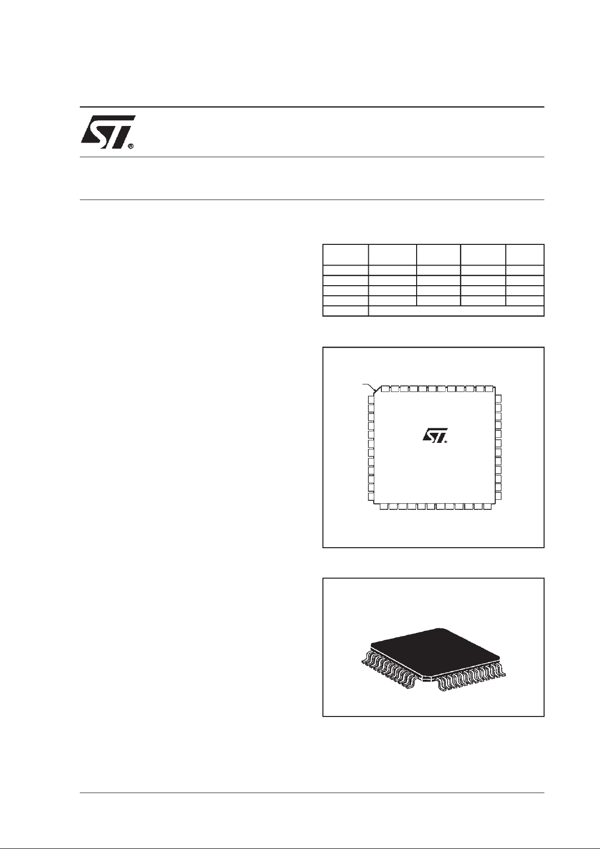
range, in a small 48 pins TQFPpackage.
ORDER CODE
Part Number
TSA0801CF 0°C to +70°C TQFP48 Tray SA0801C
TSA0801CFT 0°Cto +70°C TQFP48 Tape& Reel SA0801C
TSA0801IF -40°Cto +85°C TQFP48 Tray SA0801I
TSA0801IFT -40°C to +85°C TQFP48 Tape& Reel SA0801I
EVAL0801/AA Evaluation board
Temperature
Range
Package Conditioning Marking
PIN CONNECTIONS (top view)
AGND
index
corner
IPOL
VREFP
VREFM
AGND
VIN
AGND
VINB
AGND
INCM
AGND
AVCC
AVCC
AVCC
DFSB
48 44 43 42 41 40 39 38
46 45
47
1
2
3
4
5
6
7
8
9
10
11
12
13 14 15 16 17 18 19 2 0 21 22
DVCC
DVCC
DGND
TSA0801
CLK
OEB
DGND
VCCB
GNDB
NC
DGND
GNDB
GNDB
VCCB
23 24
VCCBNCOR
NC
DR
37
NC
36
NC
35
NC
34
33
NC
32
NC
31
D0(LSB)
30
D1
D2
29
D3
28
D4
27
26
D5
25
D6AVCC
D7 (MSB)
NC
PACKAGE
7 × 7 mm TQFP48
APPLICATIONS
■ Hand-held instrumentation
■ Camcorders
■ Computer scanners
■ Digital communication
October 2000
1/20
Page 2
TSA0801
ABSOLUTE MAXIMUM RATINGS
Symbol Parameter Values Unit
AVCC
DVCC
VCCB
Analog Supply voltage
Digital Supply voltage
Digital buffer Supply voltage
1)
1)
1)
IDout Digital output current -100 to 100 mA
Tstg Storage temperature +150 °C
Electrical Static Discharge:
ESD
- HBM
- CDM-JEDEC Standard
1) All voltages values, except differential voltage, are with respect to network ground terminal. The magnitude of input and output voltages
must never exceed -0.3V or VCC+0V
OPERATING CONDITIONS
Symbol Parameter Test conditions Min Typ Max Unit
AVCC Analog Supply voltage 2.25 2.5 2.7 V
DVCC Digital Supply voltage 2.25 2.5 2.7 V
VCCB Digital buffer Supply voltage 2.25 2.5 2.7 V
VREFP Forced top voltage reference 1.16 - AVCC V
VREFM Forced bottom reference voltage 0 0 0.5 V
0 to 3.3 V
0 to 3.3 V
0 to 3.3 V
2
KV
1.5
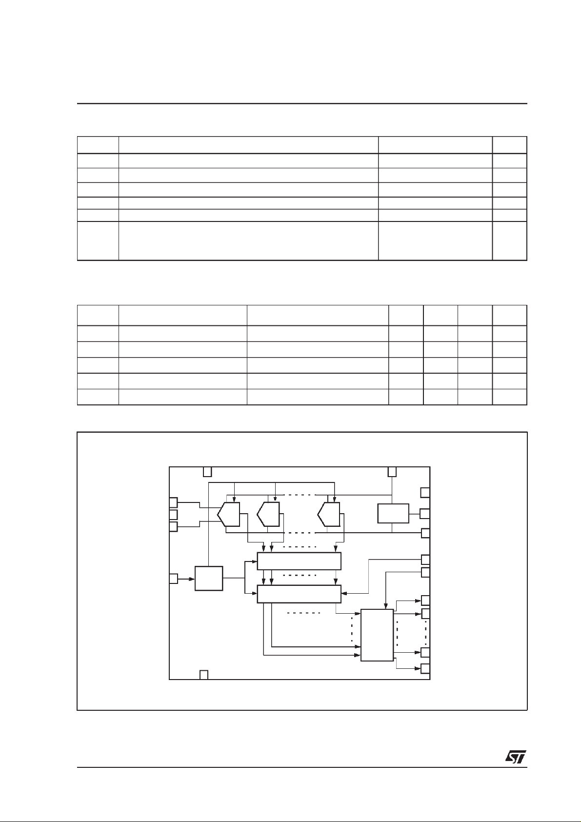
BLOCK DIAGRAM
INCM
VINB
CLK
VIN
+2.5V
stage stage stage
12 n
Sequencer-phase shifting
Timing
Digitaldata correction
GND
Buffers
VREFP
Reference
circuit
GNDA
IPOL
VREFM
DFSB
OEB
DR
DO
TO
D7
OR
2/20
Page 3
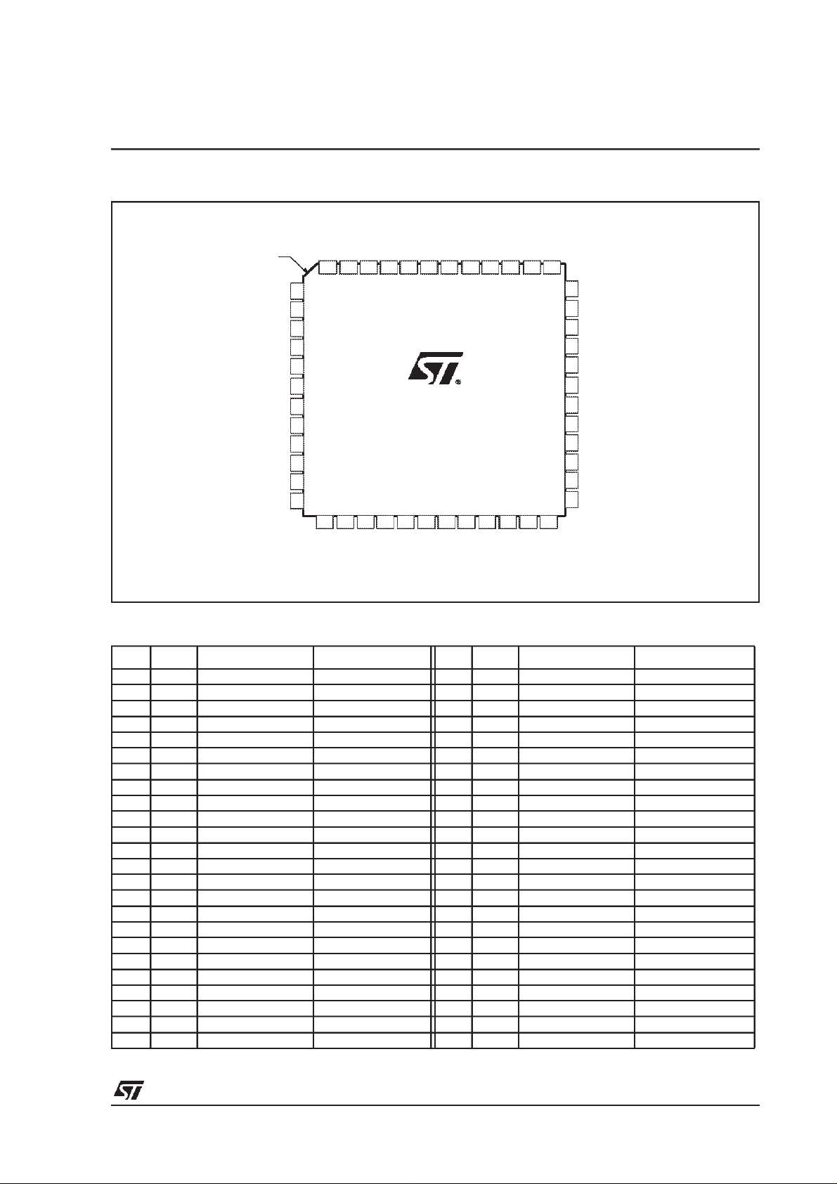
PIN CONNECTIONS (top view)
TSA0801
PIN DESCRIPTION
index
corner
IPOL
VREFP
VREFM
AGND
VIN
AGND
VINB
AGND
INCM
AGND
AVCC
AGND
AVCC
AVCC
DFSB
OEB
NC
NC
47
48 44 43 42 41 40 39 38
46 45
1
2
3
4
5
6
7
8
9
10
11
12
13 14 15 16 17 18 19 20 21 22
DVCC
DVCC
TSA0801
CLK
DGND
DGND
DGND
VCCB
GNDB
GNDB
GNDB
VCCB
DR
23 24
VCCBNCOR
NC
37
D7 (MSB)
36
35
34
33
32
31
30
29
28
27
26
25
NC
NC
NC
NC
NC
D0(LSB)
D1
D2
D3
D4
D5
D6AVCC
Pin No Name Description Observation Pin No Name Description Observation
1 IPOL Analog bias currentinput 25 D6 Digital output CMOS output (2.5V)
2 VREFP Top voltage reference 1V 26 D5 Digital output CMOS output (2.5V)
3 VREFM Bottom voltage referen ce 0V 27 D4 Digital output CMOS output (2.5V)
4 AGND Analog ground 0V 28 D3 Digital output CMOS output (2.5V)
5 VIN Analog input 1Vpp 29 D2 Digital output CMOS output (2.5V)
6 AGND Analog ground 0V 30 D1 Digital output CMOS output (2.5V)
7 VINB Inverted analog input 1Vpp 31 D0(LSB) Digital output CMOS output (2.5V)
8 AGND Analog ground 0V 32 NC Non conne cted
9 INCM Input common mode 0.5V 33 NC Non conne cted
10 AGND Analog ground 0V 34 NC Non connected
11 AVCC Analog power supply 2.5V 35 NC Non connected
12 AVCC Analog power supply 2.5V 36 NC Non conne cted
13 DVCC Digital power supply 2.5V 37 NC Non conne cted
14 DVCC Digital power supply 2.5V 38 DR Data Ready output CMOS output (2.5V)
15 DGND Digital ground 0V 39 VCCB Digital Buffer power supply 2.5V
16 CLK Clock input 2.5V compatibleCMOS input 40 GNDB Digital Buffer ground 0V
17 DGND Digital ground 0V 41 VCCB Digital Buffer power supply 2.5V
18 NC Non connected 42 NC Non conne cted
19 DGND Digital ground 0V 43 NC Non conne cted
20 GNDB Digital buffer ground 0V 44 OEB Output Enable input 2.5V compatibleCMOS input
21 GNDB Digital buffer ground 0V 45 DFSB Data Format Select input 2.5Vcompatib le CMOS input
22 VCCB Digital bufferpower supply 2.5V 46 AVCC Analog power supply 2.5V
23 OR Out Of Range output CMOS output(2.5V) 47 AVCC Analog power supply 2.5V
24 D7(MSB) Most SignificantBit output CMOS output(2.5V) 48 AGND Analog ground 0V
3/20
Page 4
TSA0801
ELECTRICAL CHARACTERISTICS
AVCC= DVCC = VCCB =2.5V,Fs= 40Msps,Fin=1MHz, Vin@ -1.0dBFS, VREFM = 0V
Tamb = 25°C (unless otherwise specified)
TIMING CHARACTERISTICS
Symbol Parameter Test conditions Min Typ Max Unit
FS Sampling Frequency 0.5 40 MHz
DC Clock Duty Cycle 45 50 55 %
TC1 Clock pulse width (high) 11 12.5 ns
TC2 Clock pulse width (low) 11 12.5 ns
Tod
Data Output Delay (Fall of Clock
to Data Valid)
Tpd Data Pipeline delay 6.5 cycles
Ton
Toff
Falling edge of OEB to digital
output valid data
Rising edge of OEB to digital
output tri-state
10pF load capacitance
5ns
1ns
1ns
TIMING DIAGRAM
N-1
CLK
OEB
Tod
DATA
OUT
DR
N-8
N+4
N+3
N+2
N-7
N+1
6.5 clk cycles
N-5N-6
N-4
N-3
N
Toff
N+5
N-2
N+6
N+7
N+8
Ton
N
N+1
HZstate
4/20
Page 5
TSA0801
CONDITIONS
AVCC = DVCC = VCCB = 2.5V, Fs= 40Msps,Fin= 1MHz, Vin@ -1.0dBFS, VREFM= 0V
Tamb = 25°C (unless otherwise specified)
ANALOG INPUTS
Symbol Parameter Test conditions Min Typ Max Unit
VIN-VINB Full scale reference voltage 2.0 Vpp
Cin Input capacitance 7.0 pF
BW Analog Input Bandwitdh Vin@-1dBFS, FS=40Msps 100 MHz
ERB
1) See parameters definition for more information
Effective Resolution Bandwidth
1)
REFERENCE VOLTAGE
Symbol Parameter Test conditions Min Typ Max Unit
60 MHz
VREFP Top internal reference voltage
Tmin= -40°C to Tmax= 85°C
Vpol Analog bias voltage
Tmin= -40°C to Tmax= 85°C
Ipol Analog bias current Normal operating mode 50 70 100 µA
Ipol Analog bias current Shutdown mode 0 µA
VINCM Input common mode voltage
Tmin= -40°C to Tmax= 85°C
1) Not fully tested over the temperature range. Guaranted by sampling.
1)
1)
1)
0.89 1.03 1.16 V
0.88 1.16 V
1.19 1.27 1.35 V
1.18 1.36 V
0.46 0.57 0.66 V
0.46 0.66 V
5/20
Page 6
TSA0801
CONDITIONS
AVCC = DVCC = VCCB = 2.5V, Fs=40Msps, Fin= 1MHz, Vin@ -1.0dBFS, VREFP=1V, VREFM= 0V
Tamb = 25°C (unless otherwise specified)
POWER CONSUMPTION
Symbol Parameter Test conditions Min Typ Max Unit
1)
ICCA Analog Supply current
Tmin= -40°C to Tmax= 85°C
1)
ICCD Digital Supply Current
Tmin= -40°C to Tmax= 85°C
1)
ICCB Digital Buffer Supply Current
Tmin= -40°C to Tmax= 85°C
ICCBZ
PdZ
Rthja
Rthjc
1) Rpol= 18K
2) Not fully tested over the temperature range. Guaranted by sampling.
Digital Buffer Supply Current in
High Impedance Mode
Power consumption in normal
Pd
operation mode
Power consumption in High
Impedance mode
Junction-ambient thermal resis-
tor (TQFP48)
Junction-case thermal resistor
(TQFP48)
Ω.
Equivalent load: Rload= 470Ω and Cload= 6pF
1)
1)
Tmin= -40°C to Tmax= 85°C
1)
DIGITALINPUTS AND OUTPUTS
15.8 20 mA
2)
21 mA
1.3 2 mA
2)
2mA
2.1 5 mA
2)
5mA
50 110 µA
48 60 mW
2)
62 mW
43 55 mW
80 °C/W
18 °C/W
Symbol Parameter Test conditions Min Typ Max Unit
Digital inputs
VIL Logic ”0” voltage 0.8 V
VIH Logic ”1” voltage 2.0 V
Digital Outputs
VOL Logic ”0” voltage Iol=10µA 0.4 V
VOH Logic ”1” voltage Ioh=10µA 2.4 V
IOZ High Impedance leakage current OEB set to VIH -1.5 1.5 µA
C
Output Load Capacitance 15 pF
L
ACCURACY
Symbol Parameter Test conditions Min Typ Max Unit
OE Offset Error mV
DNL Differential Non Linearity -0.5 +0.5 LSB
INL Integral Non Linearity -1 +1 LSB
Monotonicity and no missing
6/20
codes
Guaranted
Page 7

TSA0801
CONDITIONS
AVCC = DVCC = 2.5V, Fs= 40Msps, Vin@ -1.0dBFS, VREFP=1V, VREFM= 0V
Tamb = 25°C (unless otherwise specified)
DYNAMIC CHARACTERISTICS
Symbol Parameter Test conditions Min Typ Max Unit
Fin= 5MHz
Fin= 10MHz
1)
Fin= 24MHz
SFDR Spurious Free Dynamic Range
Fin= 5MHz
Fin= 10MHz
2)
Fin= 24MHz
Fin= 5MHz
Fin= 10MHz
1)
Fin= 24MHz
SNR Signal to Noise Ratio
Fin= 5MHz
Fin= 10MHz
2)
Fin= 24MHz
Fin= 5MHz
Fin= 10MHz
1)
Fin= 24MHz
THD Total Harmonic Distortion
Fin= 5MHz
Fin= 10MHz
2)
Fin= 24MHz
Fin= 5MHz
1)
2)
SINAD
Signal to Noise and DistortionRatio
Fin= 10MHz
Fin= 24MHz
Fin= 5MHz
Fin= 10MHz
Fin= 24MHz
Fin= 5MHz
Fin= 10MHz
1)
Fin= 24MHz
ENOB Effective Number of Bits
Fin= 5MHz
Fin= 10MHz
2)
Fin= 24MHz
1) Rpol= 18K
2)
Tmin= -40°C to Tmax= 85°C. Not fully tested over the temperature range. Guaranted by sampling.
Ω.
Equivalent load: Rload= 470Ω and Cload= 6pF
60
60
60
60
60
59.8
48
48
48
48
48
48
56
56
56
57
55
57
48
48
48
48
48
48
7.8
7.8
7.8
7.8
7.8
7.8
68
68
67.7
48.8
48.8
48.8
72.5
72.5
67
48.7
48.7
48.7
7.97
7.97
7.96
dBc
dBc
dB
dB
dB
dB
dB
dB
bits
bits
7/20
Page 8

TSA0801
DEFINITIONS OF SPECIFIED PARAMETERS
STATIC PARAMETERS
Static measurements are performed through
method of histograms on a 2MHz input signal,
sampled at 40Msps, which is high enough to fully
characterize the test frequency response. The
input level is +1dBFS to saturate the signal.
Differential Non Linearity (DNL)
The average deviation of any output code width
from the ideal code width of 1LSB.
Integral Non linearity (INL)
An ideal converter presents a transfer function as
being the straight line fromthe starting codeto the
ending code. The INL is the deviation for each
transition from this ideal curve.
DYNAMIC PARAMETERS
Dynamic measurements are performed by
spectral analysis, applied to an input sinewave of
various frequencies and sampledat 40Msps.
Spurious Free Dynamic Range (SFDR)
The ratio between the amplitude of fundamental
tone (signal power) and the power of the worst
spurious signal (not always an harmonic)over the
full Nyquist band. It is expressed in dBc.
Total Harmonic Distortion (THD)
The ratio of the rms sum of the first five harmonic
distortion components to the rms value of the
fundamental line. It is expressed in dB.
Signal to Noise Ratio (SNR)
The ratio of the rms value of the fundamental
component to the rms sum of all other spectral
components in the Nyquist band (fs/2) excluding
DC, fundamental and the first five harmonics.
SNR is reported in dB.
Signal to Noise and Distorsion Ratio (SINAD)
Similar ratioas forSNR but including the harmonic
distortion components in the noise figure (not DC
signal). It is expressed in dB.
From the SINAD, the Effective Number of Bits
(ENOB) can easily be deduced using the formula:
SINAD= 6.02 × ENOB + 1.76 dB.
When the applied signal is not Full Scale (FS), but
has an A0amplitude, the SINAD expression
becomes:
SINAD= 6.02× ENOB + 1.76 dB + 20log (2A0/FS)
The ENOB is expressed in bits.
Analog Input Bandwidth
The maximumanalog inputfrequency atwhich the
spectral response of a full power signal is reduced
by 3dB. Higher values can be achieved with
smaller input levels.
Effective Resolution Bandwidth (ERB)
The band of input signal frequencies that the ADC
is intended to convert without loosing linearity i.e.
the maximum analog input frequency at which the
SINAD is decreased by 3dB or the ENOB by 1/2
bit.
Pipeline delay
Delay between time when the analog input is
initially sampledand time when thecorresponding
digital data output is valid on the output bus. Also
called data latency. Itis expressedas anumber of
clock cycles.
8/20
Page 9
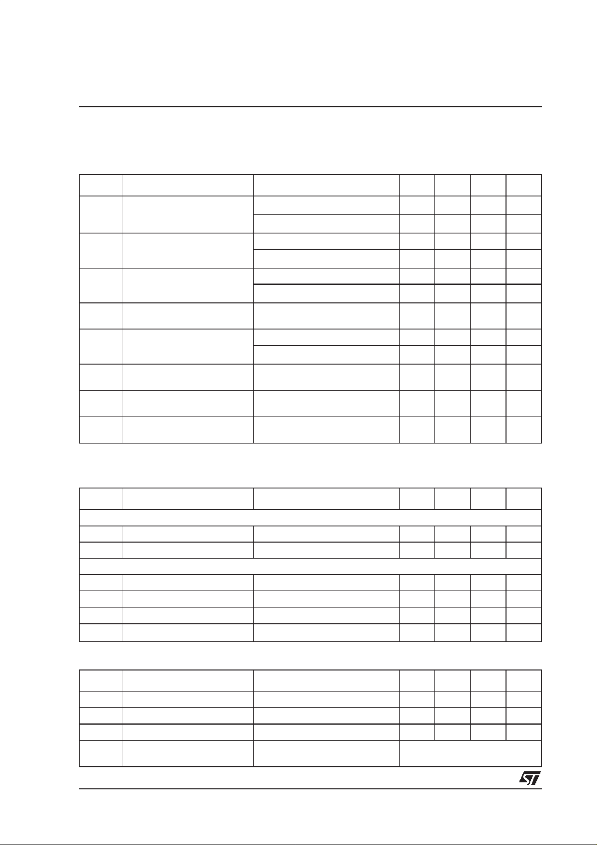
EQUIVALENT CIRCUITS
TSA0801
Figure 1 : Analog Input Circuit
AVCC = 2.5V
VIN
(orVINB)
PAD
CAPACI TANCE
7pF
AGND=0V
Figure 2 : Input clock circuit
DVCC=2.5V
CLK
commonmode
Figure 3 : Input buffers
VCCbuf=2.5V
Ω278 .5 Ω208.2Ω355.5
DFS
7pF
PAD
CAPACITANCE
GNDbuff=0V
Figure 4 : Tri-state output buffers
VCCbuf=2.5V
OE
PAD
CAPACITANCE
7pF
DGND=0V
DATA
GNDbuff=0V
GNDbuff=0V
VCCbuf =2.5V
OUT
2mA
OUTPU T
BUFFER
PAD CAPACITANCE
7pF
9/20
Page 10

TSA0801
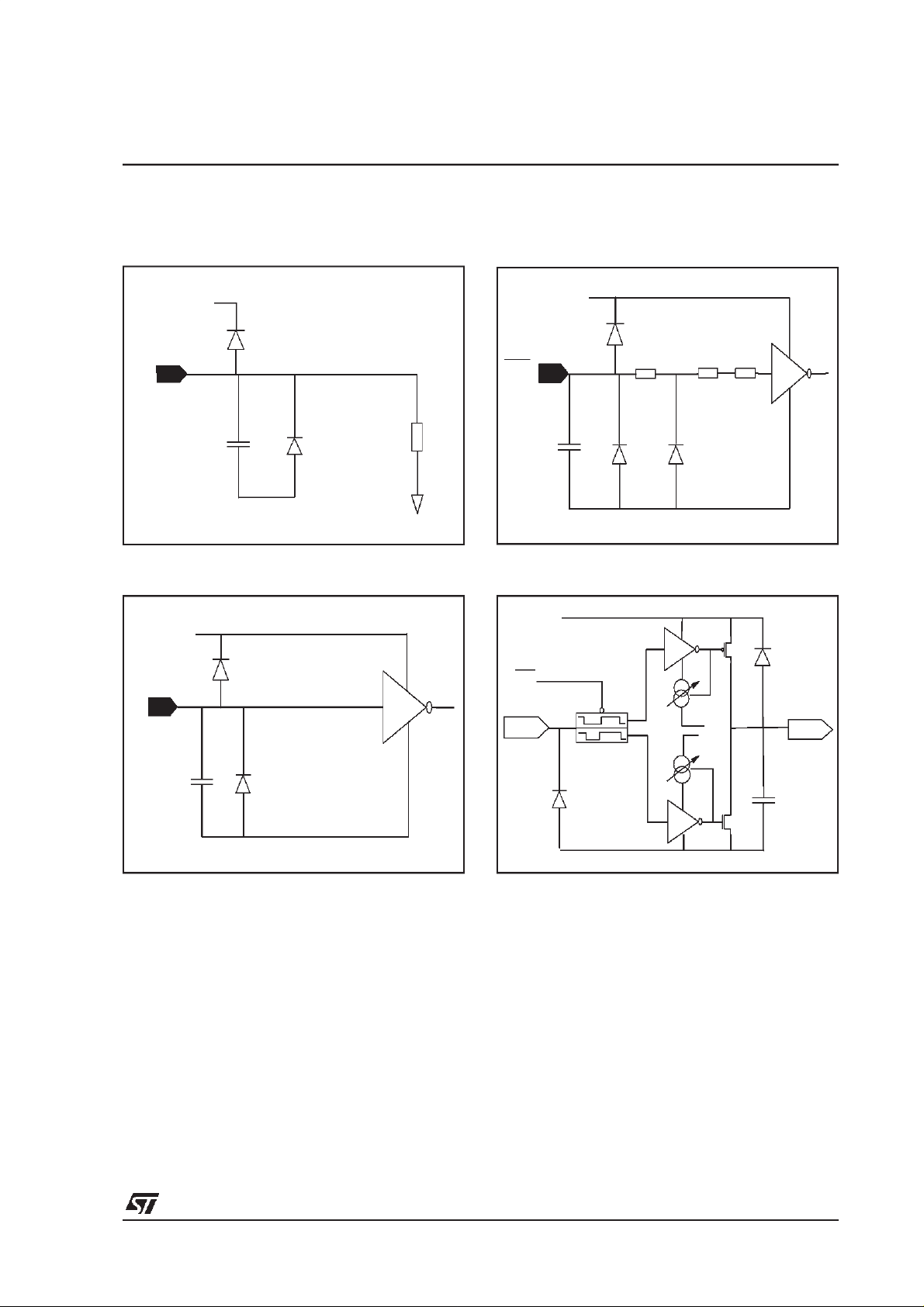
Static parameter: Integral Non Linearity
Fs=40MSPS; Fin=1MHz; Icca=11mA; N=65536pts
0.1
0.05
0
-0 .0 5
INL (LSBs)
-0. 1
-0 .1 5
0 50 100 150 200 250
Static parameter: Differential Non Linearity
Fs=40MSPS; Fin=1MHz; Icca=11mA; N=65536pts
0.08
0.06
0.04
0.02
0
-0. 0 2
DNL (LSBs)
-0. 0 4
-0. 0 6
-0. 0 8
-0 .1
0 5 0 10 0 150 2 00 25 0
Output Code
Output Code
Linearity vs. AVcc
Fs=40MSPS; Icca=11mA; Fin=1MHz
-67
-67.5
-68
-68.5
-69
-69.5
DynamicParameters(dB)
-70
2.25 2.35 2.45 2.55 2.65
10/20
THD
SFDR
AVCC(V)
Distortion vs. AVcc
Fs=40MSPS; Icca=11mA; Fin=1MHz
49.4
49.3
49.2
49.1
49
48.9
48.8
48.7
Dynamicparameters(dB)
48.6
2.25 2.35 2.45 2.55 2.6 5
SNR
SINAD
ENOB
AVCC(V)
8
7.995
7.99
7.985
7.98
7.975
7.97
7.965
7.96
7.955
7.95
ENOB (bits)
Page 11
TSA0801
Linearity vs. DVcc
Fs=40MSPS; Icca=11mA; Fin=1MHz
49.9
49.7
49.5
49.3
49.1
48.9
Dynamic parameters
48.7
48.5
2.25 2.35 2.45 2.55 2.65
SINAD
EN0B
SNR
DVCC(V)
Linearity vs. VccB
Fs=40MSPS; Icca=11mA; Fin=1MHz
50
49.9
49.8
49.7
49.6
49.5
49.4
49.3
49.2
49.1
Dynamicparameters(dB)
49
2.25 2.35 2.45 2.55 2.65
ENOB
SNR
SINAD
VCCB(V)
8
7.99
7.98
7.97
7.96
7.95
7.94
7.93
7.92
7.91
7.9
8
7.99
7.98
7.97
7.96
7.95
7.94
7.93
7.92
7.91
7.9
ENOB (bits)
ENOB (bits)
Distortion vs. DVcc
Fs=40MSPS; Icca=11mA; Fin=1MHz
-61
-63
-65
-67
-69
-71
-73
Dynamicparameters(dB)
-75
2.25 2.35 2.45 2.55 2.65
THD
SFDR
DVCC(V)
Distortion vs. VccB
Fs=40MSPS; Icca=11mA; Fin=1MHz
-65
-66
-67
-68
-69
-70
-71
-72
-73
-74
Dynamicparameters(dB)
-75
2.25 2.35 2.45 2.55 2.65
VCCB(V)
SFDR
THD
Linearity vs. Fs
Icca=11mA;Fin=5MHz
52
51.5
51
50.5
50
49.5
49
48.5
48
47.5
Dynamicparameters(dB)
47
20 30 40 50 60
SINAD
ENOB
SNR
Fs (MHz)
8
7.9
7.8
7.7
7.6
7.5
7.4
7.3
7.2
ENOB (bits)
Distortion vs. Fs
Icca=11mA;Fin=5MHz
-50
-55
-60
-65
-70
-75
Dynamicparameters(dB)
-80
20 30 40 50 60
THD
SFDR
Fs (MHz)
11/20
Page 12

TSA0801
Linearity vs. Fs
Icca=11mA;Fin=15MHz
-50
-55
-60
-65
-70
-75
-80
Dynamicparameters(dB)
-85
20 30 40 50 60
Linearity vs. Fin
Fs=40MSPS; Icca=11mA
50
49.8
49.6
49.4
49.2
49
48.8
48.6
Dynamicparameters(dB)
48.4
0 204060
SINAD
Fin (MHz)
THD
SFDR
Fs (MHz)
SNR
ENOB
8
7.95
7.9
7.85
7.8
7.75
7.7
ENOB (bits)
Distortion vs. Fs
Icca=11mA;Fin=15MHz
52
51
50
49
48
47
Dynamicparameters(dB)
46
20 30 40 50 60
Fs (MHz)
Distortion vs. Fin
Fs=40MSPS; Icca=11mA
-50
-55
-60
-65
-70
Dynamicparameters(dB)
-75
0 204060
ENOB
SNR
SINAD
THD
SFDR
Fin (MHz)
8
7.9
7.8
7.7
7.6
7.5
7.4
7.3
7.2
7.1
7
ENOB (bits)
Linearity vs. Temperature
Fs=40MSPS; Icca=11mA; Fin=5MHz
50
12/20
49.8
49.6
49.4
49.2
49
48.8
48.6
48.4
48.2
DynamicParameters(dB)
48
-50 0 50 100
Temperature(°C)
ENOB
SNR
SINAD
8
7.95
7.9
7.85
7.8
Distortion vs. Temperature
Fs=40MSPS; Icca=11mA; Fin=5MHz;
90
85
80
75
70
65
60
DynamicParameters(dB)
55
-50 0 50 100
Temperature(°C)
THD
SFDR
Page 13

Power spectrum
Fs=40MSPS - Icca=11mA - Fin=1MHz
0
-20
-40
-60
-80
Power spectrum (dBm)
-100
0246810 12 14 16 18
Power spectrum
Fs=40MSPS - Icca=11mA - Fin=10MHz
0
TSA0801
Frequency(MHz)
-20
-40
-60
-80
Power spectrum (dBm)
-100
0246810 12 14 16 18
Power spectrum
Fs=40MHz - Icca=11mA - Fin=50MSPS
0
-20
-40
-60
-80
Power spectrum (dBm)
Frequency(MHz)
-100
0246810 12 14 16 18
Frequency(MHz)
13/20
Page 14
TSA0801 APPLICATION NOTE
DETAILED INFORMATION
The TSA0801 is a High Speed analog to digital
converter basedon a pipeline architecture and the
latest deep submicron CMOS process to achieve
the best performances in terms of linearity and
power consumption.
The pipeline structure consists of 9 internal conversion stages in which the analog signal is fed
and sequentially converted into digital data.
Each 8 first stagesconsists of an Analog to Digital
converter, a Digital toAnalog converter, a Sample
and Holdand again of2amplifier. A1.5bit conversion resolution is achieved in each stage. The latest stage simply is a comparator. Each resulting
LSB-MSB couple is then time shifted to recover
from the conversion delay. Digital data correction
completes the processing by recovering from the
redundancy of the (LSB-MSB) couple for each
OPERATIONAL MODES DESCRIPTION
Inputs Outputs
Analog input differential level DFSB OEB OR DR Most Significant Bit (MSB)
(VIN-VINB) > RANGE H L H CLK D9
-RANGE > (VIN-VINB) H L H CLK D9
RANGE> (VIN-VINB) >-RANGE H L L CLK D9
(VIN-VINB) > RANGE L L H CLK Complemented D9
-RANGE > (VIN-VINB) L L H CLK Complemented D9
RANGE> (VIN-VINB) >-RANGE L L L CLK Complemented D9
XXHHZHZHZ
stage. The corrected data are outputted through
the digital buffers.
Signal input is sampled on the rising edge of the
clock while digital outputs are delivered onthe falling edge of the Data Ready signal.
The advantages of such a converter reside in the
combination of pipeline architecture and the most
advanced technologies. The highestdynamic performances are achieved while consumption remains at the lowest level.
Some functionalities have been added in order to
simplify as much as possible the application
board. These operational modes are described in
the following table.
The TSA0801 is pin to pin compatible with the
10bits/25Msps TSA1001, the 10bits/50Msps
TSA1002 and the 12bits/50Msps TSA1201. This
ensures aconformity within theproduct familyand
above all, an easy upgrade of theapplication.
Data Format Select (DFSB)
When set to low level (VIL), the digital inputDFSB
provides a two’s complement digital output MSB.
This can be ofinterest when performing some further signal processing.
When set to high level (VIH), DFSB provides a
standard binary output coding.
Output Enable (OEB)
When set to low level (VIL), all digital outputs
remain active and are in low impedance state.
When set to high level (VIH), all digital outputs
buffers are in highimpedance state.This resultsin
lower consumption while the converter goes on
sampling.
14/20
When OEB is set to low level again, the data is
then valid on the output with a very short Ton
delay.
The timing diagram summarizes this operating
cycle.
Out of Range (OR)
This function is implemented on the output stage
in order toset upan ”Out of Range” flag whenever
the digital data is over the full scale range.
Typically, there is a detection of all the data being
at ’0’ or all the data being at ’1’. This ends up with
an output signal OR which is in low level state
(VOL) when the data stay within the range, or in
high levelstate (VOH)when the dataare out of the
range.
Page 15
TSA0801
Data Ready (DR)
The Data Ready output is an image of the clock
being synchronizedon theoutput data (D0 to D9).
This is a very helpful signal thatsimplifies the synchronization of the measurement equipment or
the controlling DSP.
As digitaloutput, DRgoes in highimpedance state
when OEB is asserted to High level as described
in the timing diagram.
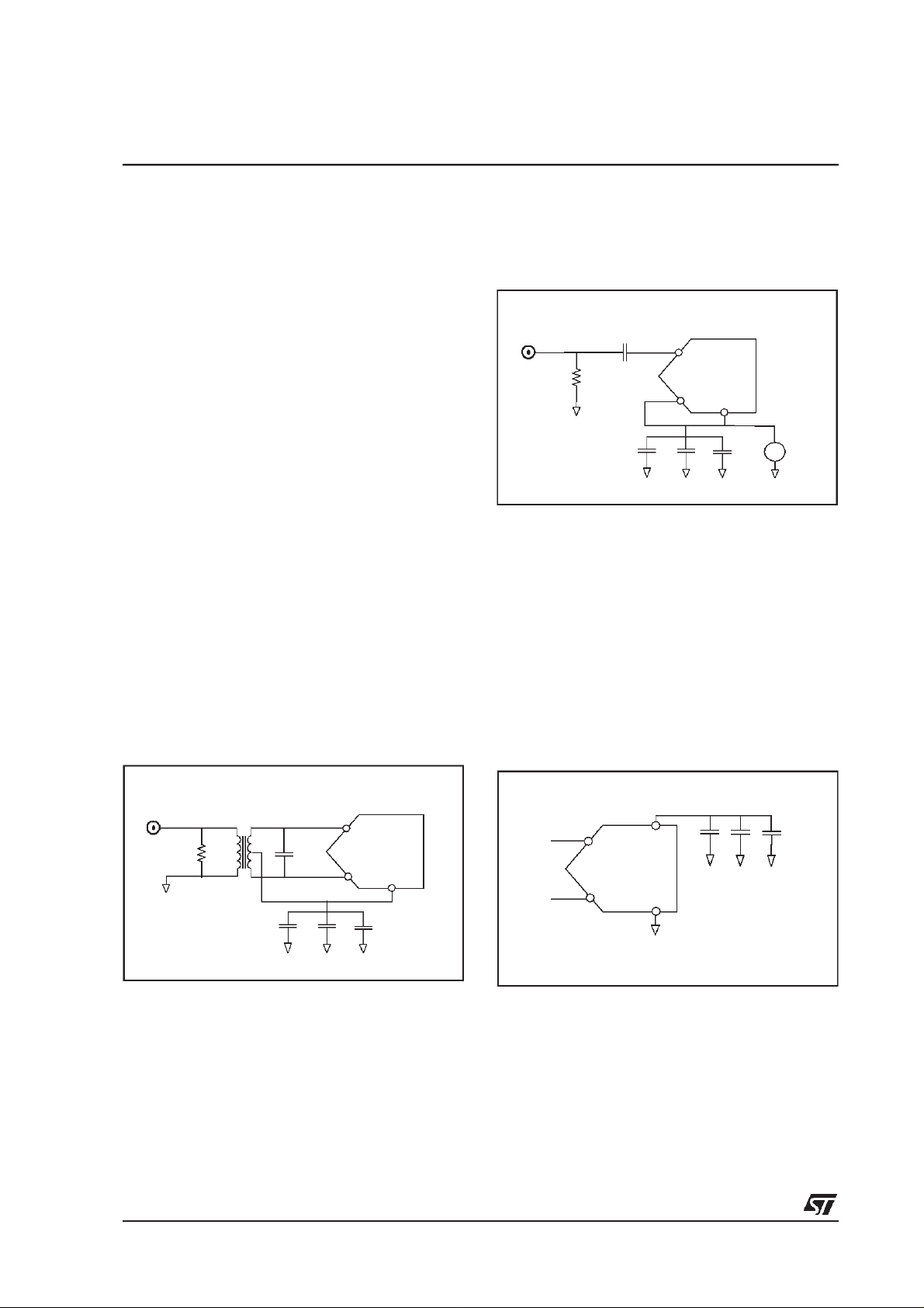
DRIVING THE ANALOG INPUT
Differential inputs
The TSA0801 has been designed to obtain optimum performances when being differentially driven. An RF transformer is a good way to achieve
such performances.
Figure 5 describes the schematics. The input signal is fed to the primary of the transformer, while
the secondary drives both ADC inputs. The common mode voltage of the ADC (INCM) is connected to the center-tap of the secondary of the transformer in order to bias the inputsignal around this
common voltage, internally set to 0.56V. The
INCM is decoupled to maintain a low noise level
on this node. Our evaluation board is mounted
with a 1:1 ADT1-1 transformer from Minicircuits.
You might also use a higher impedance ratio (1:2
or 1:4) to reduce the driving requirement on the
analog signal source.
Each analog input can drive a 1Vpp amplitude input signal, so the resultant differentialamplitude is
2Vpp.
amplitude, or it must be increased to 0.9V to
support a 2Vpp input amplitude. Performances
are better when using a 2Vpp signal.
Figure 6 : Single-ended input configuration
Signal source
50Ω
100nF
330pF
VIN
TSA0801
VINB
INCM
10nF
470nF
0.9V
REFERENCE CONNECTION
Internal reference
In the standard configuration, the ADC is biased
with the internal reference voltage. VREFM pin is
connected to Analog Ground while VREFP is internally set to a voltageof 1.03V. It is recommended to decouple the VREFP in order to minimize
low andhigh frequencynoise. Referto Figure 7 for
the schematics.
Figure 5 : Differential input configuration
Analog source
50Ω
ADT1-1
1:1
330pF
100pF
10nF
VIN
TSA0801
VINB
INCM
470nF
Single-ended input configuration
Some applications may require a single-ended
input which is easily achieved with the
configuration reported on Figure 6.
In this case, it is recommended to use an
AC-coupled analog input and connect the other
analog input to the common mode voltage of the
circuit (INCM) soas to properly bias the ADC.The
INCM may remain at the same internal level
(0.56V) thus supporting only a 1Vpp of input
Figure 7 : Internal reference setting
VIN
1.03V
VREFP
330pF
10nF
470nF
TSA0801
VINB
VREFM
External reference
It is possible to use an external reference voltage
instead of the internalone for specific applications
requiring even better linearity or enhanced
tem0801perature behavior. In this case, the
amplitude of the external voltage must be at least
equal to the internal one (1.03V). Using the
STMicroelectronics Vref TS821 leads to optimum
15/20
Page 16

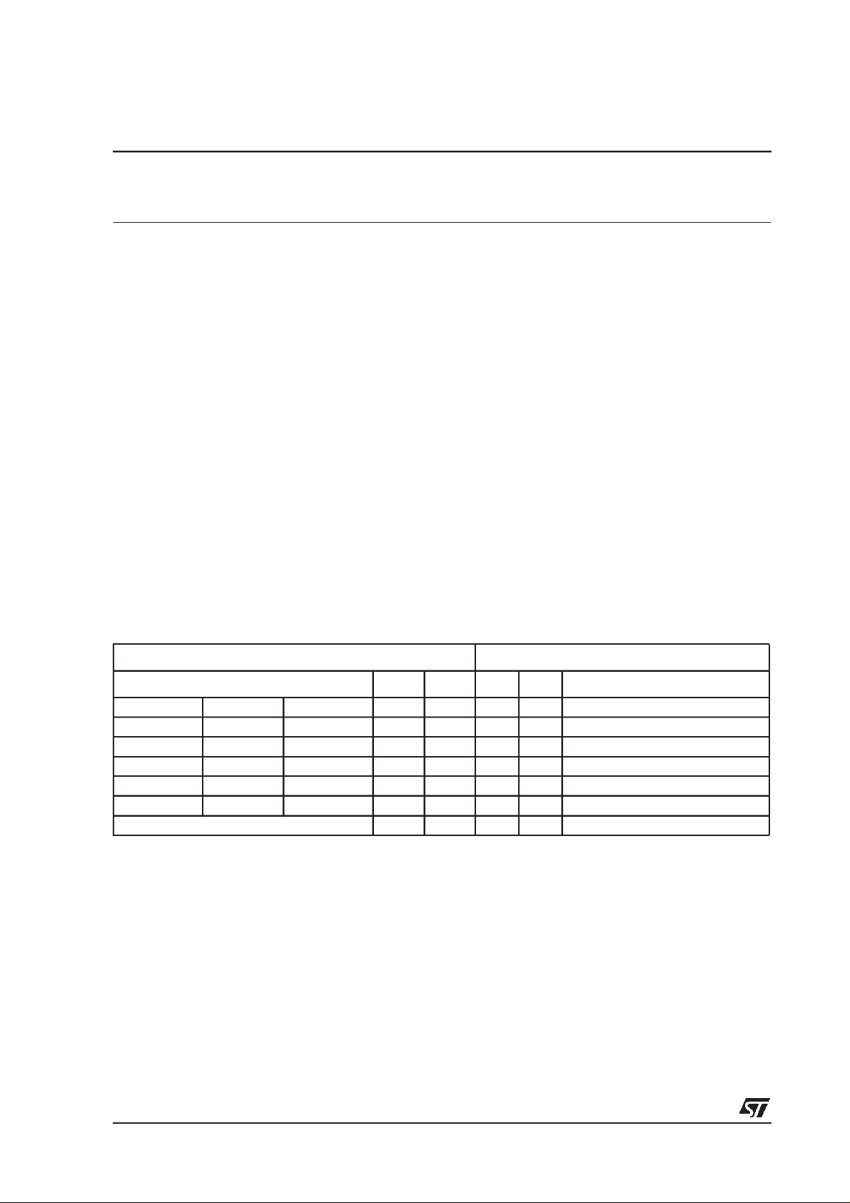
TSA0801
performances when configured as shown on
Figure 8.
Figure 8 : External reference setting
1kΩ
10nF
470nF
VCCA
VIN
TSA0801
VINB
VREFP
VREFM
330pF
TS821
external
reference
At 15Msps sampling frequency, 1MHz input frequency and -1dBFS amplitude signal, performances can be improved of up to 2dBc on SFDR
and 0.3dB on SINAD. At 40Msps sampling frequency, 1MHz inputfrequency and -1dBFS amplitude signal, performances can be improved of up
to 1dBc on SFDR and0.6dB on SINAD.
This canbe very helpful for example for multichannel application to keep a good matching among
the sampling frequency range.
Clock input
The quality ofyour converter is very dependant on
your clock input accuracy, in terms of aperture jitter; the use of low jitter crystal controlled oscillator
is recommended.
The duty cycle must be between 45% and 55%.
The clock power suppliesmust be separated from
the ADC output ones to avoid digital noise modulation at the output.
It is recommended to always keep the circuit
clocked, even at the lowest specified sampling
frequency of 0.5Msps, before applying the supply
voltages.
Power consumption optimization
The internal architecture of the TSA0801 enables
to optimize the power consumption according to
the sampling frequency of the application. For this
purpose, a resistor is placed between IPOL and
the analog Ground pins.
The TSA0801 will combine highest performances
and lowest consumption at 40Msps when Rpol is
equal to 18kΩ.
At lower sampling frequency range (< 10Msps),
this value of resistor may be adjusted in order to
decrease the analog current without any
degradation of dynamic performances.
As an example,10mW total power consumption is
achieved at 5 Msps with Rpol equelto 390kΩ.
The table below sums up the relevant data.
Total power consumption optimization
depending on Rpol value
Fs (Msps) 5 15 25 40
kΩ)
Rpol (
Optimized
power (mW)
390 40 25 18
10 25 35 40
Layout precautions
To usethe ADC circuits in thebest manner at high
frequencies, some precautions have to be taken
for power supplies:
- First of all, the implementation of 4 separate
proper supplies and ground planes (analog, digital, internal and external buffer ones) on the PCB
is mandatory for high speed circuit applications to
provide low inductance and low resistance common return.
The separation of the analog signal from the digital part is essential to prevent noise from coupling
onto the input signal.
- Power supply bypass capacitors must be placed
as close as possible to the IC pins in order to
improve high frequency bypassing and reduce
harmonic distortion. - Proper termination of all
inputs and outputs must be incorporated with
output termination resistors; then the amplifier
load will be only resistive and the stability of the
amplifier willbe improved. All leads must be wide
and as short as possible especially for the analog
input in order to decrease parasitic capacitance
and inductance.
- To keep the capacitive loading as low as
possible at digital outputs, short lead lengths of
routing are essential to minimize currents when
the output changes. To minimize this output
capacitance, buffers or latches closeto the output
pins will relax this constraint.
- Choose component sizes as small as possible
(SMD).
16/20
Page 17

TSA0801
EVAL0801 evaluation board
The characterization of the board has been made
with a fully ADC devoted test bench as shown on
Figure 10.The analog signalmust befiltered to be
very pure.
The datareadysignal isthe acquisitionclock ofthe
logic analyzer.
The ADC digital outputs are latched by the octal
buffers 74LCX573.
All characterization measurements have been
made with:
SFSR=+0.2dB for static parameters.SFSR=-0.5dB for dynamic parameters.
Figure 9 : Analog to Digital Converter characterization bench
Power
HP8644B
Sinewave
Generator
Vin
HP8133A
ADC
evaluation
board
ck
Pulse
Generator
data
dataready
Analyzer
TLA704
Logic
HP8644B
SineWave
Generator
17/20
Page 18

Figure 10 : TSA0801 evaluation board schematic
TSA0801
J17
VDDBUFF3V
J13
J11
J10
OEB
J9
DFSB
J6
123456789
DR
2
VCCB2
1
+
C34
47µ
2
1
2
1
2
1
2
1
R10
47K
R11
47K
R12
47K
R13
47K
C37
VCCB1
C28
AVCC
C16
470nF
470nF
470nF
C26
10nF
C39
C25
10nF
C27
C14
C15
10nF
Raj1
47K
R2
1011121314151617181920212223242526272829303132
D1D2D3D4D5
DO
11
12
20
LE
Q019Q118Q217Q316Q415Q514Q613Q7
VCC
U2
330pF
OEB1D02D13D24D35D46D57D68D79GND
R19
47K
R18
47K
R17
47K
R16
47K
R15
47K
R14
47K
330pF
330pF
1K
10
D0
37
DR
38
39
GNDBUFF
40
41
NC
42
NC
43
OEB
44
DFSB
45
AVCC
46
AVCC
47
AGND
48
Ipol1VrefP2VrefM3AGND4Vin5AGND6VINB7AGND8INCM9AGND10AVCC11AVCC
C11
330pF
C12
10nF
C13
470nF
C30
330pF
10nF
C31
C32
470nF
D6
D7D8D9
20
Q019Q118Q217Q316Q415Q514Q613Q7
VCC
74LCX573
OEB1D02D13D24D35D46D57D68D79GND
27D928D829D730D631D532D433D334D235D136
2.5VCCBUFF
2.5VCCBUFF
8-14bits ADC
TSA0801
D10
D11
U3
D1225D1126D10
D13
OR
2.5VCCBUFF
GNDBUFF
GNDBUFF
DGND
NC
DGND
CLK
DGND
DVCC
DVCC
12
C2
330pF
C4
10nF
C3
470nF
32PIN
OR
D13
D12
11
12
LE
C38
74LCX573
10
24
23
22
21
20
19
18
17
16
15
14
13
+
C29
43
2
6
470nF
C40
C17
10µF
T1
C20
C33
10nF
330pF
C18
T2-AT1-1WT
R3
1
330pF
C21
330pF
VCCB1
1
2
+
J18
10nF
C19
470nF
C24
50
10nF
C22
470nF
C23
VccB1
10µ
C35
47µ
J4
CLJ/SMB
1
2
J16
CON2
C36
47µ
+
1
10µ
2
J15
DVCC
AVCC
C8
330pF
C5
C1
100pF
4326
T2
T2-AT1-1WT
R1
50
1
1
2
1
VrefP
2
J5
VrefM
J1
Vin
J2
330pF
C9
10nF
C6
10nF
C10
470nF
C7
470nF
1
2
1
J7
Reglcom mode
J8
C41
10µF
C42
47µF
+
1
2
1
2
1
2
1
2
1
2
J12
AVCC
J19
AGND
J20
DGND
Mescom Mode
J21
GndB2
2
J22
GndB1
18/20
Page 19

TSA0801
Figure 11 : circuitboard - Topside silkscreen
Printed circuit board - List of components
Part Design Footprint Part Design Footprint Part Design Footprint P art Design F ootprint
Type
10u F C 2 4 1210
10u F C 2 3 1210
10u F C 4 1 1210
10u F C 2 9 1210
100 pF C 1 603
10nF C 12 603
10nF C 39 603
10nF C 15 603
10nF C 40 603
10nF C 27 603
10nF C 4 603
10nF C 21 603
10nF C 31 603
10nF C 6 603
10nF C 9 603
10nF C 18 603
1KΩR2 603
32P IN J6 IDC 32
330pF C 25 603
330pF C 26 603
19/20
ator
ator
Type
330pF C 33 603 470nF C7 805 A VCC J12 F IC HE2M M
330pF C 20 603 470nF C16 805 C LJ/SM B J4 SM B /H
330pF C 8 603 470nF C 19 805 A GND J19 F IC HE2M M
330pF C 2 603 470nF C 3 805 D FSB J9 FICHE 2MM
330pF C 5 603
330pF C 11 603
330pF C 30 603
330pF C 17 603
330pF C 14 603
47uF C36 CAP
47uF C34 CAP
47uF C35 CAP
47uF C42 CAP
470nF C 22 805
470nF C 32 805
470nF C 37 805
470nF C 38 805
470nF C 13 805 7 4LCX573 U3 TS SOP20 VrefP J2 FICHE 2M M
470nF C 28 805 74LCX 573 U2 TS SOP 20 T SA0801 U1 T QFP 48
470nF C 10 805 C ON2 J16 SIP 2
Type
47K
47K
47K
47K
47K
47K
47K
47K
47K
47K
47K
50
50
ator
Ω R 12 603 D GND J20 F ICHE2M M
Ω
R14 603 D VCC J15 F ICH E2M M
Ω R11 603 GndB1 J22 FICHE2MM
Ω
R a j1 V R 5 G ndB 2 J2 1 F IC HE 2 M M
Ω R10 603 Mes commode J8 FICHE2MM
Ω
R19 603 OEB J10 FICHE2MM
Ω R 13 603 R egl com m ode J7 F ICHE2M M
Ω
R15 603 T2-AT1-1WT T2 ADT
Ω
R16 603 T2-AT1-1WT T1 ADT
Ω
R17 603 VccB 1 J18 F ICHE 2M M
Ω
R18 603 VDDBUFF3V J17 FICHE2MM
Ω
R3 603 V in J1 SM B /H
Ω
R1 603 V refM J5 F ICHE2M M
Type
ato r
Page 20

PACKAGE MECHANICAL DATA:
48 PINS - PLASTIC PACKAGE
48 37
1
TSA0801
A
A2
e
A1
0,10 mm
.004 inch
36
E3
E1
SEATING PLANE
B
E
12
13 24
D3
25
c
D1
D
L1
L
0,25 mm
.010 inch
K
Millimeters Inches
Dim.
Min. Typ. Max. Min. Typ. Max.
A 1.60 0.063
A1 0.05 0.15 0.002 0.006
A2 1.35 1.40 1.45 0.053 0.055 0.057
B 0.17 0.22 0.27 0.007 0.009 0.011
C 0.09 0.20 0.004 0.008
D 9.00 0.354
D1 7.00 0.276
D3 5.50 0.216
e 0.50 0.0197
E 9.00 0.354
E1 7.00 0.276
E3 5.50 0.216
L 0.45 0.60 0.75 0.018 0.024 0.030
L1 1.00 0.039
K0°(min.), 7° (max.)
Information furnished is believed to be accurate and reliable. However, STMicroelectronics assumes no responsibility for the
consequences of use ofsuch information norfor any infringement of patents or other rights of third parties which may result from
its use. No license is granted by implication or otherwise under any patent or patent rights of STMicroelectronics. Specifications
mentioned in this publication are subject to change without notice. This publication supersedes and replaces all information
previously supplied. STMicroelectronics products are not authorized for use as critical components in life support devices or
systems withoutexpress written approval of STMicroelectronics.
The ST logo is a registered trademark of STMicroelectronics
GAGE PLANE
2000 STMicroelectronics - Printed in Italy - All Rights Reserved
STMicroelectronics GROUP OF COMPANIES
Australia - Brazil - China - Finland -France - Germany - Hong Kong - India - Italy - Japan - Malaysia - Malta - Morocco
Singapore - Spain - Sweden - Switzerland - United Kingdom
http://www.st.com
20/20
 Loading...