

Datasheet TS9006DCQ6, TS9006DCU4, TS9006DCX5, TS9006KCQ6, TS9006KCU4 Datasheet (TSC) [ru]
...Page 1
TS9006
150mA Low Noise CMOS LDO
1/9 Version: A07
SOT-343
SOT-25
DFN 2x2
General Description
TS9006 series is 150mA low-noise CMOS LDO especially designed for battery-power RF and wireless applications.
The TS9006 regulator achieves a low 250mV dropout at 150mA load current of 3.3V output, ultra-low output voltage
noise of 15uVrms and PSRR of 57dB at 1KHz.TS9006 regulators are also optimized to work with low-ESR and low
cost ceramic capacitors reducing the amount of board space critical in hand-held devices. The TS9006 requires only
0.47uF output capacitor for stability with and load. The TS9006 consumes less than 1uA in shutdown mode.
Features
● 250mV Dropout at 150mA load (3.3V)
● Quiescent current: 90µA (typ.)
● Output voltage ±2%
● Internal current limit and thermal shutdown
● Power saving shutdown mode (<1uA)
● Only need input and output capacitors
● Build-In internal Soft-Start
● Output short-circuit current limit protection
Ordering Information
Note: Where x denotes voltage option, available are
D= 1.8, K= 2.5V, M= 2.7V, N= 2.8V, P= 3.0V,
S= 3.3V
Contact factory for additional voltage options.
Part No.
Package
Packing
TS9006xCX5 RF
SOT-25
3Kpcs / 7” Reel
TS9006xCU4 RF
SOT-343
3Kpcs / 7” Reel
TS9006xCQ6 RF
DFN 2x2
3Kpcs / 7” Reel
Applications
● Palmtops, PDA and Notebook Computers
● DSC, Handset Camera Modules
● PCMCIA Cards, PC Cameras
● USB Based Portable Devices (MPS, PMP)
● GSM/GPRS/3G RF Transceiver Modules
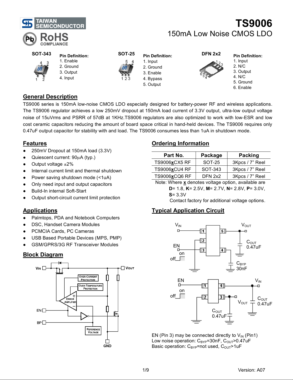
Block Diagram
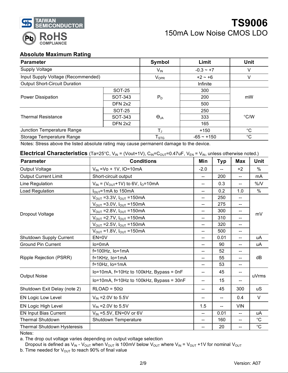
Typical Application Circuit
EN (Pin 3) may be connected directly to VIN (Pin1)
Low noise operation: C
BYP
=30nF, C
OUT
>0.47uF
Basic operation: C
BYP
=not used, C
OUT
>1uF
Pin Definition:
1. Enable
2. Ground
3. Output
4. Input
Pin Definition:
1. Input
2. Ground
3. Enable
4. Bypass
5. Output
VIN
V
OUT
C
OUT
0.47uF
C
BYP
30nF
on
off
EN
V
OUT
VIN
EN
on
off
C
OUT
0.47uF
C
OUT
0.47uF
Pin Definition:
1. Input
2. N/C
3. Output
4. N/C
5. Ground
6. Enable
Page 2
TS9006
150mA Low Noise CMOS LDO
2/9 Version: A07
Absolute Maximum Rating
Parameter
Symbol
Limit
Unit
Supply Voltage
VIN
-0.3 ~ +7
V
Input Supply Voltage (Recommended)
V
OPR
+2 ~ +6
V
Output Short-Circuit Duration
Infinite
SOT-25
300
SOT-343
200
Power Dissipation
DFN 2x2
PD
500
mW
SOT-25
250
SOT-343
333
Thermal Resistance
DFN 2x2
ӨJA
165
°C/W
Junction Temperature Range
TJ
+150
°C
Storage Temperature Range
T
STG
-65 ~ +150
°C
Notes: Stress above the listed absolute rating may cause permanent damage to the device.
Electrical Characteristics (Ta=25°C, V
IN
= (Vout+1V), CIN=C
OUT
=0.47uF, VEN = VIN, unless otherwise noted.)
Parameter
Conditions
Min
Typ
Max
Unit
Output Voltage
VIN =Vo + 1V, IO=10mA
-2.0
--
+2
%
Output Current Limit
Short-circuit output
--
200
--
mA
Line Regulation
VIN = (V
OUT
+1V) to 6V, IO=10mA
--
0.3
--
%/V
Load Regulation
I
OUT
=1mA to 150mA
--
0.2
1.0
%
V
OUT
=3.3V, I
OUT
=150mA
--
250
--
V
OUT
=3.0V, I
OUT
=150mA
--
275
--
V
OUT
=2.8V, I
OUT
=150mA
--
300
--
V
OUT
=2.7V, I
OUT
=150mA
--
310
--
V
OUT
=2.5V, I
OUT
=150mA
--
320
--
Dropout Voltage
V
OUT
=1.8V, I
OUT
=150mA
--
500
--
mV
Shutdown Supply Current
EN=0V
--
0.01
--
uA
Ground Pin Current
Io=0mA
--
90
--
uA
f=100Hz, Io=1mA
--
52
--
f=1KHz, Io=1mA
--
55
--
Ripple Rejection (PSRR)
f=10Hz, Io=1mA
--
53
--
dB
Io=10mA, f=10Hz to 100kHz, Bypass = 0nF
--
45
--
Output Noise
Io=10mA, f=10Hz to 100kHz, Bypass = 30nF
--
15
--
uVrms
Shutdown Exit Delay (note 2)
RLOAD = 50Ω
--
45
300
uS
EN Logic Low Level
VIN =2.0V to 5.5V
--
--
0.4
V
EN Logic High Level
VIN =2.0V to 5.5V
1.5
--
VIN
EN Input Bias Current
VIN =5.5V, EN=0V or 6V
--
0.01
--
uA
Thermal Shutdown
Shutdown Temperature
--
160
--
°C
Thermal Shutdown Hysteresis
--
20
--
°C
Notes:
a. The drop out voltage varies depending on output voltage selection
Dropout is defined as VIN - V
OUT
when V
OUT
is 100mV below V
OUT
where VIN = V
OUT
+1V for nominal V
OUT
b. Time needed for V
OUT
to reach 90% of final value
Page 3
TS9006
150mA Low Noise CMOS LDO
3/9 Version: A07
Application Information
Enable / Shutdown
The TS9006 comes with and active-high enable pin that allows the regulator to be enabled. Forcing the enable pin low
disables the regulator and puts it into the shutdown mode. This pin cannot be left floating as it may cause an
undetermined state.
Input / Output Capacitor
It is recommended to use a 0.47uF capacitor on the TS9006 input and a 0.47uF capacitor on the output. For high
regulation performance, larger input capacitor values and lower ESRs provide better noise rejection and line-transient
response. The output noise, load-transient response, stability, and power-supply rejection can be improved by using
large output capacitors. Low ESR ceramic capacitors provide optimal performance and save space.
Power Supply Rejection and Transient Response
The PSRR and transient response can be improved by increasing the values of the input and output bypass
capacitors, and through passive filtering techniques
Functional Description
Description
The TS9006 is an ultra-low-noise, low-quiescent current, low-dropout linear regulator. It is supplied in a SOT-25,
SOT-343 & DFN 2x2 package for difference applications. This device can supply loads up to 150mA. As shown in the
functional block diagram, the TS9006 consists of a reference and noise bypass circuit, error amplifier, output drive
transistor, internal feedback voltage divider, thermal sensor, and short circuit current limiter. The internal reference is
connected to the error amplifier’s inverting input. The error amplifier compares this reference with the feedback voltage
and amplifies the difference. If the feedback voltage is lower than the reference voltage, the pass=transistor gate is
pulled low. This allows more current to pass to the output and increases the output voltage.
Stability
The TS9006 is a high performance LDO emphasizing stability with low output capacitance. It is able to maintain
stability with an output capacitor can also be increased to optimize performance. The TS9006 will remain stable and in
regulation with no load, unlike many other voltage regulators.
Internal P-Channel Pass Transistor
The TS9006 features allow impedance P-channel MOSFET pass transistor. This provides several advantages over
similar designs using a PNP pass transistor, including low operating power and longer battery life. The TS9006
consumes only 90µA of quiescent current under most conditions.
Output Short-Circuit Current Limit
The TS9006 includes a current limiter, which monitors and controls the pass transistor’s gage voltage, limiting the
output current to about 200mA, for example, in a short-circuit output situation.
Shutdown
The TS9006 also features a low-power active shutdown mode. It has a switch that turns off the device when disabled.
This allows the output capacitor and load to discharge and de-energize the load. In the shutdown mode, the internal
functional blocks, such as voltage reference and the error amplifier, are turned off completely, and the quiescent
current is less than 1µA.
Page 4

TS9006
150mA Low Noise CMOS LDO
4/9 Version: A07
Functional Description (Continue)
Thermal Protection Shutdown
The thermal protection shutdown function protects the device from operating in over temperature condition. When the
junction temperature exceeds +160°C, the thermal sensor signals the shutdown logic, turning off the pass transistor
and allowing the IC to tool down. The thermal sensor turns the pass transistor on again after the IC’s junction
temperature drops to +140°C.
Soft-Start Circuitry
The TS9006 includes a soft-start circuitry to limit inrush current at turn-on. During power up, the output capacitor and
output load are charged with a reduce output current. Shortly after the initial power up, the soft-start feature is
terminated and normal operation is resumed.
Page 5

TS9006
150mA Low Noise CMOS LDO
5/9 Version: A07
Electrical Characteristics Curve
Dropout Voltage vs. Load Current
Dropout Voltage vs. Temperature
Ground Current vs. Input Voltage
Output Voltage vs. Temperature
PSRR vs. Frequency
PSRR vs. Frequency
Page 6

TS9006
150mA Low Noise CMOS LDO
6/9 Version: A07
SOT-25 Mechanical Drawing
Marking Diagram
A
= Device Code
X
= Fixed Output Voltage Code
D=1.8V, K=2.5V, M=2.7V, N=2.8V, P=3.0V, S=3.3V
Y
= Year Code
M
= Month Code
(A=Jan, B=Feb, C=Mar, D=Apl, E=May, F=Jun, G=Jul, H=Aug,
I=Sep, J=Oct, K=Nov, L=Dec)
L
= Lot Code
SOT-25 DIMENSION
MILLIMETERS
INCHES
DIM
MIN
MAX
MIN
MAX.
A+A1
0.09
1.25
0.0354
0.0492
B
0.30
0.50
0.0118
0.0197
C
0.09
0.25
0.0035
0.0098
D
2.70
3.10
0.1063
0.1220
E
1.40
1.80
0.0551
0.0709
E
1.90 BSC
0.0748 BSC
H
2.40
3.00
0.09449
0.1181
L
0.35 BSC
0.0138 BSC
Ө1
0º
10º
0º
10º
S1
0.95 BSC
0.0374 BSC
Page 7

TS9006
150mA Low Noise CMOS LDO
7/9 Version: A07
DFN 2x2 Mechanical Drawing
Marking Diagram
A
= Device Code
X
= Fixed Output Voltage Code
D=1.8V, K=2.5V, M=2.7V, N=2.8V, P=3.0V, S=3.3V
Y
= Year Code
M
= Month Code
(A=Jan, B=Feb, C=Mar, D=Apl, E=May, F=Jun, G=Jul, H=Aug,
I=Sep, J=Oct, K=Nov, L=Dec)
L
= Lot Code
DFN 2x2 DIMENSION
MILLIMETERS
INCHES
DIM
MIN
MAX
MIN
MAX
A
0.25
0.35
0.0098
0.0138
a1
0.10 (typ)
0.0039 (typ)
B
0.90
1.10
0.0354
0.0433
C
0.50 (typ)
0.0197 (typ)
D
0.50 (typ)
0.0197 (typ)
E
0.15
0.25
0.0059
0.0098
F
1.30
1.50
0.0512
0.0591
G
0.67
0.73
0.0264
0.0287
H
0.20
0.30
0.0079
0.0118
I
0.60 (MAX.)
0.0236 (MAX.)
J
0.07 (MAX.)
0.0028 (MAX.)
K
1.75
1.85
0.0689
0.0728
L
1.95
2.05
0.0768
0.0807
Page 8

TS9006
150mA Low Noise CMOS LDO
8/9 Version: A07
SOT-343 Mechanical Drawing
SOT-343 DIMENSION
MILLIMETERS
INCHES
DIM
MIN
MAX
MIN
MAX
A
1.80
2.20
0.0709
0.0866
B
0.25
0.40
0.0098
0.0157
C
1.30(typ)
0.0512(typ)
D
1.15
1.35
0.0453
0.0531
E
1.80
2.40
0.0709
0.0945
F
0.35
0.50
0.0137
0.0197
G
0.80
1.10
0.0315
0.0433
H
0.10
0.45
0.0039
0.0177
Page 9

TS9006
150mA Low Noise CMOS LDO
9/9 Version: A07
Notice
Specifications of the products displayed herein are subject to change without notice. TSC or anyone on its behalf,
assumes no responsibility or liability for any errors or inaccuracies.
Information contained herein is intended to provide a product description only. No license, express or implied, to any
intellectual property rights is granted by this document. Except as provided in TSC’s terms and conditions of sale for
such products, TSC assumes no liability whatsoever, and disclaims any express or implied warranty, relating to sale
and/or use of TSC products including liability or warranties relating to fitness for a particular purpose, merchantability,
or infringement of any patent, copyright, or other intellectual property right.
The products shown herein are not designed for use in medical, life-saving, or life-sustaining applications. Customers
using or selling these products for use in such applications do so at their own risk and agree to fully indemnify TSC for
any damages resulting from such improper use or sale.
Page 10

 Loading...