

Page 1
TS79M00 series
3-Terminal Medium Current Negative Voltage Regulator
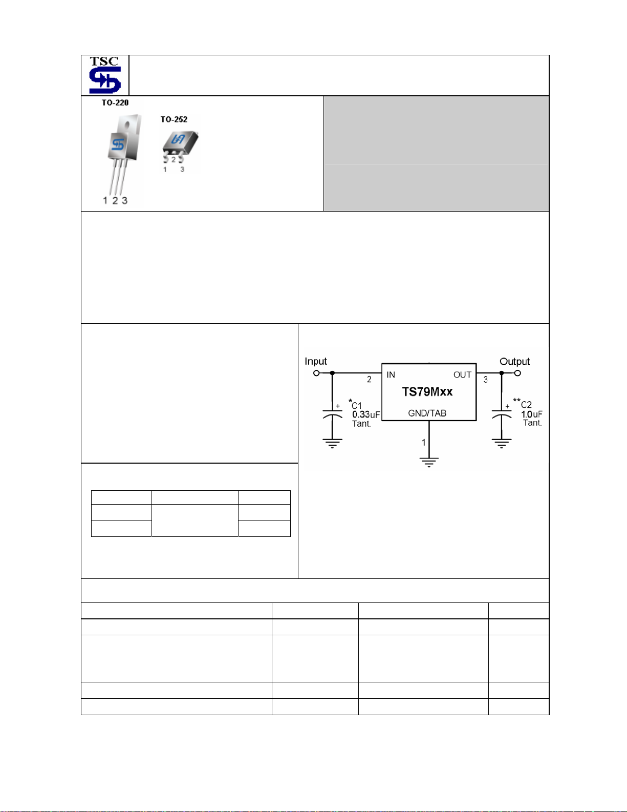
Pin assignment:
(Heatsink surface
connected to Pin 2)
1. Ground
2. Input
3. Output
Voltage Range - 5V to - 24V
Output Current up to 0.5A
General Description
The TS79M00 Series negative voltage regulators are identical to the popular TS7900 Series devices, except that they are
specified for only half the output current. Like the TS7900 devices, the TS79M00 Series 3-Terminal regulators are
intended for local, on-card voltage regulation.
Internal current limiting, thermal shutdown circuitry and safe-area compensation for the internal pass transistor combine
to make these devices remarkably rugged under most operating conditions. Maximum output current with adequate
heatsink is 500mA
This series is offered in 3-pin TO-220, TO-252 package.
Features
Output current up to 0.5A
No external components required
Internal thermal overload protection
Internal short-circuit current limiting
Output transistor safe-area compensation
Standard Application
Output voltage offered in 4% tolerance
Ordering Information
Part No. Operating Temp. Package
TS79MxxCZ TO-220
TS79MxxCP
Note: Where xx denotes voltage option.
-20 ~ +125
o
C
TO-252
A common ground is required between the input and the
output voltages. The input voltage must remain typically 2.0V
above the output voltage even during the low point on the
Input ripple voltage.
XX = these two digits of the type number indicate voltage.
* = Cin is required if regulator is located an appreciable
distance from power supply filter.
** = Co is not needed for stability; however, it does improve
transient response.
Absolute Maximum Rating
Input Voltage Vin * - 35 V
Input Voltage Vin ** - 40 V
Power Dissipation TO-220
TO-220
TO-252
Operating Junction Temperature Range TJ -20 ~ +125 oC
Storage Temperature Range T
Note : * TS79M05 to TS79M18
** TS79M24
*** Follow the derating curve
Without heatsink
Pt ***
Without heatsink
-65 ~ +150 oC
STG
2
15
1
W
TS79M00 series 1-7 2003/12 rev. A
Page 2

TS79M05 Electrical Characteristics
(Vin= -10V, Iout=350mA, 0 oC≤Tj≤125 oC, Cin=0.33uF, Cout=0.1uF; unless otherwise specified.)
Parameter Symbol Test Conditions Min Typ Max Unit
Tj=25 oC - 4.80 - 5 - 5.20
Output voltage Vout
-7.5V≤Vin≤ -20V,
- 4.75 - 5 - 5.25
5mA≤Iout≤350mA, PD≤5W
Line Regulation REGline Tj=25 oC
Load Regulation REGload Tj=25 oC
-7.5V≤Vin≤ -25V,
Io=200mA
5mA≤Iout≤500mA -- 20 100
5mA≤Iout≤200mA -- 10 50
-- 3 50
Quiescent Current Iq Iout=0, Tj=25 oC -- 4 8
Quiescent Current Change
∆Iq
-7.5V≤Vin≤ -25V -- -- 0.5
5mA≤Iout≤350mA -- -- 0.5
Output Noise Voltage Vn 10Hz≤f≤100KHz, Tj=25 oC -- 40 -- uV
Ripple Rejection Ratio RR f=120Hz, -8V≤Vin≤ -18V 54 66 -- dB
Voltage Drop Vdrop Iout=350mA, Tj=25 oC -- 2 -- V
Peak Output Current Io peak Tj=25 oC -- 0.7 -- A
Temperature Coefficient of
Output Voltage
∆Vout/ ∆Tj
Iout=5mA, 0
o
C≤Tj≤125 oC -- -0.2 --
V
mV
mA
mV/
o
C
TS79M06 Electrical Characteristics
(Vin= -11V, Iout=350mA, 0 oC≤Tj≤125 oC, Cin=0.33uF, Cout=0.1uF; unless otherwise specified.)
Parameter Symbol Test Conditions Min Typ Max Unit
Tj=25 oC - 5.75 - 6 - 6.25
Output Voltage Vout
-8.5V≤Vin≤ -21V,
- 6.3 - 6 - 6.3
5mA≤Iout≤350mA, PD≤5W
Line Regulation REGline Tj=25 oC
Load Regulation REGload Tj=25 oC
-8.5V≤Vin≤ -25V,
Io=200mA
5mA≤Iout≤500A -- 20 120
5mA≤Iout≤200mA -- 10 60
-- 3 50
Quiescent Current Iq Iout=0, Tj=25 oC -- 4 8
Quiescent Current Change
∆Iq
-8.5V≤Vin≤ -25V -- -- 0.5
5mA≤Iout≤350mA -- -- 0.5
Output Noise Voltage Vn 10Hz≤f≤100KHz, Tj=25 oC -- 40 -- uV
Ripple Rejection Ratio RR f=120Hz, -9V≤Vin≤ -19V 54 66 -- dB
Voltage Drop Vdrop Iout=350mA, Tj=25 oC -- 2 -- V
Peak Output Current Io peak Tj=25 oC -- 0.7 -- A
Temperature Coefficient of
Output Voltage
∆Vout/ ∆Tj
Iout=5mA, 0
o
C≤Tj≤125 oC -- -0.2 --
z Pulse testing techniques are used to maintain the junction temperature as close to the ambient temperature as
possible, and thermal effects must be taken into account separately.
z This specification applies only for DC power dissipation permitted by absolute maximum ratings.
V
mV
mA
mV/
o
C
TS79M00 series 2-7 2003/12 rev. A
Page 3

TS79M08 Electrical Characteristics
(Vin= -14V, Iout=350mA, 0 oC≤Tj≤125 oC, Cin=0.33uF, Cout=0.1uF; unless otherwise specified.)
Parameter Symbol Test Conditions Min Typ Max Unit
Tj=25 oC - 7.69 - 8 - 8.32
Output Voltage Vout
Line Regulation REGline Tj=25 oC
Load Regulation REGload Tj=25 oC
Quiescent Current Iq Iout=0, Tj=25 oC -- 4 8
Quiescent Current Change
Output Noise Voltage Vn 10Hz≤f≤100KHz, Tj=25 oC -- 60 -- uV
Ripple Rejection Ratio RR f=120Hz, -11V≤Vin≤ -21V 54 63 -- dB
Voltage Drop Vdrop Iout=350mA, Tj=25 oC -- 2 -- V
Peak Output Current Io peak Tj=25 oC -- 0.7 -- A
Temperature Coefficient of
Output Voltage
∆Iq
∆Vout/ ∆Tj
-10.5V≤Vin≤ -23V,
5mA≤Iout≤350mA, PD≤5W
-10.5V≤Vin≤ -25V,
Io=200mA
5mA≤Iout≤500mA -- 25 160
5mA≤Iout≤200mA -- 10 80
-10.5V≤Vin≤ -25V -- -- 0.5
5mA≤Iout≤350mA -- -- 0.5
Iout=5mA, 0
o
C≤Tj≤125 oC -- -0.4 --
- 7.61 - 8 - 8.40
-- 6 50
V
mV
mA
mV/
o
C
TS79M09 Electrical Characteristics
(Vin= -15V, Iout=350mA, 0 oC≤Tj≤125 oC, Cin=0.33uF, Cout=0.1uF; unless otherwise specified.)
Parameter Symbol Test Conditions Min Typ Max Unit
Tj=25 oC - 8.65 - 9 - 9.36
Output Voltage Vout
Line Regulation REGline Tj=25 oC
Load Regulation REGload Tj=25 oC
Quiescent Current Iq Iout=0, Tj=25 oC -- 4 8
Quiescent Current Change
Output Noise Voltage Vn 10Hz≤f≤100KHz, Tj=25 oC -- 60 -- uV
Ripple Rejection Ratio RR f=120Hz, -12V≤Vin≤ -22V 54 63 -- dB
Voltage Drop Vdrop Iout=350mA, Tj=25 oC -- 2 -- V
Peak Output Current Io peak Tj=25 oC -- 0.7 -- A
Temperature Coefficient of
Output Voltage
z Pulse testing techniques are used to maintain the junction temperature as close to the ambient temperature as
possible, and thermal effects must be taken into account separately.
z This specification applies only for DC power dissipation permitted by absolute maximum ratings.
∆Iq
∆Vout/ ∆Tj
-11.5V≤Vin≤ -23V,
5mA≤Iout≤350mA, PD≤5W
-11.5V≤Vin≤ -26V
Io=200mA
5mA≤Iout≤500mA -- 25 180
5mA≤Iout≤200mA -- 10 90
-11.5V≤Vin≤ -26V -- -- 0.5
5mA≤Iout≤350mA -- -- 0.5
Iout=5mA, 0
o
C≤Tj≤125 oC -- -0.4 --
- 8.57 - 9 - 9.45
-- 6 50
V
mV
mA
mV/
o
C
TS79M00 series 3-7 2003/12 rev. A
Page 4
TS79M12 Electrical Characteristics
(Vin= -19V, Iout=350mA, 0 oC≤Tj≤125 oC, Cin=0.33uF, Cout=0.1uF; unless otherwise specified.)
Parameter Symbol Test Conditions Min Typ Max Unit
Tj=25 oC - 11.53 - 12 - 12.48
Output Voltage Vout
-14.5V≤Vin≤ -27V,
- 11.42 - 12 - 12.60
5mA≤Iout≤350mA, PD ≤5W
Line Regulation REGline Tj=25 oC
Load Regulation REGload Tj=25 oC
-14.5V≤Vin≤ -30V,
Io=200mA
5mA≤Iout≤500mA -- 25 240
0mA≤Iout≤200mA -- 10 120
-- 8 50
Quiescent Current Iq Tj=25 oC, Iout=0 -- 4 8
Quiescent Current Change
∆Iq
-14.5V≤Vin≤ -30V -- -- 0.5
5mA≤Iout≤200mA -- -- 0.5
Output Noise Voltage Vn 10Hz≤f≤100KHz, Tj=25 oC -- 70 -- uV
Ripple Rejection Ratio RR f=120Hz, -15V≤Vin≤ -25V 54 60 -- dB
Voltage Drop Vdrop Iout=350mA, Tj=25 oC -- 2 -- V
Peak Output Current Io peak Tj=25 oC -- 0.7 -- A
Temperature Coefficient of
Output Voltage
∆Vout/ ∆Tj
Iout=5mA, 0
o
C≤Tj≤125 oC -- -0.8 --
V
mV
mA
mV/
o
C
TS79M15 Electrical Characteristics
(Vin= -23V, Iout=350mA, 0 oC≤Tj≤125 oC, Cin=0.33uF, Cout=0.1uF; unless otherwise specified.)
Parameter Test Conditions Min Typ Max Unit
Tj=25 oC - 14.42 - 15 - 15.60
Output Voltage Vout
-17.5V≤Vin≤ -30V,
- 14.28 - 15 - 15.75
5mA≤Iout≤350mA, PD ≤5W
Line Regulation REGline
Load Regulation REGload
Tj=25
o
C
Tj=25
o
C
-17.5V≤Vin≤ -30V,
Io=200mA
5mA≤Iout≤500mA -- 25 300
5mA≤Iout≤200mA -- 10 150
-- 8 50
Quiescent Current Iq Tj=25 oC, Iout=0 -- 5 8
Quiescent Current Change
∆Iq
-17.5V≤Vin≤ -30V -- -- 0.5
5mA≤Iout≤350mA -- -- 0.5
Output Noise Voltage Vn 10Hz≤f≤100KHz, Tj=25 oC -- 90 -- uV
Ripple Rejection Ratio RR f=120Hz, -18V≤Vin≤ -28V 54 60 -- dB
Voltage Drop Vdrop Iout=350mA, Tj=25 oC -- 2 -- V
Peak Output Current Io peak Tj=25 oC -- 0.7 -- A
Temperature Coefficient of
Output Voltage
∆Vout/ ∆Tj
Iout=5mA, 0
o
C≤Tj≤125 oC -- -1.0 --
z Pulse testing techniques are used to maintain the junction temperature as close to the ambient temperature as
possible, and thermal effects must be taken into account separately.
z This specification applies only for DC power dissipation permitted by absolute maximum ratings.
V
mV
mA
mV/
o
C
TS79M00 series 4-7 2003/12 rev. A
Page 5

TS79M18 Electrical Characteristics
(Vin= -27V, Iout=350mA, 0 oC≤Tj≤125 oC, Cin=0.33uF, Cout=0.1uF; unless otherwise specified.)
Parameter Symbol Test Conditions Min Typ Max Unit
Tj=25 oC - 17.30 - 18 - 18.72
Output Voltage Vout
Line Regulation REGline Tj=25 oC
Load Regulation REGload Tj=25 oC
Quiescent Current Iq Tj=25 oC, Iout=0 -- 5 8
Quiescent Current Change
Output Noise Voltage Vn 10Hz≤f≤100KHz, Tj=25 oC -- 110 -- uV
Ripple Rejection Ratio RR f=120Hz, -21V≤Vin≤ -31V 54 60 -- dB
Voltage Drop Vdrop Iout=350mA, Tj=25 oC -- 2 -- V
Peak Output Current Io peak Tj=25 oC -- 0.7 -- A
Temperature Coefficient of
Output Voltage
∆Iq
∆Vout/ ∆Tj
-21V≤Vin≤ -33V,
5mA≤Iout≤350mA, PD ≤5W
-21V≤Vin≤ -33V,
Io=200mA
5mA≤Iout≤500mA -- 25 360
5mA≤Iout≤200mA -- 10 180
-21V≤Vin≤ -33V -- -- 0.5
5mA≤Iout≤350nA -- -- 0.5
Iout=5mA, 0
o
C≤Tj≤125 oC -- -1.0 --
- 17.14 - 18 - 18.90
-- 8 50
V
mV
mA
mV/
o
C
TS79M24 Electrical Characteristics
(Vin=- 33V, Iout=350mA, 0 oC≤Tj≤125 oC, Cin=0.33uF, Cout=0.1uF; unless otherwise specified.)
Parameter Symbol Test Conditions Min Typ Max Unit
Tj=25 oC - 23.07 - 24 - 24.96
Output Voltage Vout
Line Regulation REGline Tj=25 oC
Load Regulation REGload Tj=25 oC
Quiescent Current Iq Iout=0, Tj=25 oC -- 5 9
Quiescent Current Change
Output Noise Voltage Vn 10Hz≤f≤100KHz, Tj=25 oC -- 170 -- uV
Ripple Rejection Ratio RR f=120Hz, -27V≤Vin≤ -37V 50 60 -- dB
Voltage Drop Vdrop Iout=350mA, Tj=25 oC -- 2 -- V
Peak Output Current Io peak Tj=25 oC -- 0.7 -- A
Temperature Coefficient of
Output Voltage
z Pulse testing techniques are used to maintain the junction temperature as close to the ambient temperature as
possible, and thermal effects must be taken into account separately.
z This specification applies only for DC power dissipation permitted by absolute maximum ratings.
∆Iq
∆Vout/ ∆Tj
-27V≤Vin≤ -38V,
5mA≤Iout≤350mA, PD ≤5W
-27V≤Vin≤ -38V,
Io=200mA
5mA≤Iout≤500mA -- 30 480
5mA≤Iout≤200mA -- 10 240
-27V≤Vin≤ -38V -- -- 0.5
5mA≤Iout≤350mA -- -- 0.5
Iout=5mA, 0
o
C≤Tj≤125 oC -- -1.0 --
- 22.85 - 24 - 25.20
-- 10 50
V
mV
mA
mV/
o
C
TS79M00 series 5-7 2003/12 rev. A
Page 6
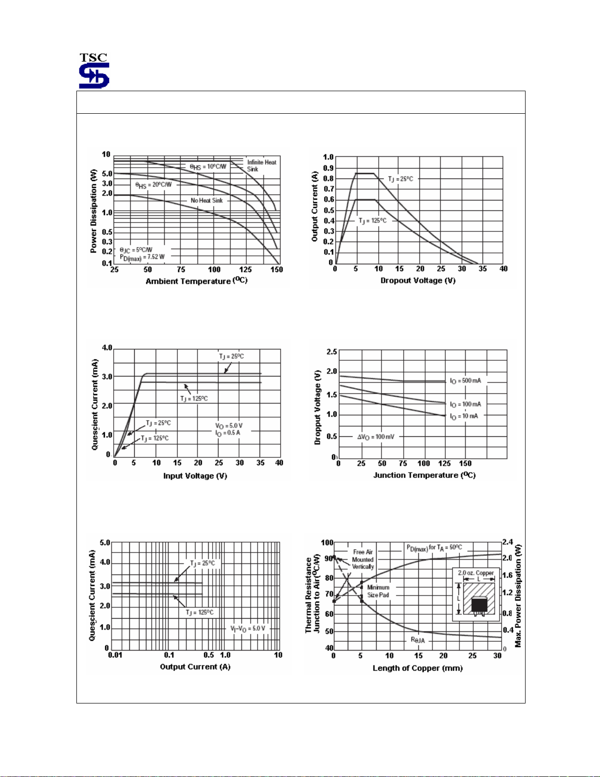
Electrical Characteristics Curve
FIGURE 1 - Worst Case Power Dissipation v.s.
Ambient Temperature
FIGURE 3 – Quiescent Current v.s.
Input Voltage
FIGURE 2 - Peak Output Current v.s.
Dropout Voltage
FIGURE 4 –Dropout Voltage v.s.
Junction Temperature
FIGURE 5 – Quiescent Current v.s.
Output Current
FIGURE 6 – TO-252 Thermal Resistance and
Pd(max) v.s. P.C.B Copper Length
TS79M00 series 6-7 2003/12 rev. A
Page 7
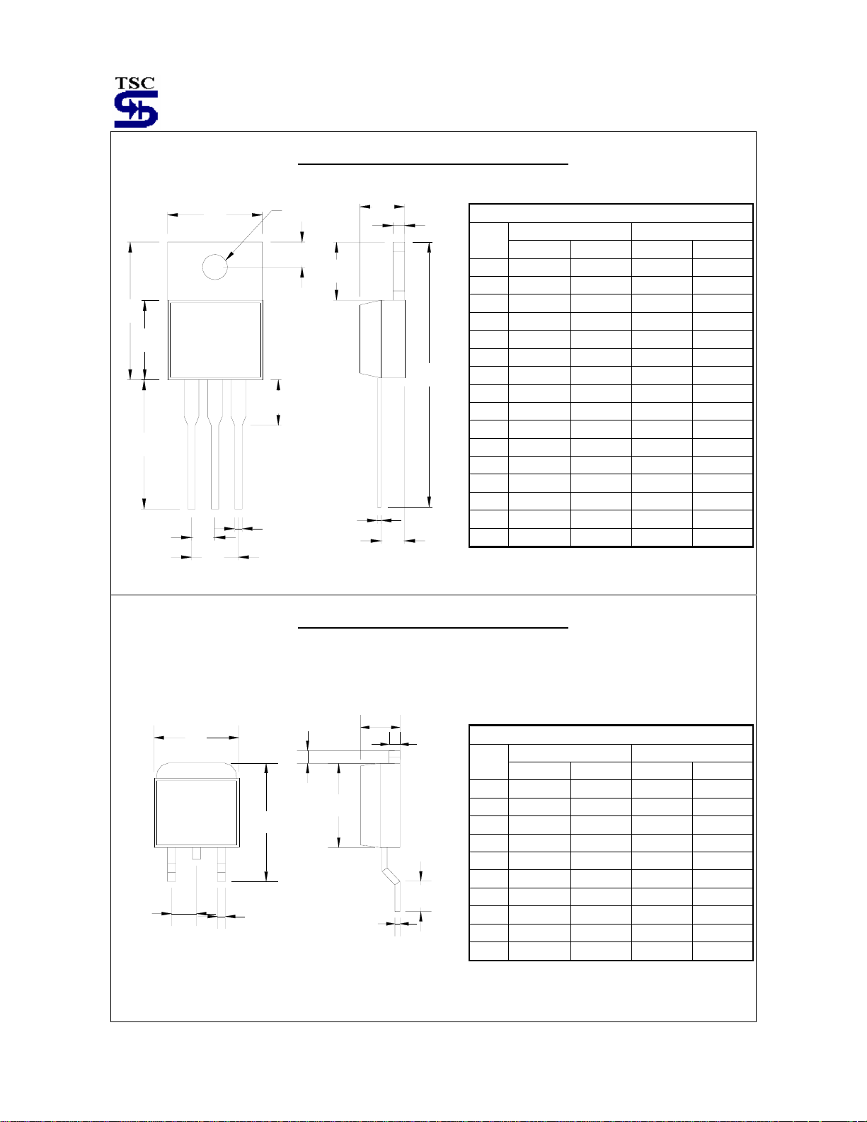
TO-220 Mechanical Drawing
A
B
C
P
J
I
D
H
F
E
G
K
L
DIM
A 10.000 10.500 0.394 0.413
B 3.240 4.440 0.128 0.175
C 2.440 2.940 0.096 0.116
D - 6.350 - 0.250
E 0.381 1.106 0.015 0.040
F 2.345 2.715 0.092 0.058
M
O
N
G 4.690 5.430 0.092 0.107
H 12.700 14.732 0.500 0.581
I 8.382 9.017 0.330 0.355
J 14.224 16.510 0.560 0.650
K 3.556 4.826 0.140 0.190
L 0.508 1.397 0.020 0.055
M 27.700 29.620 1.060 1.230
N 2.032 2.921 0.080 0.115
O 0.255 0.610 0.010 0.024
P 5.842 6.858 0.230 0.270
TO-220 DIMENSION
MILLIMETERS INCHES
MIN MAX MIN MAX
TO-252 Mechanical Drawing
J
A
B
D
C
E
F
DIM
A 6.570 6.840 0.259 0.269
I
G
H
B 9.250 10.400 0.364 0.409
C 0.550 0.700 0.022 0.028
D 2.560 2.670 0.101 0.105
E 2.300 2.390 0.090 0.094
F 0.490 0.570 0.019 0.022
G 1.460 1.580 0.057 0.062
H 0.520 0.570 0.020 0.022
I 5.340 5.550 0.210 0.219
J 1.460 1.640 0.057 0.065
TO-252 DIMENSION
MILLIMETERS INCHES
MIN MAX MIN MAX
TS79M00 series 7-7 2003/12 rev. A
 Loading...