

Page 1

TO-92
SOT
-23 SOP
-8
SOT
-
89
Pin
Definition
:
Pin
Definition
:
Pin
Definition
:
Pin
Definition
:
TS78L00 Series
3-Terminal 100mA Positive Voltage Regulator
1. Output
2. Ground
3. Input
1. Output
2. Input
3. Ground
1. Output 8. Input
2. Ground 7. Ground
3. Ground 6. Ground
4. N/C 5. N/C
TS78L00ACY
1. Output
2. Ground
3. Input
TS78L00CY
1. Input
2. Ground
3. Output
General Description
The TS78L00 Series of positive voltage Regulators are inexpensive, easy-to-use devices suitable for a multitude
of applications that require a regulated supply of up to 100mA. Like their higher power TS7800 and TS78M00
Series cousins, these regulators feature internal current limiting and thermal shutdown making them remarkably
rugged. No external components are required with the TS78L00 devices in many applications.
These devices offer a substantial performance advantage over the traditional zener diode-resistor combination,
as output impedance and quiescent current are substantially reduced.
Features
● Output Voltage Range 3.3 to 24V
● Output current up to 100mA
● No external components required
● Internal thermal overload protection
● Internal short-circuit current limiting
● Output transistor safe-area compensation
● Output voltage offered in 4% tolerance
Ordering Information
Part No. Package
TS78LxxCT B0 TO-92 1Kpcs / Bulk
TS78LxxCT A3 TO-92 2Kpcs/ Ammo
TS78LxxACY RM SOT-89 1Kpcs / 7” Reel
TS78LxxCY RM SOT-89 1Kpcs / 7” Reel
TS78LxxCS RL SOP-8 2.5Kpcs / 13” Reel
TS78LxxCX RF SOT-23 3Kpcs / 7” Reel
Note: Refer to detail ordering information table.
Packing
Standard Application Circuit
A common ground is required between the input and the
output voltages. The input voltage must remain typically
2.0V above the output voltage even during the low point
on the Input ripple voltage.
XX = these two digits of the type number indicate
voltage.
* = Cin is required if regulator is located an appreciable
distance from power supply filter.
** = Co is not needed for stability; however, it does
improve transient response.
Absolute Maximum Rating
(TA = 25oC unless otherwise noted)
Parameter Symbol Limit Unit
TS78L03
DC Input Voltage
TS78L24 40
Power Dissipation PD Internal Limited W
Operating Junction Temperature Range TJ 0 ~ +150
Storage Temperature Range T
1/13
VIN
-65~+150
STG
30
V TS78L05 ~ TS78L18 35
o
o
Version: E13
C
C
Page 2

Temperature Coefficient of
TS78L00 Series
3-Terminal 100mA Positive Voltage Regulator
Thermal Performance
Parameter Symbol Limit Unit
TO-92
Thermal Resistance - Junction to Case
Thermal Resistance - Junction to Ambient
Note: Considering 6 cm2 of copper board heat-sink
SOT-23 120
SOT-89 15
SOP-8 20
TO-92
SOT-23 330
SOT-89 55
SOP-8 55
RӨJC
RӨJA
TS78L03 Electrical Characteristics
(Vin=8.3V, Iout=40mA, 0oC≤Tj≤125oC, Cin=0.33uF, Cout=0.1uF; unless otherwise specified.)
Parameter Symbol Test Condition Min Typ Max Unit
Tj=25oC
Output voltage Vout
Line Regulation REGline Tj=25oC
Load Regulation REGload Tj=25oC
Quiescent Current Iq Iout=0, Tj=25oC -- 3 6
Quiescent Current Change ∆Iq
Output Noise Voltage Vn 10Hz≤f≤100KHz, Tj=25oC -- 40 -- µV
Ripple Rejection Ratio RR f=120Hz, 5.8V≤Vin≤20V 41 49 -- dB
Voltage Drop Vdrop Iout=100mA, Tj=25oC -- 2 -- V
Peak Output Current Io peak Tj=25oC -- 0.15 -- A
Output Voltage
Pulse testing techniques are used to maintain the junction temperature as close to the ambient temperature as
possible, and thermal effects must be taken into account separately.
This specification applies only for DC power dissipation permitted by absolute maximum ratings.
∆Vout/ ∆Tj Iout=5mA, 0oC≤Tj≤150oC -- -0.2 --
5.8V≤Vin≤20V,
5mA≤Iout≤100mA
5.8V≤Vin≤20V
Iout=40mA
5mA≤Iout≤100mA -- 15 60
5mA≤Iout≤40mA -- 5 30
5.8V≤Vin≤20V -- -- 1.5
5mA≤Iout≤40mA -- -- 0.1
3.173
3.142
-- 50 150
--
230
3.3 3.432
3.3 3.465
o
C/W
o
C/W
mV/
V
mV
mA
o
C
2/13
Version: E13
Page 3
Temperature Coefficient of
Temperature Coefficient of
TS78L00 Series
3-Terminal 100mA Positive Voltage Regulator
TS78L05 Electrical Characteristics
(Vin=10V, Iout=40mA, 0oC≤Tj≤125oC, Cin=0.33uF, Cout=0.1uF; unless otherwise specified.)
Parameter Symbol Test Condition Min Typ Max Unit
Tj=25oC
Output voltage Vout
Line Regulation REGline Tj=25oC
Load Regulation REGload Tj=25oC
Quiescent Current Iq Iout=0, Tj=25oC -- 3 6
Quiescent Current Change ∆Iq
Output Noise Voltage Vn 10Hz≤f≤100KHz, Tj=25oC -- 40 -- µV
Ripple Rejection Ratio RR f=120Hz, 7.5V≤Vin≤20V 41 49 -- dB
Voltage Drop Vdrop Iout=100mA, Tj=25oC -- 1.7 -- V
Peak Output Current Io peak Tj=25oC -- 0.15 -- A
7.5V≤Vin≤20V,
5mA≤Iout≤100mA
7.5V≤Vin≤20V
Iout=100mA
5mA≤Iout≤100mA -- 20 60
5mA≤Iout≤40mA -- 10 30
7.5V≤Vin≤20V -- -- 1.5
5mA≤Iout≤40mA -- -- 0.1
4.80 5 5.20
4.75 5 5.25
-- 50 150
mV
mA
V
Output Voltage
∆Vout/ ∆Tj Iout=5mA, 0oC≤Tj≤150oC -- -0.65
-- mV/oC
TS78L06 Electrical Characteristics
Vin=12V, Iout=40mA, 0oC≤Tj≤125oC, Cin=0.33uF, Cout=0.1uF; unless otherwise specified.)
Parameter Symbol Test Condition Min Typ Max Unit
Tj=25oC
Output voltage Vout
Line Regulation REGline Tj=25oC
Load Regulation REGload Tj=25oC
Quiescent Current Iq Iout=0, Tj=25oC -- 3 6
Quiescent Current Change ∆Iq
Output Noise Voltage Vn 10Hz≤f≤100KHz, Tj=25oC -- 40 -- µV
Ripple Rejection Ratio RR f=120Hz, 8.5V≤Vin≤21V 41 49 -- dB
Voltage Drop Vdrop Iout=100mA, Tj=25oC -- 1.7 -- V
Peak Output Current Io peak Tj=25oC -- 0.15 -- A
Output Voltage
Pulse testing techniques are used to maintain the junction temperature as close to the ambient temperature as
possible, and thermal effects must be taken into account separately.
This specification applies only for DC power dissipation permitted by absolute maximum ratings.
∆Vout/ ∆Tj Iout= 5mA, 0oC≤Tj≤150oC -- -0.75
8.5V≤Vin≤21V,
5mA≤Iout≤100mA
8.5V≤Vin≤21V
Iout=40mA
5mA≤Iout≤100mA -- 12 60
5mA≤Iout≤40mA -- 4 30
8.5V≤Vin≤21V -- -- 1.5
5mA≤Iout≤40mA -- -- 0.1
5.76 6 6.24
5.70 6 6.30
-- 50 150
-- mV/oC
V
mV
mA
3/13
Version: E13
Page 4

Temperature Coefficient of
Temperature Coefficient of
TS78L00 Series
3-Terminal 100mA Positive Voltage Regulator
TS78L08 Electrical Characteristics
Vin=14V, Iout=40mA, 0oC≤Tj≤125oC, Cin=0.33uF, Cout=0.1uF; unless otherwise specified.)
Parameter Symbol Test Condition Min Typ Max Unit
Tj=25oC
Output voltage Vout
Line Regulation REGline Tj=25oC
Load Regulation REGload Tj=25oC
Quiescent Current Iq Iout=0, Tj=25oC -- 3 6
Quiescent Current Change ∆Iq
Output Noise Voltage Vn 10Hz≤f≤100KHz, Tj=25oC -- 60 -- µV
Ripple Rejection Ratio RR f=120Hz, 10.5V≤Vin≤23V 37 57 -- dB
Voltage Drop Vdrop Iout=100mA, Tj=25oC -- 1.7 -- V
Peak Output Current Io peak Tj=25oC -- 0.15 -- A
10.5V≤Vin≤23V,
5mA≤Iout≤100mA
10.5V≤Vin≤23V
Iout=40mA
5mA≤Iout≤100mA -- 25 80
5mA≤Iout≤40mA -- 10 40
10.5V≤Vin≤23V -- -- 1.5
5mA≤Iout≤40mA -- -- 0.1
7.69 8 8.32
7.61 8 8.40
-- 80 160
mV
mA
V
Output Voltage
∆Vout/ ∆Tj Iout=5mA, 0oC≤Tj≤150oC -- -0.8 -- mV/oC
TS78L09 Electrical Characteristics
Vin=15V, Iout=40mA, 0oC≤Tj≤125oC, Cin=0.33uF, Cout=0.1uF; unless otherwise specified.)
Parameter Symbol Test Condition Min Typ Max Unit
Tj=25oC
Output voltage Vout
Line Regulation REGline Tj=25oC
Load Regulation REGload Tj=25oC
Quiescent Current Iq Iout=0, Tj=25oC -- 3 6
Quiescent Current Change ∆Iq
Output Noise Voltage Vn 10Hz≤f≤100KHz, Tj=25oC -- 60 -- µV
Ripple Rejection Ratio RR f=120Hz, 11.5V≤Vin≤23V 37 57 -- dB
Voltage Drop Vdrop Iout=100mA, Tj=25oC -- 1.7 -- V
Peak Output Current Io peak Tj=25oC -- 0.15 -- A
Output Voltage
Pulse testing techniques are used to maintain the junction temperature as close to the ambient temperature as
possible, and thermal effects must be taken into account separately.
This specification applies only for DC power dissipation permitted by absolute maximum ratings.
∆Vout/ ∆Tj Iout=5mA, 0oC≤Tj≤150oC -- -0.9 -- mV/oC
11.5V≤Vin≤23V,
5mA≤Iout≤100mA
11.5V≤Vin≤23V
Iout=40mA
5mA≤Iout≤100mA -- 30 90
5mA≤Iout≤40mA -- 15 45
11.5V≤Vin≤23V -- -- 1.5
5mA≤Iout≤40mA -- -- 0.1
8.65 9 9.36
8.57 9 9.45
-- 90 180
V
mV
mA
4/13
Version: E13
Page 5

Temperature Coefficient of
Temperature Coefficient of
TS78L00 Series
3-Terminal 100mA Positive Voltage Regulator
TS78L12 Electrical Characteristics
Vin=19V, Iout=40mA, 0oC ≤Tj≤125oC, Cin=0.33uF, Cout=0.1uF; unless otherwise specified.)
Parameter Symbol Test Condition Min Typ Max Unit
Tj=25oC
Output voltage Vout
Line Regulation REGline Tj=25oC
Load Regulation REGload Tj=25oC
Quiescent Current Iq Iout=0, Tj=25oC -- 3 6.5
Quiescent Current Change ∆Iq
Output Noise Voltage Vn 10Hz≤f≤100KHz, Tj=25oC -- 80 -- µV
Ripple Rejection Ratio RR f=120Hz, 14.5V≤Vin≤27V 37 42 -- dB
Voltage Drop Vdrop Iout=100mA, Tj=25oC -- 1.7 -- V
Peak Output Current Io peak Tj=25oC -- 0.15 -- A
14.5V≤Vin≤27V,
5mA≤Iout≤100mA
14.5V≤Vin≤27V
Iout=40mA
5mA≤Iout≤100mA -- 40 120
5mA≤Iout≤40mA -- 20 60
14.5V≤Vin≤27V -- -- 1.5
5mA≤Iout≤40mA -- -- 0.1
11.53
11.42
-- 120 240
12 12.48
12 12.60
mV
mA
V
Output Voltage
∆Vout/ ∆Tj Iout=5mA, 0oC≤Tj≤150oC -- -1.0 -- mV/oC
TS78L15 Electrical Characteristics
Vin=23V, Iout=40mA, 0oC≤Tj≤125oC, Cin=0.33uF, Cout=0.1uF; unless otherwise specified.)
Parameter Symbol Test Condition Min Typ Max Unit
Tj=25oC
Output voltage Vout
Line Regulation REGline Tj=25oC
Load Regulation REGload Tj=25oC
Quiescent Current Iq Iout=0, Tj=25oC -- 3 6.6
Quiescent Current Change ∆Iq
Output Noise Voltage Vn 10Hz≤f≤100KHz, Tj=25oC -- 90 -- µV
Ripple Rejection Ratio RR f=120Hz, 17.5V≤Vin≤30V 34 39 -- dB
Voltage Drop Vdrop Iout=100mA, Tj=25oC -- 1.7 -- V
Peak Output Current Io peak Tj=25oC -- 0.15 -- A
Output Voltage
Pulse testing techniques are used to maintain the junction temperature as close to the ambient temperature as
possible, and thermal effects must be taken into account separately.
This specification applies only for DC power dissipation permitted by absolute maximum ratings.
∆Vout/ ∆Tj Iout=5mA, 0oC≤Tj≤150oC -- -1.3 --
17.5V≤Vin≤30V,
5mA≤Iout≤100mA
17.5V≤Vin≤30V
Iout=40mA
5mA≤Iout≤100mA -- 50 150
5mA≤Iout≤40mA -- 25 75
17.5V≤Vin≤30V -- -- 1.5
5mA≤Iout≤40mA -- -- 0.1
14.42
14.28
-- 150 300
15 15.60
15 15.75
V
mV
mA
mV/
o
C
5/13
Version: E13
Page 6
Temperature Coefficient of
Temperature Coefficient of
TS78L00 Series
3-Terminal 100mA Positive Voltage Regulator
TS78L18 Electrical Characteristics
Vin=27V, Iout=40mA, 0oC≤Tj≤125oC, Cin=0.33uF, Cout=0.1uF; unless otherwise specified.)
Parameter Symbol Test Condition Min Typ Max Unit
Tj=25oC
Output voltage Vout
Line Regulation REGline Tj=25oC
Load Regulation REGload Tj=25oC
Quiescent Current Iq Iout=0, Tj=25oC -- 3 6.5
Quiescent Current Change ∆Iq
Output Noise Voltage Vn 10Hz≤f≤100KHz, Tj=25oC -- 150 -- µV
Ripple Rejection Ratio RR f=120Hz, 21V≤Vin≤33V 33 48 -- dB
Voltage Drop Vdrop Iout=100mA, Tj=25oC -- 1.7 -- V
Peak Output Current Io peak Tj=25oC -- 0.15 -- A
21V≤Vin≤33V,
5mA≤Iout≤100mA
21≤Vin≤33V
Iout=40mA
5mA≤Iout≤100mA -- 60 180
5mA≤Iout≤40mA -- 30 90
21V≤Vin≤33V -- -- 1.5
5mA≤Iout≤40mA -- -- 0.1
17.30
17.14
-- 180 360
18 18.72
18 18.90
mV
mA
V
Output Voltage
∆Vout/ ∆Tj Iout=5mA, 0oC≤Tj≤150oC -- -1.5 -- mV/oC
TS78L24 Electrical Characteristics
Vin=33V, Iout=40mA, 0oC≤Tj≤125oC, Cin=0.33uF, Cout=0.1uF; unless otherwise specified.)
Parameter Symbol Test Condition Min Typ Max Unit
Tj=25oC
Output voltage Vout
Line Regulation REGline Tj=25oC
Load Regulation REGload Tj=25oC
Quiescent Current Iq Iout=0, Tj=25oC -- 4 7
Quiescent Current Change ∆Iq
Output Noise Voltage Vn 10Hz≤f≤100KHz, Tj=25oC -- 200 -- µV
Ripple Rejection Ratio RR f=120Hz, 27V≤Vin≤38V 31 45 -- dB
Voltage Drop Vdrop Iout=100mA, Tj=25oC -- 1.7 -- V
Peak Output Current Io peak Tj=25oC -- 0.15 -- A
Output Voltage
Pulse testing techniques are used to maintain the junction temperature as close to the ambient temperature as
possible, and thermal effects must be taken into account separately.
This specification applies only for DC power dissipation permitted by absolute maximum ratings.
∆Vout/ ∆Tj Iout=5mA, 0oC≤Tj≤150oC -- -2.0 -- mV/oC
27V≤Vin≤38V,
5mA≤Iout≤100mA
27≤Vin≤38V
Iout=40mA
5mA≤Iout≤100mA -- 80 240
5mA≤Iout≤40mA -- 40 120
27V≤Vin≤38V -- -- 1.5
5mA≤Iout≤40mA -- -- 0.1
23.07
22.85
-- 200 400
24 24.96
24 25.20
V
mV
mA
6/13
Version: E13
Page 7

be a 50Ω. 1/2W resistor and the output voltage compliance
TS78L00 Series
3-Terminal 100mA Positive Voltage Regulator
Application Information
Design Considerations
The TS78L00 Series of fixed voltage regulators are designed with Thermal Overload Protection that shuts down
the circuit when subjected to an excessive power overload condition. Internal Short Circuit protection Limits the
maximum current the circuit will pass.
In many low current applications, compensation capacitors are not required. However, it is recommended that the
regulator input be bypassed with a capacitor if the regulator is connected to the power supply filter with long wire
lengths, or if the output load capacitance is large. The input bypass capacitor should be selected to provide good
high-frequency characteristics to insure stable operation under all load conditions. A 0.33uF or larger tantalum,
mylar, or other capacitor having low internal impedance at high frequencies should be chosen. The bypass
capacitor should be mounted with the shortest possible leads directly across the regulators input terminals. Good
construction techniques should be used to minimize ground loops and lead resistance drops since the regulator
has no external sense lead. Bypassing the output is also recommended.
FIGURE 1 – Current Regulator
The TS78L00 regulators can also be used as a current
source when connected as above. In order to minimize
dissipation the TS78L05 is chosen in this application.
Resistor R determines the current as follows:
IIB=3.8mA over lined and load changes
For example, a 100mA current source would require R to
FIGURE 2 – ±±±±15V Tracking Voltage Regulator
FIGURE 3 – ±±±±15V Tracking Voltage Regulator
would be the input voltage less 7V.
7/13
Version: E13
Page 8
Packing code information
TS78L00 Series
3-Terminal 100mA Positive Voltage Regulator
Ordering information
Voltage TO-92 SOT-89 SOP-8 SOT-23
3.3V
5V
6V
8V
9V
12V
15V
18V
24V
Packing
TS78L03CT B0
TS78L03CT A3
TS78L05CT B0
TS78L05CT A3
TS78L06CT B0
TS78L06CT A3
TS78L08CT B0
TS78L08CT A3
TS78L09CT B0
TS78L09CT A3
TS78L12CT B0
TS78L12CT A3
TS78L15CT B0
TS78L15CT A3
TS78L18CT B0
TS78L18CT A3
TS78L24CT B0
TS78L24CT A3
B0: 1Kpcs / Bulk
A3: 2Kpcs / Ammo
TS78L03ACY RM
TS78L03CY RM
TS78L05ACY RM
TS78L05CY RM
TS78L06ACY RM
TS78L06CY RM
TS78L08ACY RM
TS78L08CY RM
TS78L09ACY RM
TS78L09CY RM
TS78L12ACY RM
TS78L12CY RM
TS78L15ACY RM
TS78L15CY RM
TS78L18ACY RM
TS78L18CY RM
TS78L24ACY RM
TS78L24CY RM
1Kpcs / 7" Reel 2.5Kpcs / 13" Reel 3Kpcs / 7"Reel
TS78L03CS RL TS78L03CX RF
TS78L05CS RL TS78L05CX RF
TS78L08CS RL TS78L08CX RF
TS78L09CS RL TS78L09CX RF
TS78L12CS RL TS78L12CX RF
TS78L15CS RL TS78L15CX RF
TS78L18CS RL TS78L18CX RF
TS78L24CS RL TS78L24CX RF
8/13
Version: E13
Page 9

= Output Voltage
= Year Code
= Month Code
= Lot Code
TS78L00 Series
3-Terminal 100mA Positive Voltage Regulator
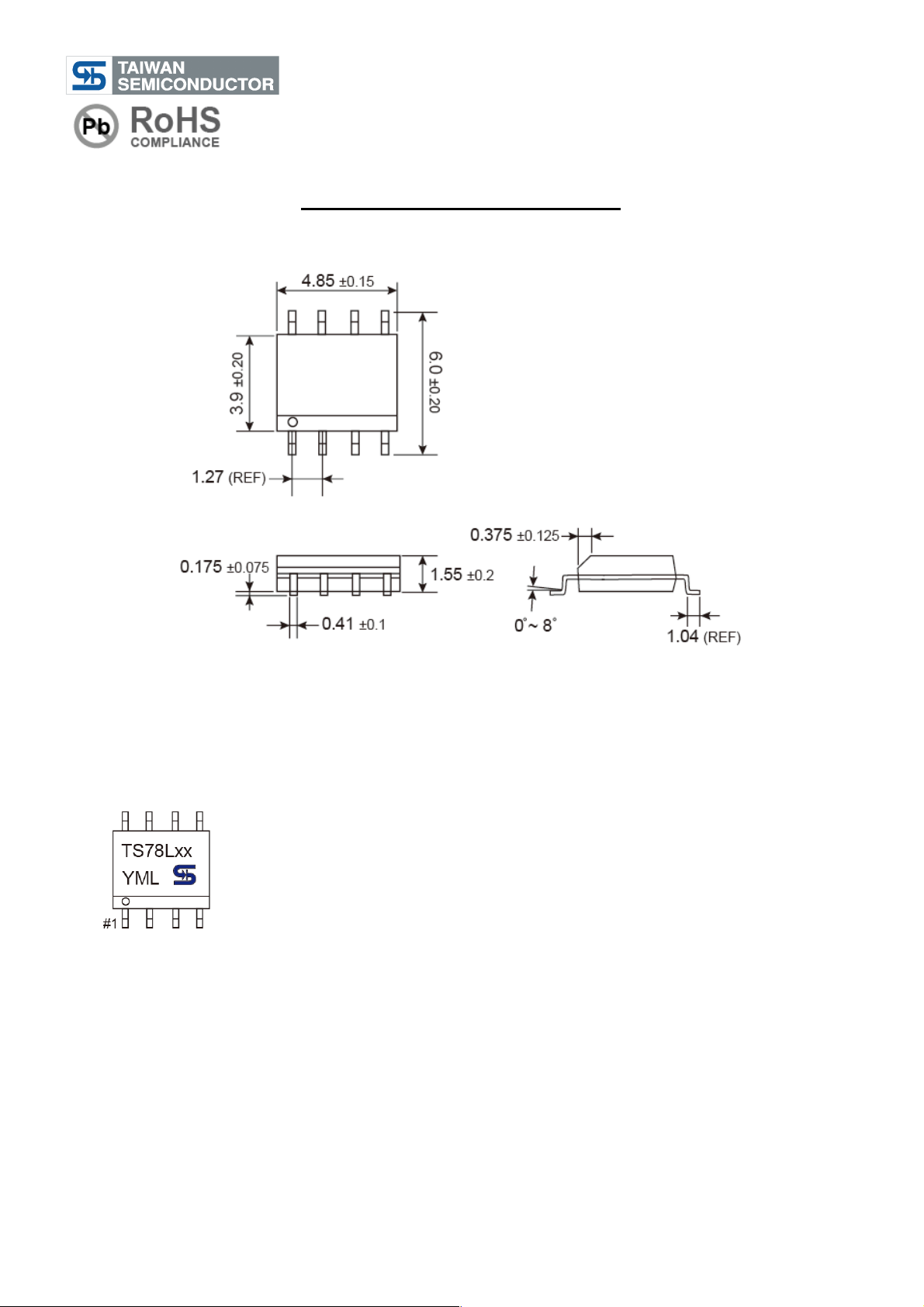
TO-92 Mechanical Drawing
Marking Diagram
XX
Y
M
L
Unit: Millimeters
(03=3.3V, 05=5V, 06=6V, 08=8V, 09=9V, 12=12V, 15=15V, 18=18V, 24=24V)
(A=Jan, B=Feb, C=Mar, D=Apl, E=May, F=Jun, G=Jul, H=Aug, I=Sep,
J=Oct, K=Nov, L=Dec)
9/13
Version: E13
Page 10

= Output Voltage
= Year Code
= Month Code
= Lot Code
= Output Voltage
= Year Code
= Month Code
= Lot Code
= TS78LxxACY
TS78L00 Series
3-Terminal 100mA Positive Voltage Regulator
SOT-89 Mechanical Drawing
Marking Diagram
X
X
(03=3.3V, 05=5V, 06=6V, 08=8V, 09=9V, 12=12V, 15=15V, 18=18V, 24=24V)
Y
M
(A=Jan, B=Feb, C=Mar, D=Apl, E=May, F=Jun, G=Jul, H=Aug, I=Sep,
J=Oct, K=Nov, L=Dec)
L
XX
(03=3.3V, 05=5V, 06=6V, 08=8V, 09=9V, 12=12V, 15=15V, 18=18V, 24=24V)
Y
M
(A=Jan, B=Feb, C=Mar, D=Apl, E=May, F=Jun, G=Jul, H=Aug, I=Sep,
J=Oct, K=Nov, L=Dec)
L
A
Unit: Millimeters
10/13
Version: E13
Page 11
= Output Voltage
= Year Code
= Month Code
= Lot Code
TS78L00 Series
3-Terminal 100mA Positive Voltage Regulator
SOP-8 Mechanical Drawing
Marking Diagram
XX
Y
M
L
Unit: Millimeters
(03=3.3V, 05=5V, 08=8V, 09=9V, 12=12V, 15=15V, 18=18V, 24=24V)
(A=Jan, B=Feb, C=Mar, D=Apl, E=May, F=Jun, G=Jul, H=Aug, I=Sep,
J=Oct, K=Nov, L=Dec)
11/13
Version: E13
Page 12
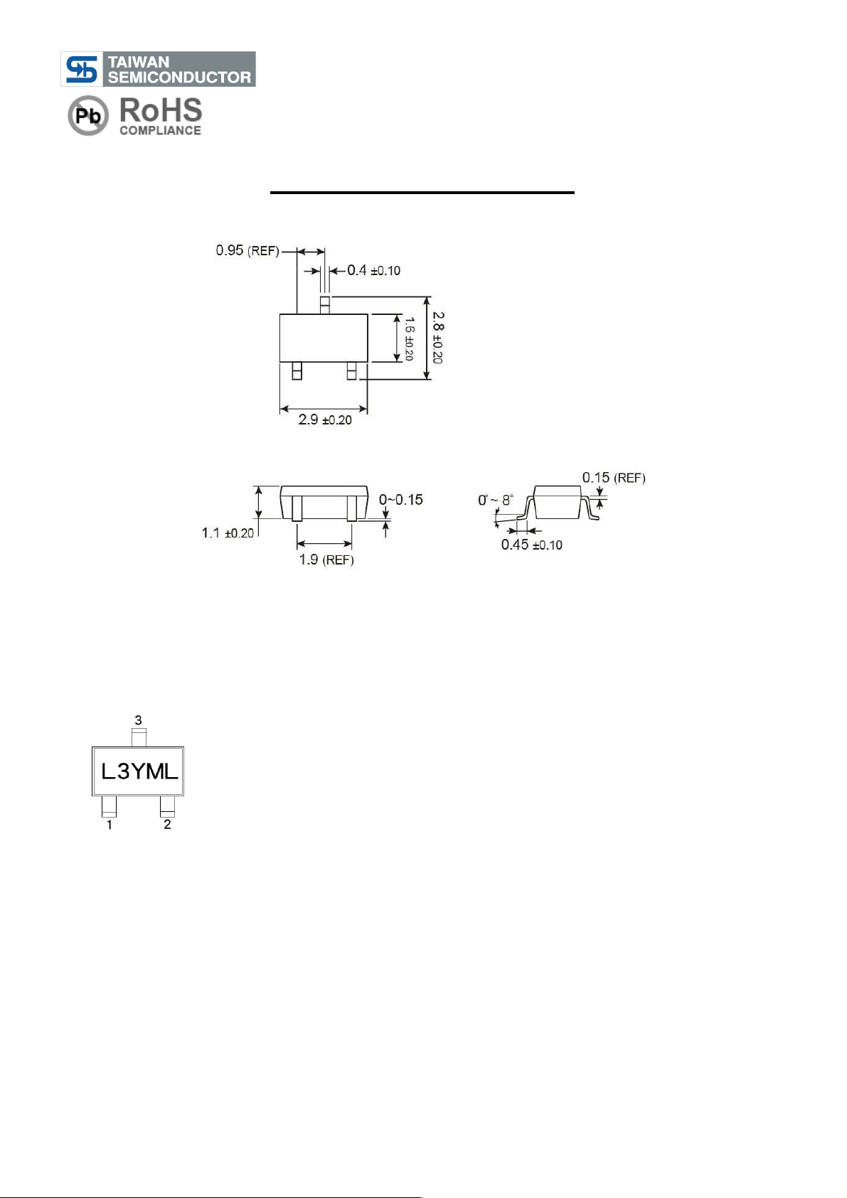
= Device Voltage Code
= Year Code
= Month Code
= Lot Code
TS78L00 Series
3-Terminal 100mA Positive Voltage Regulator
SOT-23 Mechanical Drawing
Marking Diagram
L
3
(L3=3.3V, L5=5V, L8=8V, L9=9V, L2=12V, A=15V, D=18V, J=24V)
Y
M
(A=Jan, B=Feb, C=Mar, D=Apl, E=May, F=Jun, G=Jul, H=Aug, I=Sep,
J=Oct, K=Nov, L=Dec)
L
Unit: Millimeters
12/13
Version: E13
Page 13

TS78L00 Series
3-Terminal 100mA Positive Voltage Regulator
Notice
Specifications of the products displayed herein are subject to change without notice. TSC or anyone on its behalf,
assumes no responsibility or liability for any errors or inaccuracies.
Information contained herein is intended to provide a product description only. No license, express or implied, to
any intellectual property rights is granted by this document. Except as provided in TSC’s terms and conditions of
sale for such products, TSC assumes no liability whatsoever, and disclaims any express or implied warranty,
relating to sale and/or use of TSC products including liability or warranties relating to fitness for a particular purpose,
merchantability, or infringement of any patent, copyright, or other intellectual property right.
The products shown herein are not designed for use in medical, life-saving, or life-sustaining applications.
Customers using or selling these products for use in such applications do so at their own risk and agree to fully
indemnify TSC for any damages resulting from such improper use or sale.
13/13
Version: E13
 Loading...