

Page 1
TLC556, TLC556Y
DUAL LinCMOS TIMERS
SLFS047B – FEBRUARY 1984 – REVISED SEPTEMBER 1997
D
Very Low Power Consumption ...2 mW
Typ at VDD = 5 V
D
Capable of Operation in Astable Mode
D
CMOS Output Capable of Swinging Rail to
Rail
D
High Output-Current Capability
Sink 100 mA Typ
Source 10 mA Typ
D
Output Fully Compatible With CMOS, TTL,
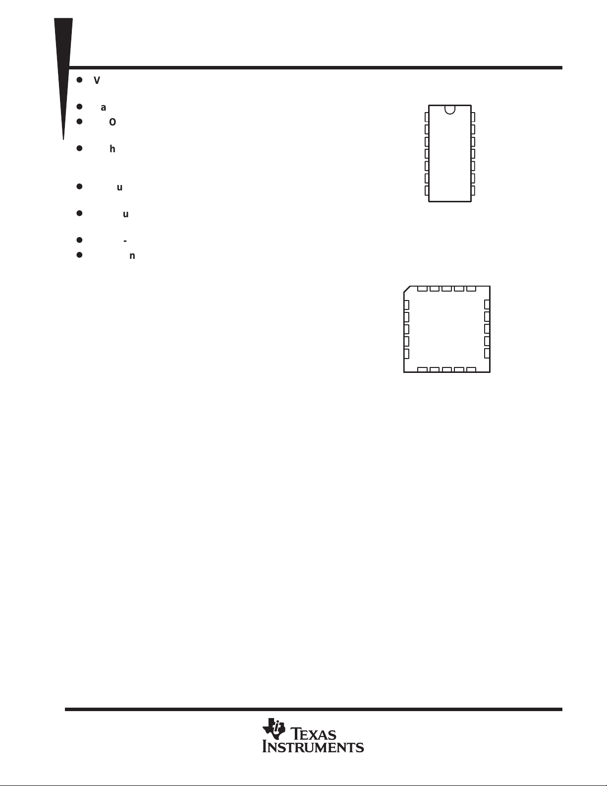
D, J, OR N PACKAGE
(TOP VIEW)
1 DISCH
1 THRES
1 CONT
1 RESET
1 OUT
1 TRIG
GND
1
2
3
4
5
6
7
13
12
11
10
9
8
DD
2 DISCH
2 THRES
2 CONT
2 RESET
2 OUT
2 TRIG
V
14
and MOS
D
Low Supply Current Reduces Spikes
During Output Transitions
D
Single-Supply Operation From 2 V to 15 V
D
Functionally interchangeable With the
NE556; Has Same Pinout
description
The TLC556 series are monolithic timing circuits
fabricated using the TI LinCMOS process, which
provides full compatibility with CMOS, TTL, and
MOS logic and operates at frequencies up to
2 MHz. Accurate time delays and oscillations are
1 CONT
NC
1 RESET
NC
1 OUT
FK PACKAGE
(TOP VIEW)
1 THRES
1 DISCH
NC
3 2 1 20 19
4
5
6
7
8
910111213
DD
V
2 DISCH
18
17
16
15
14
2 THRES
NC
2 CONT
NC
2 RESET
possible with smaller, less-expensive timing
capacitors than the NE556 because of the high
input impedance. Power consumption is low
across the full range of power supply voltages.
Like the NE556, the TLC556 has a trigger level
NC–No internal connection
GND
1 TRIG
NC
2 OUT
2 TRIG
approximately one-third of the supply voltage and
a threshold level approximately two-thirds of the supply voltage. These levels can be altered by use of the control
voltage terminal. When the trigger input falls below the trigger level, the flip-flop is set and the output goes high.
If the trigger input is above the trigger level and the threshold input is above the threshold level, the flip-flop is
reset and the output is low. The reset input can override all other inputs and can be used to initiate a new timing
cycle. If the reset input is low, the flip-flop is reset and the output is low. Whenever the output is low, a
low-impedance path is provided between the discharge terminal and ground.
While the CMOS output is capable of sinking over 100 mA and sourcing over 10 mA, the TLC556 exhibits greatly
reduced supply-current spikes during output transitions. This minimizes the need for the large decoupling
capacitors required by the NE556.
These devices have internal electrostatic-discharge (ESD) protection circuits that prevent catastrophic failures
at voltages up to 2000 V as tested under MIL-STD-883C, Method 3015. However, care should be exercised in
handling these devices, as exposure to ESD may result in degradation of the device parametric performance.
All unused inputs should be tied to an appropriate logic level to prevent false triggering.
The TLC556C is characterized for operation from 0°C to 70°C. The TLC556I is characterized for operation from
–40°C to 85°C. The TLC556M is characterized for operation over the full military temperature range of –55°C
to 125°C.
LinCMOS is a trademark of Texas Instruments Incorporated.
PRODUCTION DATA information is current as of publication date.
Products conform to specifications per the terms of Texas Instruments
standard warranty. Production processing does not necessarily include
testing of all parameters.
POST OFFICE BOX 655303 • DALLAS, TEXAS 75265
Copyright 1997, Texas Instruments Incorporated
1
Page 2
TLC556, TLC556Y
T
V
CHIP FORM
DUAL LinCMOS TIMERS
SLFS047B – FEBRUARY 1984 – REVISED SEPTEMBER 1997
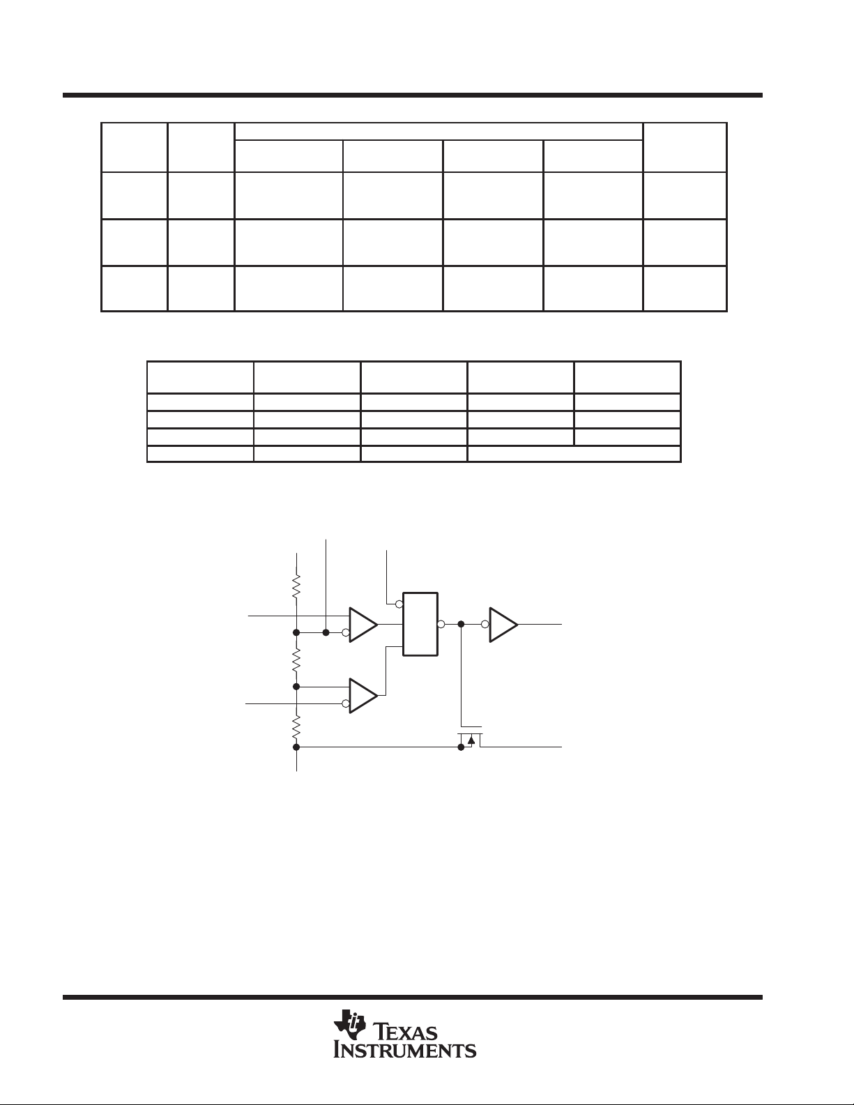
AVAILABLE OPTIONS
A
RANGE
O°C
to
70°C
–4O°C
to
85°C
–55°C
to
125°C
The D package is available taped and reeled. Add the suffix R to the device type (e.g., TLC556CDR).
†
DD
RANGE
2 V
to
18 V
3 V
to
18 V
5 V
to
18 V
RESET
VOLTAGE
< MIN Irrelevant Irrelevant L On
> MAX < MIN Irrelevant H Off
>MAX >MAX >MAX L On
> MAX > MAX < MIN As previously established
For conditions shown as MIN or MAX, use the appropriate value specified under electrical characteristics.
SMALL OUTLINE
(D)
TLC556CD TLC556CN TLC556Y
TLC556lD TLC556IN
TLC556MD TLC556MFK TLC556MJ TLC556MN
†
TRIGGER
VOLTAGE
CHIP CARRIER
FUNCTION TABLE
†
PACKAGE
(FK)
THRESHOLD
VOLTAGE
†
CERAMIC DIP
(J)
OUTPUT
PLASTIC DIP
(N)
DISCHARGE
SWITCH
(Y)
functional block diagram (each timer)
CONT
V
DD
14
R
THRES
TRIG
RESET can override TRIG and THRES.
TRIG can override THRES.
Pin numbers shown are for the D, J, or N packages.
2
R
6
R
7
GND
RESET
3
4
R1
RS1
5
OUT
1
DISCH
2
POST OFFICE BOX 655303 • DALLAS, TEXAS 75265
Page 3
TLC556, TLC556Y
DUAL LinCMOS TIMERS
SLFS047B – FEBRUARY 1984 – REVISED SEPTEMBER 1997
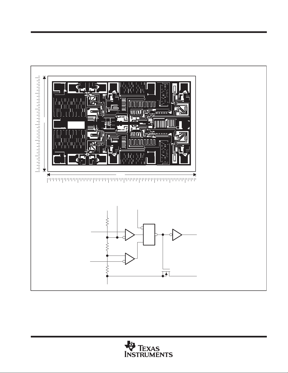
TLC556Y chip information
These chips, properly assembled, display characteristics similar to the TLC556 (see electrical table). Thermal
compression or ultrasonic bonding may be used on the doped aluminum bonding pads. Chips may be mounted
with conductive epoxy or a gold-silicon preform.
BONDING PAD ASSIGNMENTS
CHIP THICKNESS: 15 TYPICAL
BONDING PADS: 4 × 4 MINIMUM
TJ max = 150°C
61
TOLERANCES ARE ±10%
ALL DIMENSIONS ARE IN MILS
NO BACKSIDE METALLIZATION
PIN (7) INTERNALLY CONNECTED
TO BACKSIDE OF CHIP
THRESH
TRIG
97
FUNCTIONAL BLOCK DIAGRAM (EACH TIMER)
(2)
(6)
(14)
V
DD
GND
CONT
R
R
R
(7)
(3)
RESET
(4)
R1
RS1
(5)
(1)
OUT
DISCH
POST OFFICE BOX 655303 • DALLAS, TEXAS 75265
3
Page 4
TLC556, TLC556Y
DUAL LinCMOS TIMERS
SLFS047B – FEBRUARY 1984 – REVISED SEPTEMBER 1997
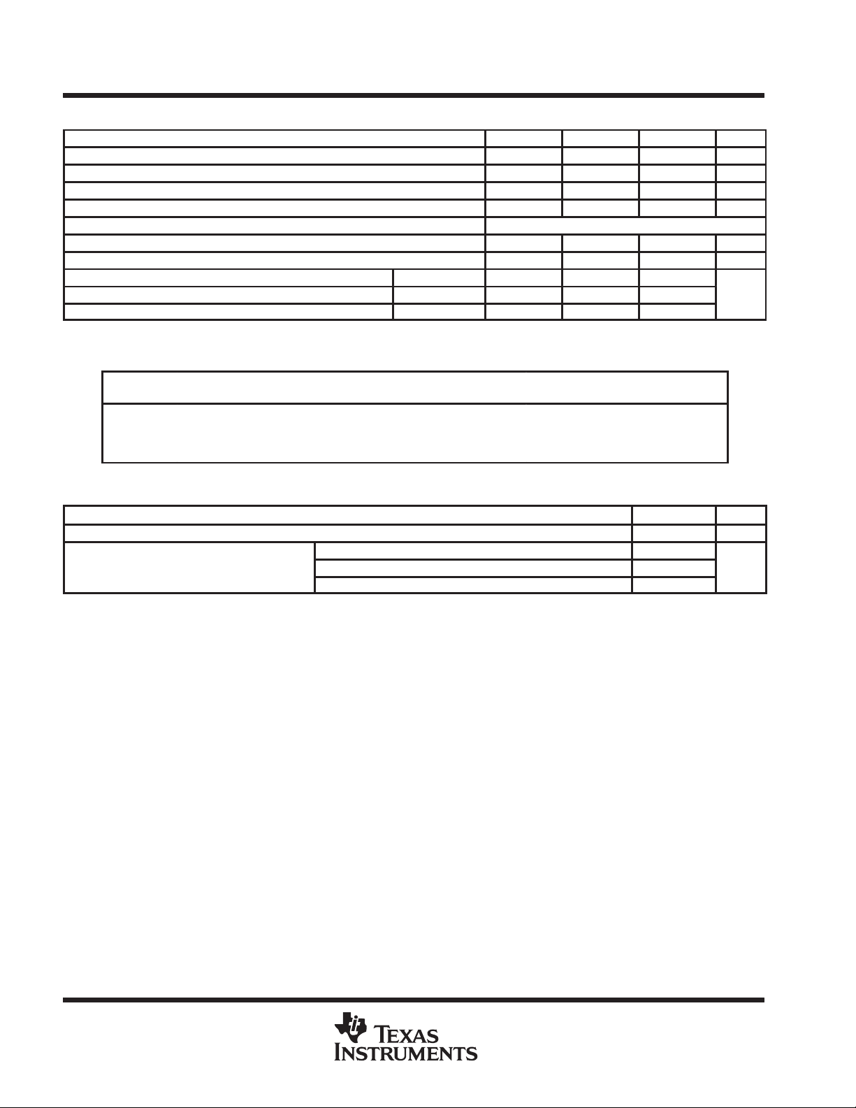
absolute maximum ratings over operating free-air temperature (unless otherwise noted)
TLC556C TLC556I TLC556M UNIT
Supply voltage, VDD (see Note 1) 18 18 18 V
Input voltage range, V
Sink current, discharge or output 150 150 150 mA
Source current, output 15 15 15 mA
Continuous total power dissipation See Dissipation Rating Table
Operating free-air temperature range 0 to 70 –40 to 85 –55 to 125 °C
Storage temperature range –65 to 150 –65 to 150 –65 to 150 °C
Case temperature for 60 seconds FK package 260
Lead temperature 1,6 mm (1/16 inch) from case for 60 seconds J package 300
Lead temperature 1,6 mm (1/16 inch) from case for 10 seconds D or N package 260 260
NOTE 1: All voltage values are with respect to network ground terminal.
PACKAGE
D
FK
N
I
DISSIPATION RATING TABLE
TA ≤ 25°C
POWER RATING
950 mW
J
1375 mW
1375 mW
1150 mW
DERATING FACTOR
ABOVE TA = 25°C
7.6 mW/°C
11.0 mW/°C
11.0 mW/°C
9.2 mW/°C
TA = 70°C
POWER RATING
608 mW
880 mW
880 mW
736 mW
–0.3 to V
–0.3 to V
DD
TA = 85°C
POWER RATING
494 mW
715 mW
715 mW
598 mW
–0.3 to V
DD
TA = 125°C
POWER RATING
N/A
275 mW
275 mW
N/A
DD
V
°C
recommended operating conditions
Supply voltage, V
Operating free-air temperature range, T
DD
A
MIN MAX UNIT
2 15 V
TLC556C 0 70
TLC556I –40 85 °C
TLC556M –55 125
4
POST OFFICE BOX 655303 • DALLAS, TEXAS 75265
Page 5
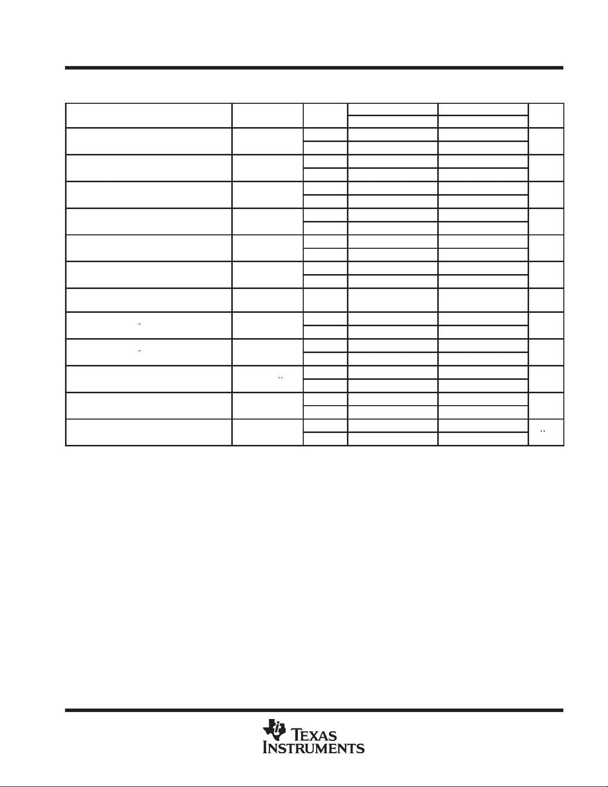
PARAMETER
T
†
UNIT
VITInput threshold voltage
V
Threshold current
pA
V
Trigger voltage
V
I
Trigger current
pA
V
Reset voltage
V
I
Reset current
pA
g
I
mA
V
g
nA
VOHHigh-level output voltage
I
300 µA
V
VOLLow-level output voltage
I
mA
V
IDDSupply current
See Note 2
A
TLC556, TLC556Y
DUAL LinCMOS TIMERS
SLFS047B – FEBRUARY 1984 – REVISED SEPTEMBER 1997
electrical characteristics at specified free-air temperature, VDD = 2 V for TLC556C, VDD = 3 V for
TLC556I
TEST
CONDITIONS
p
(trigger)
(trigger)
(reset)
(reset)
Control voltage (open circuit) as
a percentage of supply voltage
Discharge switch on-state voltage
Discharge switch off-state current
p
p
pp
†
Full range is 0°C to 70°C for TLC556C and –40°C to 85°C for TLC556I.
NOTE 2: These values apply for the expected operating configurations in which THRES is connected directly to DISCH or TRIG.
OL
OH
OL
= 1
= –
= 1
A
25°C 0.95 1.33 1.65 1.6 2 2.4
Full range 0.85 1.75 1.5 2.5
25°C 10 10
MAX 75 150
25°C 0.4 0.67 0.95 0.71 1 1.29
Full range 0.3 1.05 0.61 1.39
25°C 10 10
MAX 75 150
25°C 0.4 1.1 1.5 0.4 1.1 1.5
Full range 0.3 1.8 0.3 1.8
25°C 10 10
MAX 75 150
MAX 66.7% 66.7%
25°C 0.04 0.2 0.03 0.2
Full range 0.25 0.375
25°C 0.1 0.1
MAX 0.5 120
25°C 1.5 1.9 1.5 1.9
Full range 1.5 2.5
25°C 0.07 0.3 0.07 0.3
Full range 0.35 0.4
25°C 130 500 130 500
Full range 800 1000
TLC556C TLC556I
MIN TYP MAX MIN TYP MAX
p
p
p
µ
POST OFFICE BOX 655303 • DALLAS, TEXAS 75265
5
Page 6
TLC556, TLC556Y
PARAMETER
T
†
UNIT
V
V
Th
t
A
V
Tri
V
I
Tri
t
A
V
R
V
I
R
t
A
g
I
10 mA
V
g
A
V
g
I
1 mA
V
I
8 mA
V
I
5 mA
V
I
3.2 mA
IDDSupply current
See Note 2
µA
DUAL LinCMOS TIMERS
SLFS047B – FEBRUARY 1984 – REVISED SEPTEMBER 1997
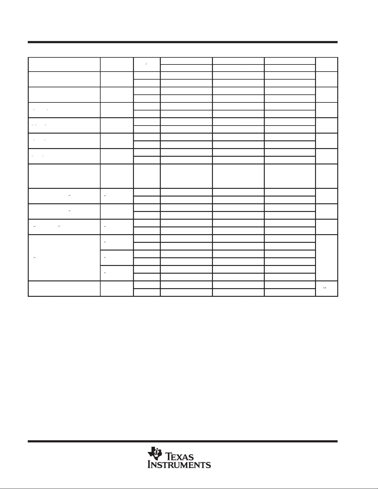
electrical characteristics at specified free-air temperature, VDD = 5 V
TEST
CONDITIONS
IT
(trigger)
(trigger)
(reset)
(reset)
OH
OL
†
Full range is 0
NOTE 2: These values apply for the expected operating configurations in which THRES is connected directly to DISCH or to TRIG.
Input threshold
voltage
reshold curren
gger voltage
gger curren
eset voltage
eset curren
Control voltage (open
circuit) as a
percentage of supply
voltage
Discharge switch
on-state voltage
Discharge switch
off-state current
High-level output
voltage
Low-level output
voltage
pp
OL
OH
OL
OL
OL
=
= –
=
=
=
°C to 70°C for TLC556C, –40°C to 85°C for TLC556I, and –55°C to 125°C for TLC556M.
A
25°C 2.8 3.3 3.8 2.8 3.3 3.8 2.8 3.3 3.8
Full range 2.7 3.9 2.7 3.9 2.7 3.9
25°C 10 10 10
MAX 75 150 5000
25°C 1.36 1.66 1.96 1.36 1.66 1.96 1.36 1.66 1.96
Full range 1.26 2.06 1.26 2.06 1.26 2.06
25°C 10 10 10
MAX 75 150 5000
25°C 0.4 1.1 1.5 0.4 1.1 1.5 0.4 1.1 1.5
Full range 0.3 1.8 0.3 1.8 0.3 1.8
25°C 10 10 10
MAX 75 150 5000
MAX 66.7% 66.7% 66.7%
25°C 0.15 0.5 0.15 0.5 0.15 0.5
Full range 0.6 0.6 0.6
25°C 0.1 0.1 0.1
MAX 0.5 2 120
25°C 4.1 4.8 4.1 4.8 4.1 4.8
Full range 4.1 4.1 4.1
25°C 0.21 0.4 0.21 0.4 0.21 0.4
Full range 0.5 0.5 0.6
25°C 0.13 0.3 0.13 0.3 0.13 0.3
Full range 0.4 0.4 0.45
25°C 0.08 0.3 0.08 0.3 0.08 0.3
Full range 0.35 0.35 0.4
25°C 340 700 340 700 340 700
Full range 1000 1200 1400
TLC556C TLC556I TLC556M
MIN TYP MAX MIN TYP MAX MIN TYP MAX
p
p
p
n
6
POST OFFICE BOX 655303 • DALLAS, TEXAS 75265
Page 7
PARAMETER
T
†
UNIT
VITInput threshold voltage
V
Threshold current
pA
V
Trigger voltage
V
I
Trigger current
pA
V
Reset voltage
V
I
Reset current
pA
g
I
100 mA
V
g
nA
I
10 mA
V
g
I
5 mA
V
I
1 mA
I
100 mA
V
I
50 mA
V
I
10 mA
IDDSupply current
See Note 2
mA
DUAL LinCMOS TIMERS
SLFS047B – FEBRUARY 1984 – REVISED SEPTEMBER 1997
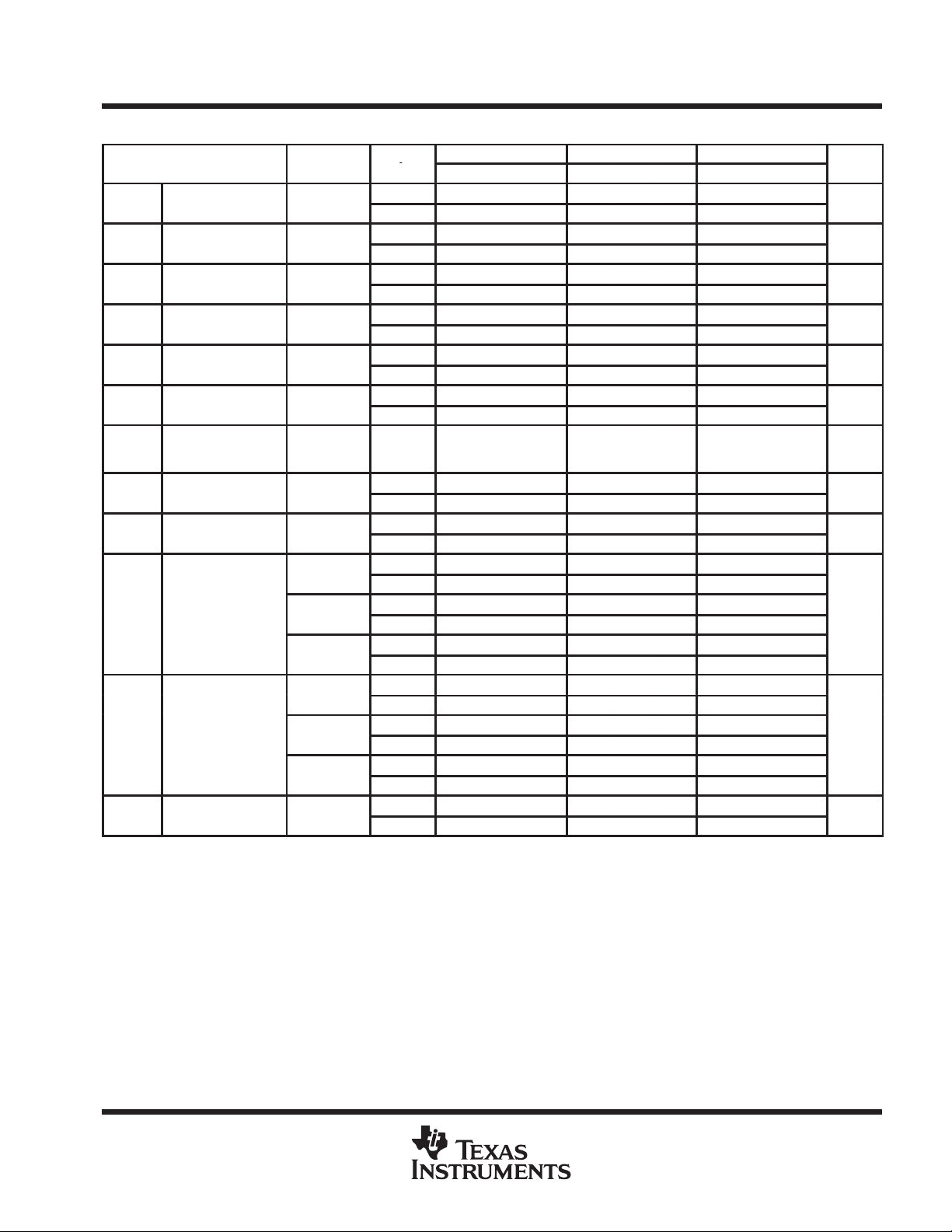
electrical characteristics at specified free-air temperature, VDD = 15 V
TEST
CONDITIONS
p
(trigger)
(trigger)
(reset)
(reset)
Control voltage (open
circuit) as a percentage of supply voltage
Discharge switch onstate voltage
Discharge switch offstate current
OH
OL
†
Full range is 0
NOTE 2: These values apply for the expected operating configurations in which THRES is connected directly to DISCH or TRIG.
High-level output
voltage
Low-level output
voltage
pp
°C to 70°C for TLC556C, –40°C to 85°C for TLC556I, and –55°C to 125°C for TLC556M.
OL
OH
OH
OH
OL
OL
OL
=
= –
= –
= –
=
=
=
A
25°C
Full range 9.35 10.65 9.35 10.65 9.35 10.65
25°C
MAX 75 150 5000
25°C
Full range 4.55 5.45 4.55 5.45 4.55 5.45
25°C
MAX 75 150 5000
25°C
Full range 0.3 1.8 0.3 1.8 0.3 1.8
25°C
MAX 75 150 5000
MAX 66.7% 66.7% 66.7%
25°C
Full range 1.8 1.8 1.8
25°C
MAX 0.5 2 120
25°C
Full range 12.5 12.5 12.5
25°C
Full range 13.5 13.5 13.5
25°C
Full range 14.2 14.2 14.2
25°C
Full range 3.6 3.7 3.8
25°C
Full range 1.3 1.4 1.5
25°C
Full range 0.4 0.4 0.45
25°C
Full range 1.6 1.8 2
TLC556C TLC556I TLC556M
MIN TYP MAX MIN TYP MAX MIN TYP MAX
9.45 10 10.55 9.45 10 10.55 9.45 10 10.55
10 10 10
4.65 5 5.35 4.65 5 5.35 4.65 5 5.35
10 10 10
0.4 1.1 1.5 0.4 1.1 1.5 0.4 1.1 1.5
10 10 10
0.8 1.7 0.8 1.7 0.8 1.7
0.1 0.1 0.1
12.5 14.2 12.5 14.2 12.5 14.2
13.5 14.6 13.5 14.6 13.5 14.6
14.2 14.9 14.2 14.9 14.2 14.9
1.28 3.2 1.28 3.2 1.28 3.2
0.63 1 0.63 1 0.63 1
0.12 0.3 0.12 0.3 0.12 0.3
0.72 1.2 0.72 1.2 0.72 1.2
TLC556, TLC556Y
p
p
p
POST OFFICE BOX 655303 • DALLAS, TEXAS 75265
7
Page 8
TLC556, TLC556Y
R
C
pF
ns
DUAL LinCMOS TIMERS
SLFS047B – FEBRUARY 1984 – REVISED SEPTEMBER 1997
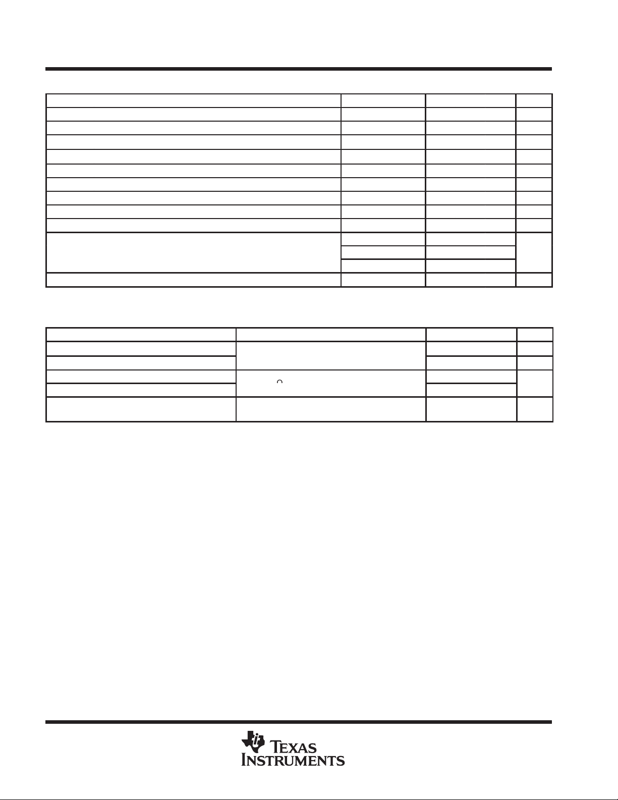
electrical characteristics, V
PARAMETER TEST CONDITIONS MIN TYP MAX UNIT
V
IT
V
(trigger)
I
(trigger)
V
(reset)
I
(reset)
V
OH
V
OL
I
DD
NOTE 2: These values apply for the expected operating configurations in which THRES is connected directly to DISCH or TRIG.
Input threshold voltage 2.8 3.3 3.8 V
Threshold current 10 pA
Trigger voltage 1.36 1.66 1.96 V
Trigger current 10 pA
Reset voltage 0.4 1.1 1.5 V
Reset current 10 pA
Discharge switch on-state voltage IOL = 10 mA 0.15 0.5 V
Discharge switch off-state current 0.1 nA
High-level output voltage IOH = –1 mA 4.1 4.8 V
Low-level output voltage
Supply current See Note 2 3.40 700 µA
= 5 V, TA = 25°C
DD
IOL = 8 mA 0.21 0.4
IOL = 5 mA
IOL = 2.1 mA 0.08 0.3
0.13 0.3
V
operating characteristics, VDD = 5 V, TA = 25°C (unless otherwise noted)
PARAMETER TEST CONDITIONS MIN TYP MAX UNIT
Initial error of timing interval
Supply voltage sensitivity of timing interval
t
Output pulse rise time
r
t
Output pulse fall time
f
f
Maximum frequency in astable mode
max
†
Timing interval error is defined as the difference between the measured value and the average value of a random sample from each process
run.
NOTE 3: RA, RB, and CT are as defined in Figure 3.
†
VDD = 5 V to 15 V, RA = RB = 1 kΩ to 100 kΩ 1% 3%
CT = 0.1 µF, See Note 3 0.1 0.5 %/V
= 10 MΩ,
L
RA = 470 Ω,
CT = 200 pF,
p
= 10
L
RB = 200 Ω,
See Note 3
1.2 2.1 MHz
20 75
15 60
8
POST OFFICE BOX 655303 • DALLAS, TEXAS 75265
Page 9
TLC556, TLC556Y
DUAL LinCMOS TIMERS
SLFS047B – FEBRUARY 1984 – REVISED SEPTEMBER 1997
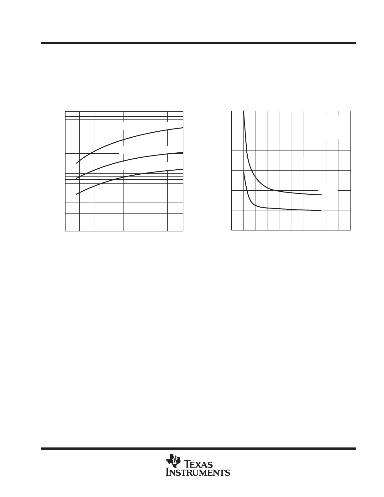
TYPICAL CHARACTERISTICS
PROPAGATION DELAY TIMES (TO DISCHARGE
OUTPUT FROM TRIGGER AND THRESHOLD
SHORTED TOGETHER)
DISCHARGE SWITCH ON-STATE RESISTANCE
vs
FREE-AIR TEMPERATURE
100
70
Ω
40
VDD = 2 V, IO = 1 mA
SUPPLY VOLTAGE
600
500
vs
I
≥ 1 mA
O(on)
CL ≈ 0
TA = 25°C
20
10
7
4
2
Discharge Switch On-State Resistance –
1
–75 –50 –25 0 25 75 125
TA – Free-Air Temperature – °C
VDD = 5 V, IO = 10 mA
VDD = 15 V, IO = 100 mA
50 100
Figure 1
400
300
t
t
PLH
PHL
‡
200
PLH
t – Propagation Delay Times – ns
100
PHL
t,
0
0 2 4 6 8 12 16
VDD – Supply Voltage – V
‡
The effects of the load resistance on these values must be
taken into account separately.
10 14
Figure 2
2018
POST OFFICE BOX 655303 • DALLAS, TEXAS 75265
9
Page 10
TLC556, TLC556Y
DUAL LinCMOS TIMERS
SLFS047B – FEBRUARY 1984 – REVISED SEPTEMBER 1997
APPLICATION INFORMATION
0.1 µF
R
A
R
B
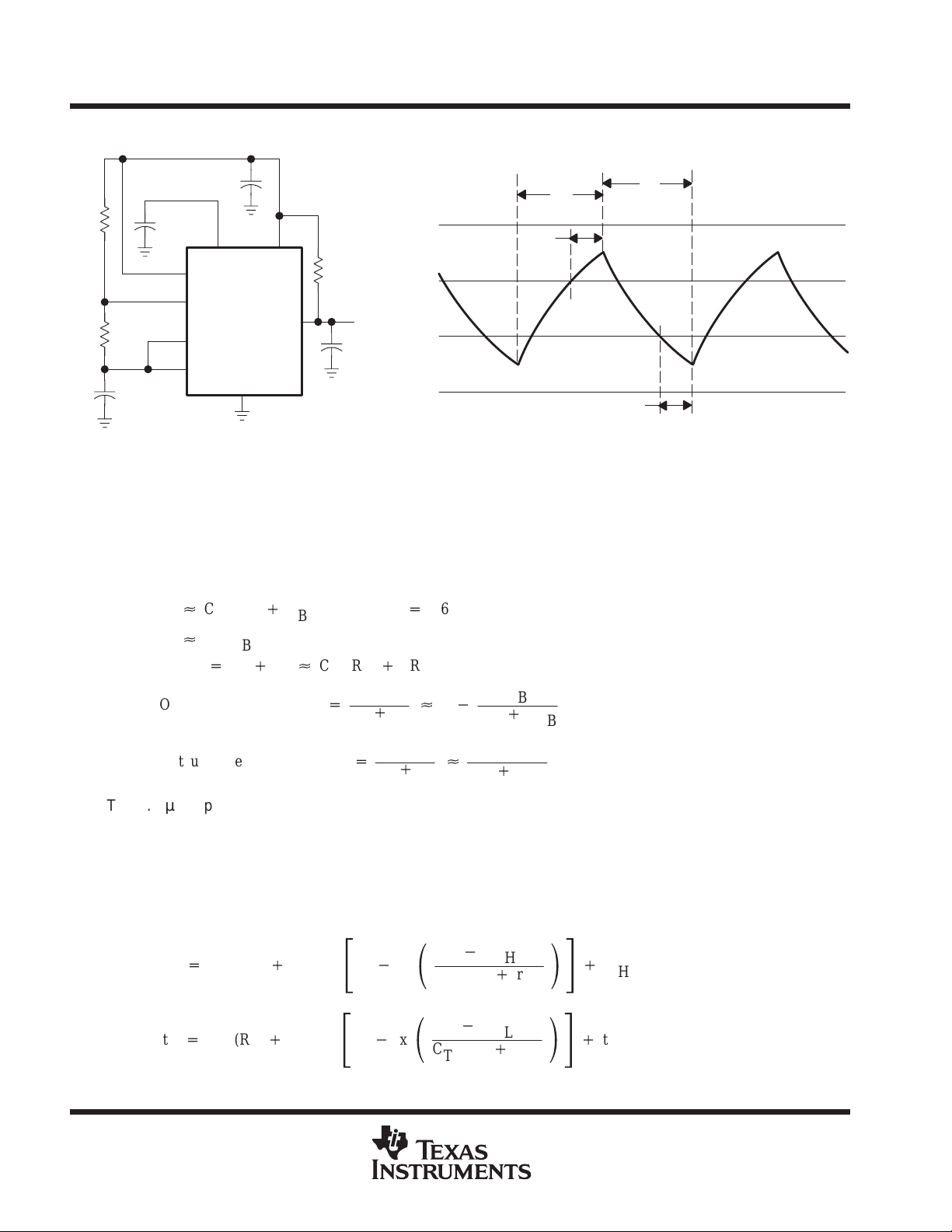
Connecting the trigger input to the threshold input, as shown in Figure 3, causes the timer to run as a
multivibrator. The capacitor C
V
DD
The output is high during the charging cycle (tH) and low during the discharge cycle (tL). The duty cycle is
controlled by the values of RA, and RB, and CT, as shown in the equations below.
0.1 µF
CONT V
RESET
TLC556
DISCH
THRES
TRIG
C
T
CIRCUIT TRIGGER AND THRESHOLD VOLTAGE WAVEFORM
) and then discharges through RB only to the value of the trigger voltage level (approximately 0.33 VDD).
tH[
CT(RA)
GND
DD
OUT
R
L
Output
C
L
Figure 3. Astable Operation
charges through RA and RB to the threshold voltage level (approximately 0.67
T
RB) In 2 (In 2+0.693)
2/3 V
1/3 V
V
DD
DD
DD
GND
t
PHL
t
H
t
PLH
t
L
tL[
CTRBIn 2
Period+tH)
Output driver duty cycle
Output waveform duty cycle
The 0.1-µF capacitor at CONT in Figure 3 decreases the period by about 10%.
The formulas shown above do not allow for any propagation delay from the trigger and threshold inputs to the
discharge output. These delay times add directly to the period and create differences between calculated and
actual values that increase with frequency . In addition, the discharge output resistance r
another source of error in the calculation when RB is very low or ron is very high.
The equations below provide better agreement with measured values.
tH+
tL+
CT(RA)
CT(RB)
tL[
CT(RA)
t
+
tH)
+
RB)Inƪ3*exp
ron)Inƪ3*exp
2RB)In2
L
t
L
t
H
tH)
[1*
[
t
L
*
ǒ
CT(RB)
*
ǒ
CT(RA)
RA)
R
RA)
t
PLH
t
PHL
R
B
B
2R
2R
ron)
RB)
B
B
adds to RB to provide
on
Ǔ
)
t
ƫ
PHL
Ǔ
)
t
ƫ
PLH
10
POST OFFICE BOX 655303 • DALLAS, TEXAS 75265
Page 11

TLC556, TLC556Y
DUAL LinCMOS TIMERS
SLFS047B – FEBRUARY 1984 – REVISED SEPTEMBER 1997
APPLICATION INFORMATION
The preceding equations and those given earlier are similar in that a time constant is multiplied by the logarithm
of a number or function. The limit values of the logarithmic terms must be between In 2 at low frequencies and
In 3 at extremely high frequencies. For a duty cycle close to 50%, an appropriate constant for the logarithmic
t
terms can be substituted with good results. Duty cycles less than 50%
possibly RA ≤ ron. These conditions can be difficult to obtain.
In monostable applications, the trip point of the trigger input can be set by a voltage applied to CONT. An input
voltage between 10% and 80% of the supply voltage from a resistor divider with at least 500-µA bias provides
good results.
tH)
H
will require that
t
L
t
H
< 1 and
t
L
POST OFFICE BOX 655303 • DALLAS, TEXAS 75265
11
Page 12
PACKAGE OPTION ADDENDUM
www.ti.com
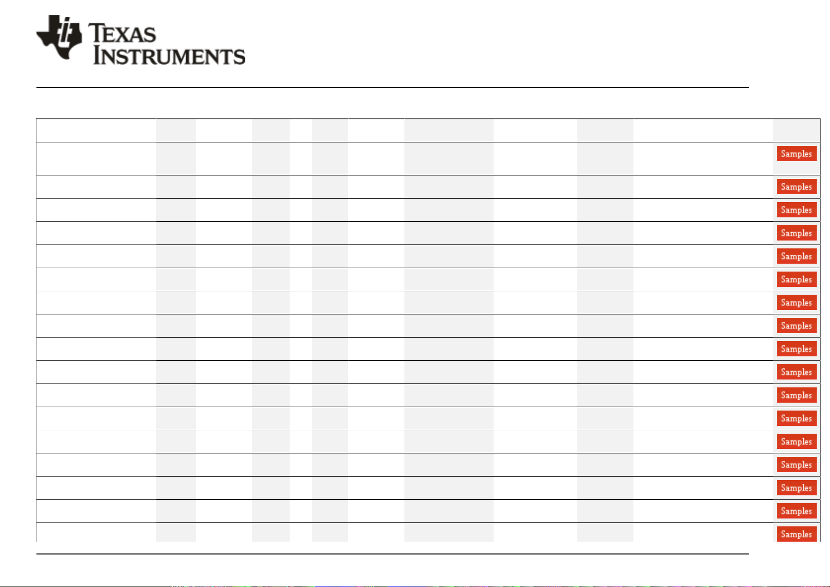
PACKAGING INFORMATION
Orderable Device Status
5962-89503022A ACTIVE LCCC FK 20 1 TBD POST-PLATE N / A for Pkg Type -55 to 125 5962-
5962-8950302CA ACTIVE CDIP J 14 1 TBD Call TI N / A for Pkg Type -55 to 125 5962-8950302CA
TLC556CD ACTIVE SOIC D 14 50 Green (RoHS
TLC556CDG4 ACTIVE SOIC D 14 50 Green (RoHS
TLC556CDR ACTIVE SOIC D 14 2500 Green (RoHS
TLC556CDRG4 ACTIVE SOIC D 14 2500 Green (RoHS
TLC556CN ACTIVE PDIP N 14 25 Green (RoHS
TLC556ID ACTIVE SOIC D 14 50 Green (RoHS
TLC556IDG4 ACTIVE SOIC D 14 50 Green (RoHS
TLC556IDR ACTIVE SOIC D 14 2500 Green (RoHS
TLC556IDRG4 ACTIVE SOIC D 14 2500 Green (RoHS
TLC556IN ACTIVE PDIP N 14 25 Green (RoHS
TLC556MD ACTIVE SOIC D 14 50 Green (RoHS
TLC556MDG4 ACTIVE SOIC D 14 50 Green (RoHS
TLC556MDR ACTIVE SOIC D 14 2500 Green (RoHS
TLC556MDRG4 ACTIVE SOIC D 14 50 Green (RoHS
TLC556MFKB ACTIVE LCCC FK 20 1 TBD POST-PLATE N / A for Pkg Type -55 to 125 5962-
Package Type Package
(1)
Drawing
Pins Package
Qty
Eco Plan
(2)
& no Sb/Br)
& no Sb/Br)
& no Sb/Br)
& no Sb/Br)
& no Sb/Br)
& no Sb/Br)
& no Sb/Br)
& no Sb/Br)
& no Sb/Br)
& no Sb/Br)
& no Sb/Br)
& no Sb/Br)
& no Sb/Br)
& no Sb/Br)
Lead/Ball Finish
(6)
MSL Peak Temp
(3)
Op Temp (°C) Device Marking
NIPDAU Level-1-260C-UNLIM 0 to 70 TLC556C
NIPDAU Level-1-260C-UNLIM 0 to 70 TLC556C
NIPDAU Level-1-260C-UNLIM TLC556C
NIPDAU Level-1-260C-UNLIM TLC556C
NIPDAU N / A for Pkg Type TLC556CN
NIPDAU Level-1-260C-UNLIM TLC556I
NIPDAU Level-1-260C-UNLIM TLC556I
NIPDAU Level-1-260C-UNLIM -40 to 85 TLC556I
NIPDAU Level-1-260C-UNLIM -40 to 85 TLC556I
NIPDAU N / A for Pkg Type TLC556IN
NIPDAU Level-1-260C-UNLIM -55 to 125 TLC556M
NIPDAU Level-1-260C-UNLIM TLC556M
NIPDAU Level-1-260C-UNLIM -55 to 125 TLC556M
NIPDAU Level-1-260C-UNLIM TLC556M
6-Feb-2020
Samples
(4/5)
89503022A
TLC556MFKB
TLC556MJB
Addendum-Page 1
Page 13
PACKAGE OPTION ADDENDUM
www.ti.com
Orderable Device Status
TLC556MJ ACTIVE CDIP J 14 1 TBD Call TI N / A for Pkg Type -55 to 125 TLC556MJ
TLC556MJB ACTIVE CDIP J 14 1 TBD Call TI N / A for Pkg Type -55 to 125 5962-8950302CA
(1)
The marketing status values are defined as follows:
ACTIVE: Product device recommended for new designs.
LIFEBUY: TI has announced that the device will be discontinued, and a lifetime-buy period is in effect.
NRND: Not recommended for new designs. Device is in production to support existing customers, but TI does not recommend using this part in a new design.
PREVIEW: Device has been announced but is not in production. Samples may or may not be available.
OBSOLETE: TI has discontinued the production of the device.
Package Type Package
(1)
Drawing
Pins Package
Qty
Eco Plan
(2)
Lead/Ball Finish
(6)
MSL Peak Temp
(3)
Op Temp (°C) Device Marking
(4/5)
89503022A
TLC556MFKB
TLC556MJB
(2)
RoHS: TI defines "RoHS" to mean semiconductor products that are compliant with the current EU RoHS requirements for all 10 RoHS substances, including the requirement that RoHS substance
do not exceed 0.1% by weight in homogeneous materials. Where designed to be soldered at high temperatures, "RoHS" products are suitable for use in specified lead-free processes. TI may
reference these types of products as "Pb-Free".
RoHS Exempt: TI defines "RoHS Exempt" to mean products that contain lead but are compliant with EU RoHS pursuant to a specific EU RoHS exemption.
Green: TI defines "Green" to mean the content of Chlorine (Cl) and Bromine (Br) based flame retardants meet JS709B low halogen requirements of <=1000ppm threshold. Antimony trioxide based
flame retardants must also meet the <=1000ppm threshold requirement.
(3)
MSL, Peak Temp. - The Moisture Sensitivity Level rating according to the JEDEC industry standard classifications, and peak solder temperature.
(4)
There may be additional marking, which relates to the logo, the lot trace code information, or the environmental category on the device.
(5)
Multiple Device Markings will be inside parentheses. Only one Device Marking contained in parentheses and separated by a "~" will appear on a device. If a line is indented then it is a continuation
of the previous line and the two combined represent the entire Device Marking for that device.
(6)
Lead/Ball Finish - Orderable Devices may have multiple material finish options. Finish options are separated by a vertical ruled line. Lead/Ball Finish values may wrap to two lines if the finish
value exceeds the maximum column width.
Important Information and Disclaimer:The information provided on this page represents TI's knowledge and belief as of the date that it is provided. TI bases its knowledge and belief on information
provided by third parties, and makes no representation or warranty as to the accuracy of such information. Efforts are underway to better integrate information from third parties. TI has taken and
continues to take reasonable steps to provide representative and accurate information but may not have conducted destructive testing or chemical analysis on incoming materials and chemicals.
TI and TI suppliers consider certain information to be proprietary, and thus CAS numbers and other limited information may not be available for release.
In no event shall TI's liability arising out of such information exceed the total purchase price of the TI part(s) at issue in this document sold by TI to Customer on an annual basis.
6-Feb-2020
Samples
Addendum-Page 2
Page 14
PACKAGE OPTION ADDENDUM
www.ti.com
OTHER QUALIFIED VERSIONS OF TLC556, TLC556M :
Catalog: TLC556
•
Military: TLC556M
•
NOTE: Qualified Version Definitions:
Catalog - TI's standard catalog product
•
Military - QML certified for Military and Defense Applications
•
6-Feb-2020
Addendum-Page 3
Page 15
PACKAGE MATERIALS INFORMATION
www.ti.com 26-Feb-2019
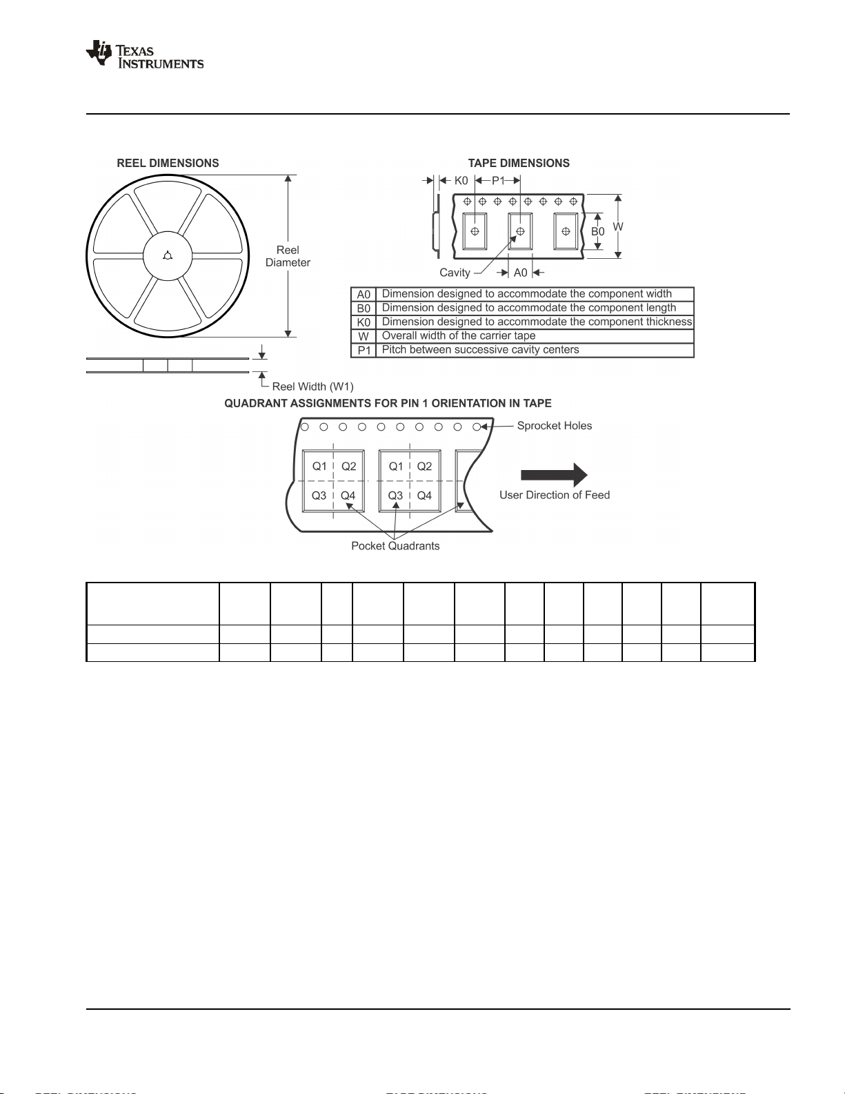
TAPE AND REEL INFORMATION
*All dimensions are nominal
Device Package
TLC556CDR SOIC D 14 2500 330.0 16.4 6.5 9.0 2.1 8.0 16.0 Q1
TLC556IDR SOIC D 14 2500 330.0 16.4 6.5 9.0 2.1 8.0 16.0 Q1
Type
Package
Drawing
Pins SPQ Reel
Diameter
(mm)
Reel
Width
W1 (mm)
A0
(mm)B0(mm)K0(mm)P1(mm)W(mm)
Pin1
Quadrant
Pack Materials-Page 1
Page 16
PACKAGE MATERIALS INFORMATION
www.ti.com 26-Feb-2019
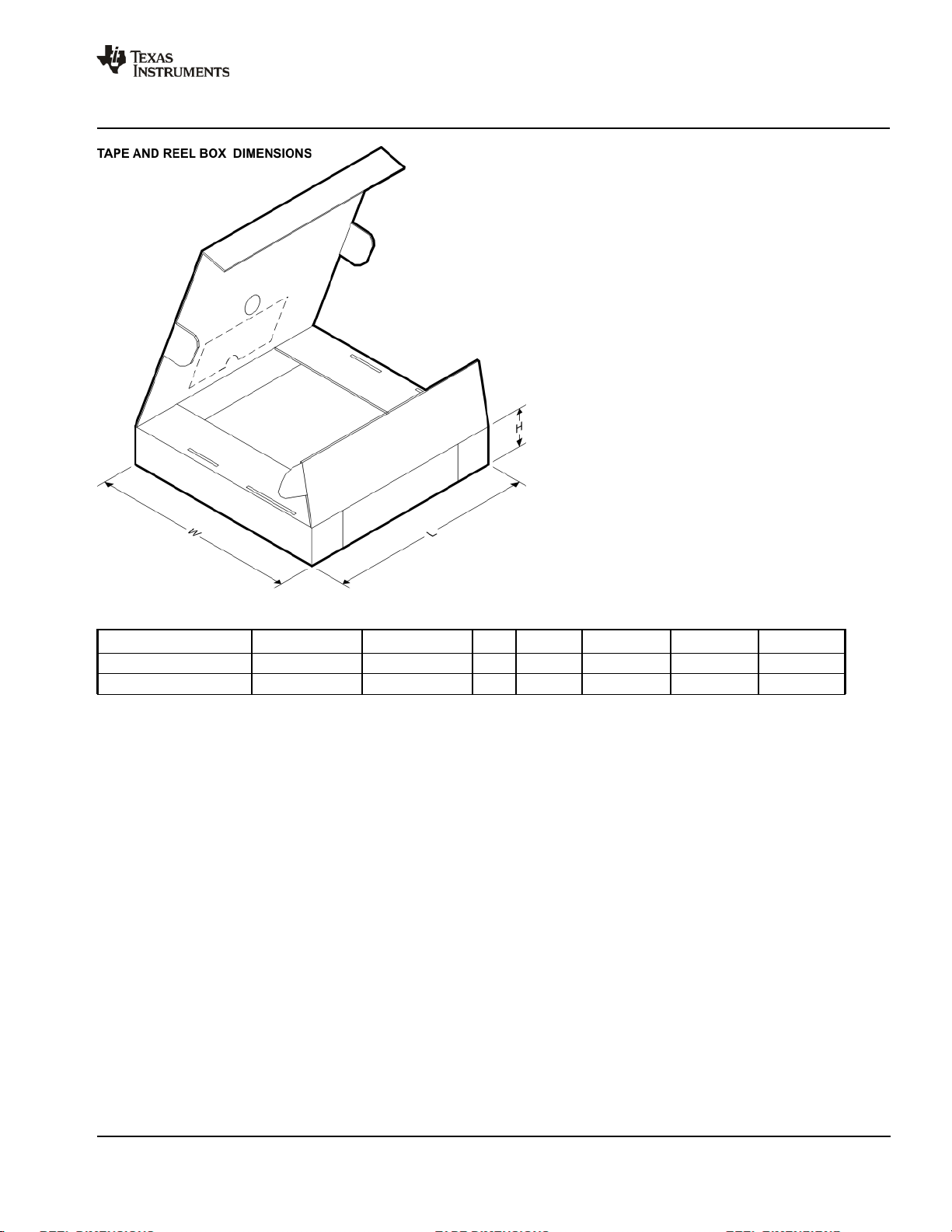
*All dimensions are nominal
Device Package Type Package Drawing Pins SPQ Length (mm) Width (mm) Height (mm)
TLC556CDR SOIC D 14 2500 333.2 345.9 28.6
TLC556IDR SOIC D 14 2500 350.0 350.0 43.0
Pack Materials-Page 2
Page 17
Page 18
Page 19
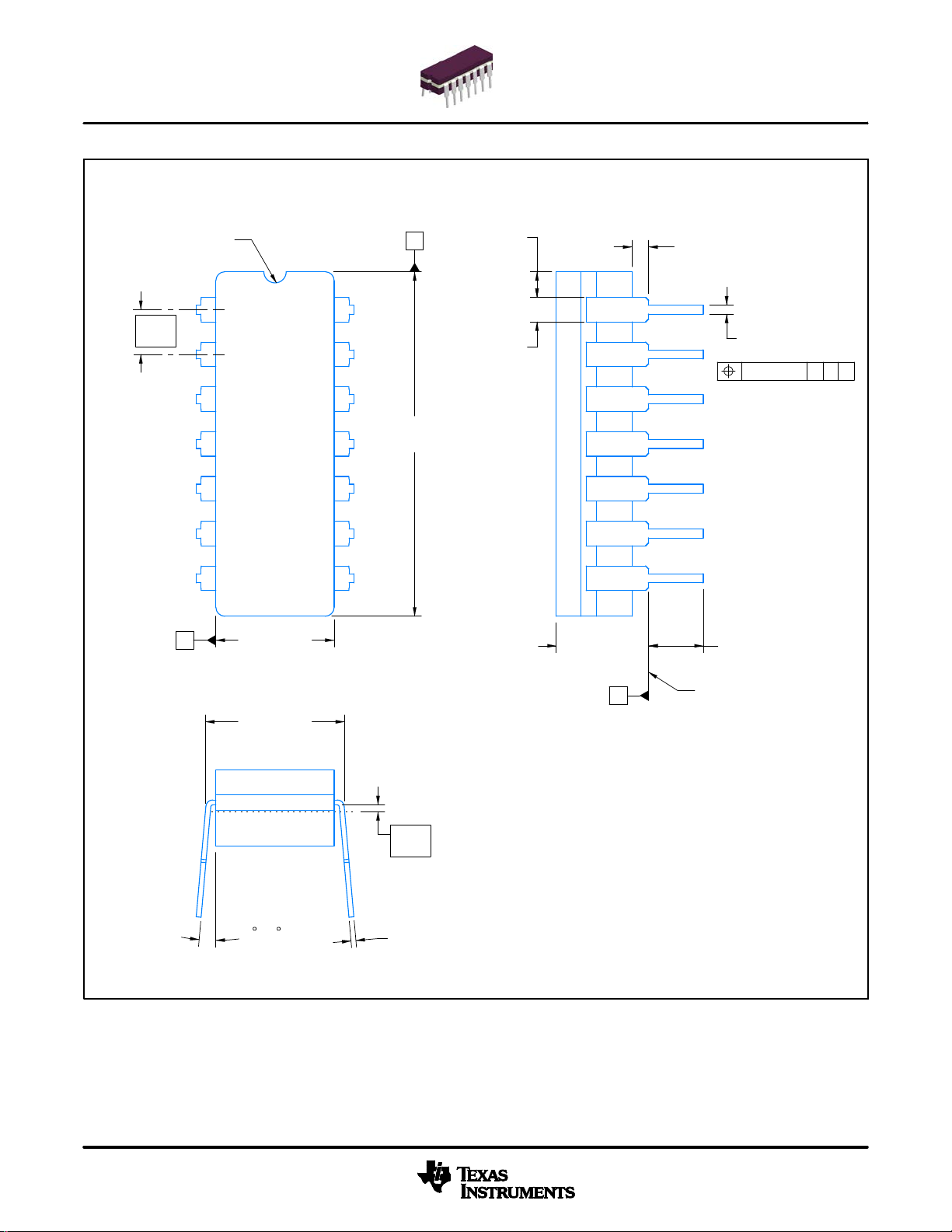
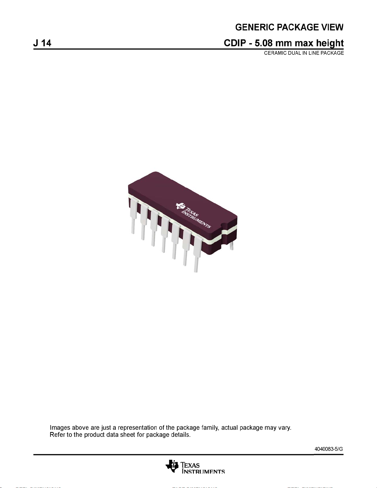
PACKAGE OUTLINE
12X .100
[2.54]
PIN 1 ID
(OPTIONAL)
1
14
A
-.785.754
-19.9419.15[ ]
SCALE 0.900
4X .005 MIN
14X -.065.045
[0.13]
-1.651.15[ ]
CDIP - 5.08 mm max heightJ0014A
CERAMIC DUAL IN LINE PACKAGE
TYP-.060.015
-1.520.38[ ]
14X -.026.014
-0.660.36[ ]
.010 [0.25] C A B
7
B -.283.245
AT GAGE PLANE
NOTES:
1. All controlling linear dimensions are in inches. Dimensions in brackets are in millimeters. Any dimension in brackets or parenthesis are for
reference only. Dimensioning and tolerancing per ASME Y14.5M.
2. This drawing is subject to change without notice.
3. This package is hermitically sealed with a ceramic lid using glass frit.
4. Index point is provided on cap for terminal identification only and on press ceramic glass frit seal only.
5. Falls within MIL-STD-1835 and GDIP1-T14.
0
-7.196.22[ ]
-.314.308
-7.977.83[ ]
-15
TYP
8
.015 GAGE PLANE
[0.38]
14X .008-.014
[0.2-0.36]
.2 MAX TYP
[5.08]
C
.13 MIN TYP
[3.3]
SEATING PLANE
4214771/A 05/2017
www.ti.com
Page 20
SEE DETAIL A
(.300 ) TYP
[7.62]
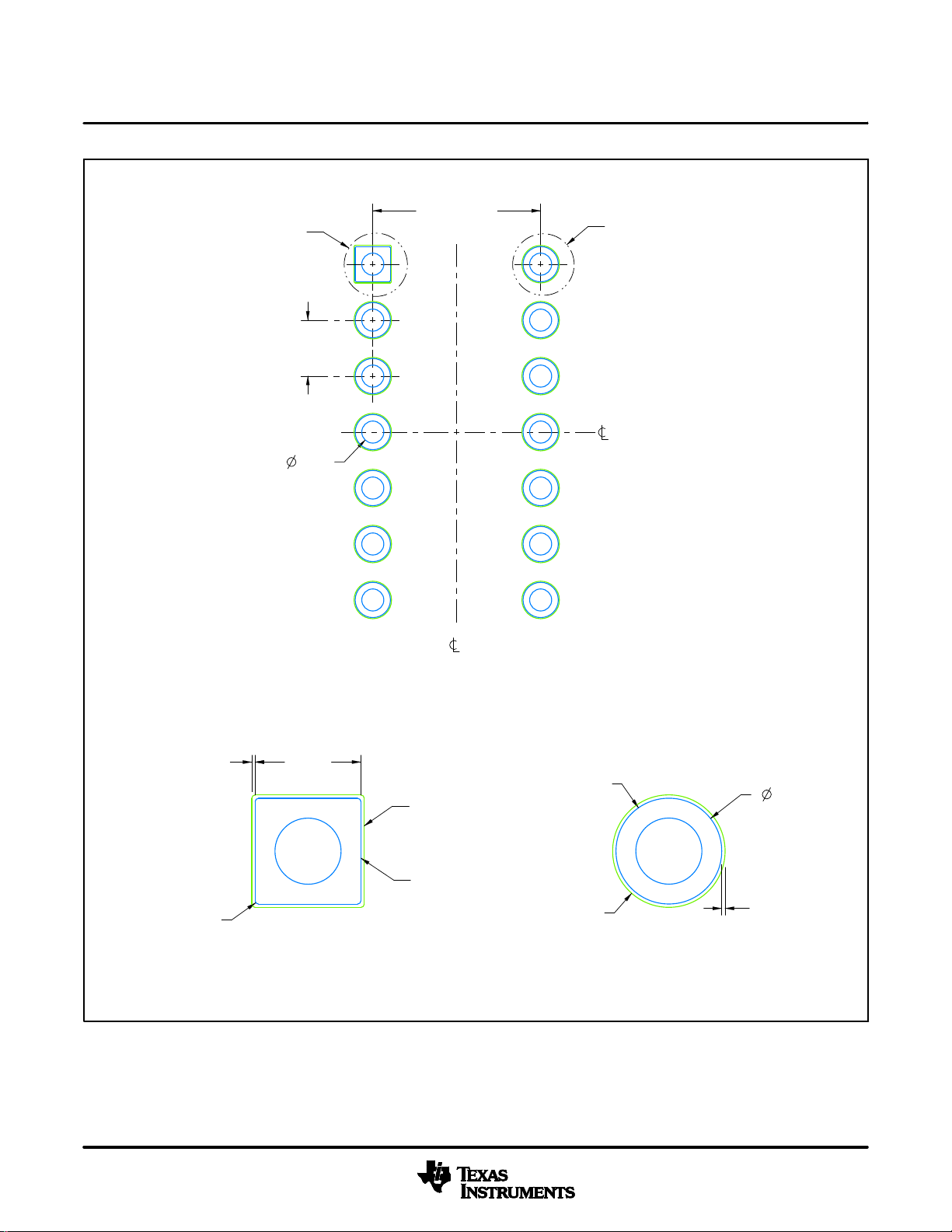
EXAMPLE BOARD LAYOUT
CDIP - 5.08 mm max heightJ0014A
CERAMIC DUAL IN LINE PACKAGE
SEE DETAIL B
12X (.100 )
[2.54]
14X ( .039)
[1]
1
7
SYMM
LAND PATTERN EXAMPLE
NON-SOLDER MASK DEFINED
SCALE: 5X
14
SYMM
8
MAX.002
[0.05]
ALL AROUND
(R.002 ) TYP
[0.05]
(.063)
[1.6]
DETAIL A
SCALE: 15X
SOLDER MASK
OPENING
METAL
www.ti.com
METAL
SOLDER MASK
OPENING
( .063)
[1.6]
.002 MAX
[0.05]
ALL AROUND
DETAIL B
13X, SCALE: 15X
4214771/A 05/2017
Page 21
Page 22
Page 23
Page 24

IMPORTANT NOTICE AND DISCLAIMER
TI PROVIDES TECHNICAL AND RELIABILITY DATA (INCLUDING DATASHEETS), DESIGN RESOURCES (INCLUDING REFERENCE
DESIGNS), APPLICATION OR OTHER DESIGN ADVICE, WEB TOOLS, SAFETY INFORMATION, AND OTHER RESOURCES “AS IS”
AND WITH ALL FAULTS, AND DISCLAIMS ALL WARRANTIES, EXPRESS AND IMPLIED, INCLUDING WITHOUT LIMITATION ANY
IMPLIED WARRANTIES OF MERCHANTABILITY, FITNESS FOR A PARTICULAR PURPOSE OR NON-INFRINGEMENT OF THIRD
PARTY INTELLECTUAL PROPERTY RIGHTS.
These resources are intended for skilled developers designing with TI products. You are solely responsible for (1) selecting the appropriate
TI products for your application, (2) designing, validating and testing your application, and (3) ensuring your application meets applicable
standards, and any other safety, security, or other requirements. These resources are subject to change without notice. TI grants you
permission to use these resources only for development of an application that uses the TI products described in the resource. Other
reproduction and display of these resources is prohibited. No license is granted to any other TI intellectual property right or to any third
party intellectual property right. TI disclaims responsibility for, and you will fully indemnify TI and its representatives against, any claims,
damages, costs, losses, and liabilities arising out of your use of these resources.
TI’s products are provided subject to TI’s Terms of Sale (www.ti.com/legal/termsofsale.html) or other applicable terms available either on
ti.com or provided in conjunction with such TI products. TI’s provision of these resources does not expand or otherwise alter TI’s applicable
warranties or warranty disclaimers for TI products.
Mailing Address: Texas Instruments, Post Office Box 655303, Dallas, Texas 75265
Copyright © 2020, Texas Instruments Incorporated
 Loading...