

Datasheet TS27L4IP, TS27L4IDT, TS27L4CP, TS27L4CPT, TS27L4AIDT Datasheet (SGS Thomson Microelectronics)
...Page 1
1/9
■ VERY LOW POWER CONSUMPTION :
10µA/op
■ OUTPUT VOLTAGE CAN SWING TO
GROUND
■ EXCELLENT PHASE MARGIN ON
CAPACITIVE LOADS
■ STABLE AND LOW OF FSET VOLTAGE
■ THREE INPUT OFFSET VOLTAGE
SELECTIONS
DESCRIPTION
These devices are low cost, low power quad operational amplifiers designed to operate with single
or dual supplies. These operational amplifiers use
the ST silicon gate CMOS process allowing an excellent consumption-speed ratio. These series are
ideally suited for low consumption applications.
Three power consumpt ions are av ailable a llowing
to have always the best consumption-speed ratio:
❑ I
CC
= 10µA/amp.: TS27L4 (very low power)
❑ I
CC
= 150µA/amp.: TS27M4 (low power)
❑ I
CC
= 1mA/amp.: TS274 (standard)
These CMOS amplifiers offer very high input impedance and extremely low input currents. The
major advantage versus JFET devices is the very
low input currents drift with temperature (see figure 2 ).
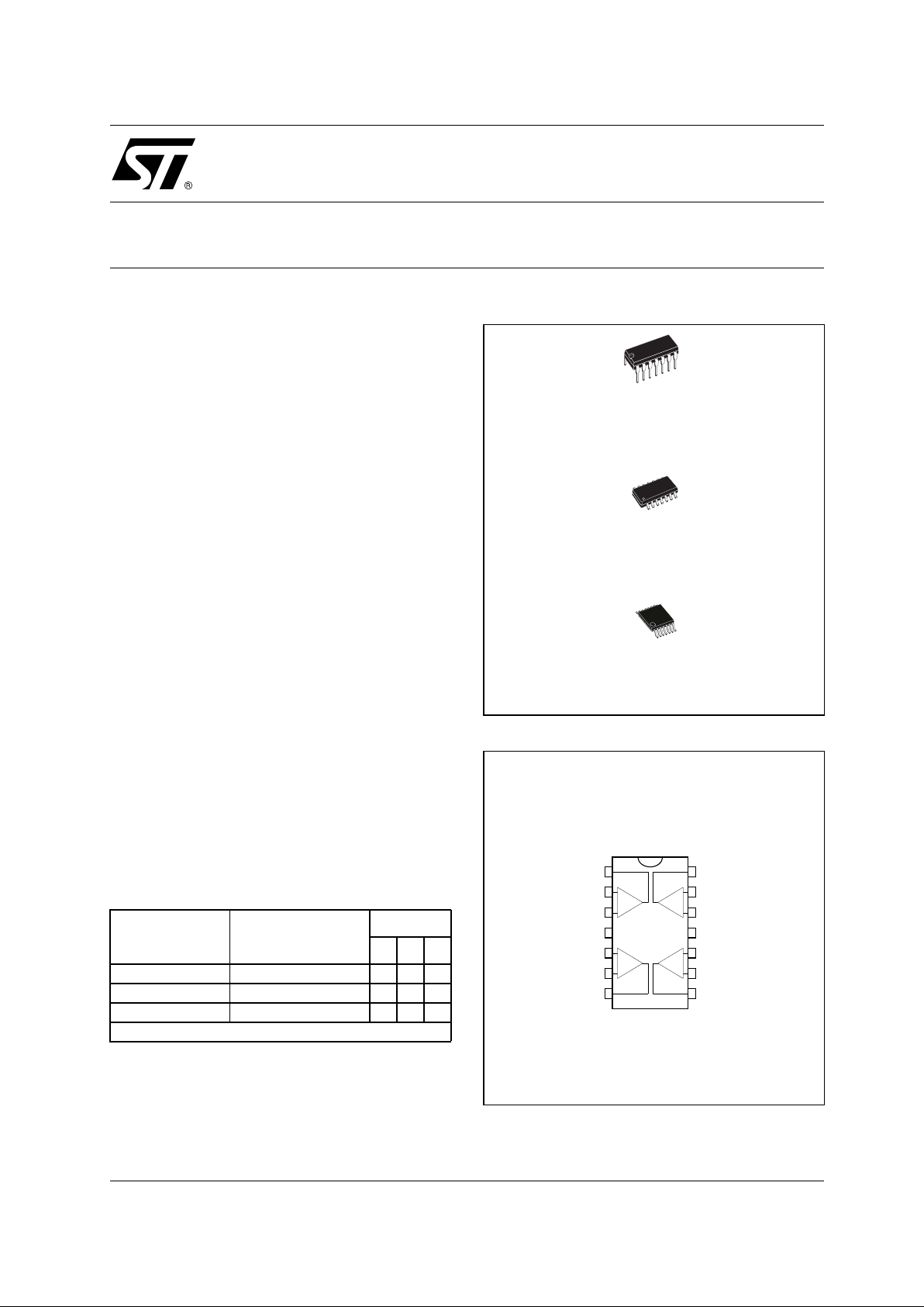
ORDER CODE
N = Dual in Line Package (DIP)
D = Small Outline Package (SO) - also available in Tape & Reel (DT)
P = Thin Shrink Small Outline Package (TSSOP) - only available
in Tape & Reel (PT)
* TS27L4BID : For deli very informati on, please cont act your ST sal es
representative or distributor.
PIN CONNECTIONS (top view)
Part Number Temperature Range
Package
NDP
TS27L4C/AC/BC 0°C, +70°C
•••
TS27L4I/AI/BI* -40°C, +125°C
•••
TS27L4M/AM/BM -55°C, +125°C
•••
Example : TS27L4ACN
N
DIP14
(Plastic Package)
D
SO14
(Plastic Micropackage)
P
TSSOP14
(Thin Shrink Small Outline Package)
Inverting Input 2
Non-inverting Input 2
Non-inverting Input 1
CC
V
-
CC
V
1
2
3
4
8
5
6
7
9
10
11
12
13
14
+
Output 3
Output 4
Non-inverting Input 4
Inverting Input 4
Non-inverting Input 3
Inverting Input 3
-
+
+
-
+
-
+
Output 1
Inverting Input 1
Output 2
TS27L4C,I,M
PRECISION VERY LOW POWER CMOS
QUAD OPERATIONAL AMPLIFIER
June 2003
Page 2
TS27L4C,I,M
2/9
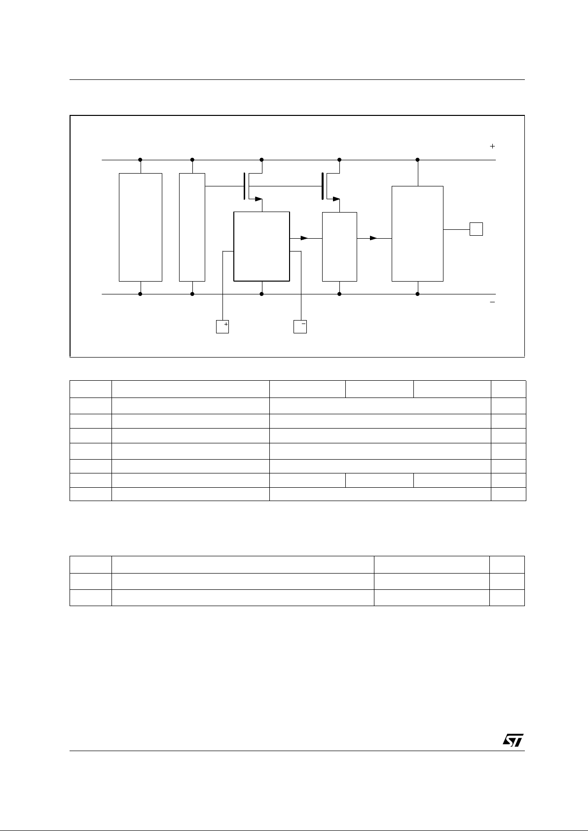
BLOCK DIAGRAM
ABSOLUTE MAXIMUM RATINGS
OPERATING CONDITIONS
E
E
Input
differential
Second
stage
Output
stage
Output
CC
V
CC
V
Current
source
x I
Symbol Parameter TS27L4C/AC/BC TS27L4I/AI/BI TS27L4M/AM/BM Unit
V
CC
+
Supply Voltage
1)
18 V
V
id
Differential Input Voltage
2)
±18 V
V
i
Input Voltage
3)
-0.3 to 18 V
I
o
Output Current for V
CC
+
≥ 15V
±30 mA
I
in
Input Current ±5 mA
T
oper
Operating Free-Air Temperature Range 0 to +70 -40 to +125 -55 to +125 °C
T
stg
Storage Temperature Range -65 to +150 °C
1. All values, except differential voltage are with respect to network ground terminal.
2. Dif ferential voltages are the non-inv erting input terminal with respec t to t he i nverting i nput terminal .
3. The magnitud e of the input an d the output voltages must never excee d the magnit ude of the posi tive suppl y v ol tage.
Symbol Parameter Value Unit
V
CC
+
Supply Voltage 3 to 16 V
V
icm
Common Mode Input Voltage Range
0 to V
CC
+
- 1.5
V
Page 3
TS27L4C,I,M
3/9
SCHEMATIC DIAGRAM (for 1/4 TS27L4)
T
T
25
2
T
17 18
R
T
20
T
21
T
T
23
22
Input
Output
T
24
T
19
V
CC
V
CC
T
26
T
27
T
28
T
29
Input
T
3
T
4
T
5
T
2
T
1
R1
C1
T
7
T
6
T
8
T
9
T
13
T
14
T
11
T
12
T
10
T
16
T
15
Page 4

TS27L4C,I,M
4/9
ELECTRICAL CHARACTERISTICS
V
CC
+
= +10V, V
CC
-
= 0V, T
amb
= +25°C (unless otherwise specified)
Symbol Parameter
TS27L4C/AC/BC
TS27L4I/AI/BI
TS27L4M/AM/BM
Unit
Min. Typ. Max. Min. Typ. Max.
V
io
Input Offset Voltage
V
O
= 1.4V, Vic = 0V TS27L4C/I/M
TS27L4AC/AI/AM
TS27L4B/C/I/M
T
min
≤ T
amb
≤ T
max
TS27L4C/I/M
TS27L4AC/AI/AM
TS27L4B/C/I/M
1.1
0.9
0.25
10
5
2
12
6.5
3
1.1
0.9
0.25
10
5
2
12
6.5
3.5
mV
DV
io
Input Offset Voltage Drift 2 2 µV/°C
I
io
Input Offset Current note
1)
Vic = 5V, VO = 5V
T
min
≤ T
amb
≤ T
max
1. Maximum values including unavoidable inaccuracies of the industrial test.
1
100
1
200
pA
I
ib
Input Bias Current - see note 1
Vic = 5V, VO = 5V
T
min
≤ T
amb
≤ T
max
1
150
1
300
pA
V
OH
High Level Output Voltage
V
id
= 100mV, RL = 1M
Ω
T
min
≤ T
amb
≤ T
max
8.8
8.7
98.8
8.6
9V
V
OL
Low Level Output Voltage
V
id
= -100mV
50 50
mV
A
vd
Large Signal Voltage Gain
V
iC
= 5V, RL = 1M
Ω,
Vo = 1V to 6V
T
min
≤ T
amb
≤ T
max
6045100 6040100 V/mV
GBP
Gain Bandwidth Product
A
v
= 40dB, RL = 1M
Ω,
CL = 100pF, fin = 100kHz
0.1 0.1
MHz
CMR
Common Mode Rejection Ratio
V
iC
= 1V to 7.4V, Vo = 1.4V
65 80 65 80
dB
SVR
Supply Voltage Rejection Ratio
V
CC
+
= 5V to 10V, Vo = 1.4V
60 80 60 80
dB
I
CC
Supply Current (per amplifier)
A
v
= 1, no load, Vo = 5V
T
min
≤ T
amb
≤ T
max
10 15
17
10 15
18
µA
I
o
Output Short Circuit Current
V
o
= 0V, Vid = 100mV
60 60
mA
I
sink
Output Sink Current
V
o
= VCC, Vid = -100mV
45 45
mA
SR
Slew Rate at Unity Gain
R
L
= 1MΩ, CL = 100pF, Vi = 3 to 7V
0.04 0.04
V/µs
φ
m
Phase Margin at Unity Gain
A
v
= 40dB, RL = 1MΩ, CL = 100pF
45 45
Degrees
K
OV
Overshoot Factor 30 30 %
e
n
Equivalent Input Noise Voltage
f = 1kHz, R
s
= 100
Ω
68 68
V
o1/Vo2
Channel Separation 120 120 dB
nV
Hz
----------- -
Page 5

TS27L4C,I,M
5/9
TYPICAL CHARACTERISTICS
Figure 1 : Supply Cur r en t ( e ac h am p li fi e r) versu s
Supply Voltage
Figure 2 : Input Bias Current versus Free Air
Temperature
Figure 3a : High Level Output Voltage versus
High Level Output Current
Figure 3b : High Level Output Voltage versus
High Level Output Current
Figure 4a : Low Level Output Voltage versus Low
Level Output Current
Figure 4b : Low Level Output Voltage versus Low
Level Output Current
CC
SUPPLY VOLTAGE, V (V)
T = 25°C
A = 1
V = V / 2
amb
V
2.0
1.5
1.0
0.5
0 4 8 12 16
O CC
CC
SUPPLY CURRENT, I ( A)
µ
25 50 75 100 125
INPUT BIAS CURRENT, I (pA)
IB
100
10
1
CC
ic
V = 10V
V = 5V
amb
TEMPERATURE, T (˚C)
5
4
3
2
1
0
-10 -8 -6 -4 -2 0
amb
id
T = 25˚C
V = 100mV
V = 5V
CC
OH
OUTPUT CURRENT, I (mA)
OUTPUT VOLTAG E, V (V)
OH
CC
V = 3V
20
16
12
8
4
0
-50 -40 -30 -20 -10 0
amb
id
T = 25˚C
V = 100mV
V = 16V
CC
OUTPUT CURRENT, I (mA)
OH
OH
OUTPUT VOLTAG E, V (V)
CC
V = 10V
1.0
0.8
0.6
0.4
0.2
amb
ic
id
T = 25°C
V = 0.5V
V = -100mV
V = 3V
V = 5V
CC
CC
OL
OUTPUT VOLTAGE, V (V)
0 1 2 3
OUTPUT CURRENT, I (mA)
OL
0 4 8 12 16 20
OUTPUT VOLTAGE, V (V)
OL
amb
id
i
T = 25°C
V = 0.5V
V = -100mV
CC
V = 10V
CC
V = 16V
OUTPUT CURRENT, I (mA)
OL
3
2
1
Page 6

TS27L4C,I,M
6/9
Figure 5 : Open Loop Frequency Response and
Phase Shift
Figure 6 : Gain Bandwidth Product versus Supply
Voltage
Figure 7 : Phase Margin versus Supply Voltage
Figure 8 : Phase Mar gin ve rsus Capac itive Load
Figure 9 : Slew Rate versus Supply Voltage
Figure 10 : Input Voltage Noise versus
Frequency
50
40
30
20
10
0
-10
6
10
10
23
10
4
10
5
10
7
10
GAIN (dB)
PHASE (Degrees)
0
45
90
135
180
FREQUENCY, f (Hz)
T = 25°C
V=10V
R=1M
Ω
C = 100pF
A=100
amb
CC
L
L
VCL
PHASE
GAIN
Phase
Margin
Gain
Bandwidth
Product
+
0481216
GAIN BANDW. PROD., GBP (MHz)
amb
L
L
V
T = 25°C
R=1M
Ω
C = 100pF
A=1
SUPPLY VOLTAGE, V (V)
CC
120
100
80
60
40
60
04 8 1216
SUPPLY VOLTAGE, V (V)
CC
amb
L
L
T=25°C
R=1M
C = 100pF
A=1
V
PHASE M ARGIN, m (Degrees)φ
50
40
30
Ω
80
70
60
50
40
L
CAPACITANCE, C (pF)
PHASE M ARGIN, m (Degrees)
φ
200
80
100
6040
T=25°C
R=1M
Ω
A=1
V=10V
amb
L
V
CC
0.05
0.04
0.03
0.02
4 6 8 10 12 14 16
SUPPLY VOLTAGE, V (V)
CC
SLEW R ATES, SR (V/
µ
s)
amb
L
L
T=25°C
R=1M
Ω
C = 100pF
SR
SR
300
200
100
0
EQUIVALENT INPUT NOISE
VOLTAGE (nV/VHz)
1
10
100
1000
FREQUENCY (Hz)
= 10V
= 25˚C
T
amb
V
CC
= 10 0
Ω
R
S
Page 7

TS27L4C,I,M
7/9
PACKAGE MECHANICAL DATA
14 PINS - PLASTIC DIP
Dim.
Millimeters Inches
Min. Typ. Max. Min. Typ. Max.
a1 0.51 0.020
B 1.39 1.65 0.055 0.065
b 0.5 0.020
b1 0.25 0.010
D 20 0.787
E 8.5 0.335
e 2.54 0.100
e3 15.24 0.600
F 7.1 0.280
i 5.1 0.201
L 3.3 0.130
Z 1.27 2.54 0.050 0.100
Page 8

TS27L4C,I,M
8/9
PACKAGE MECHANICAL DATA
14 PINS - PLASTIC MICROPACKAGE (SO)
Dim.
Millimeters Inches
Min. Typ. Max. Min. Typ. Max.
A 1.75 0.069
a1 0.1 0.2 0.004 0.008
a2 1.6 0.063
b 0.35 0.46 0.014 0.018
b1 0.19 0.25 0.007 0.010
C 0.5 0.020
c1 45° (typ.)
D (1) 8.55 8.75 0.336 0.344
E 5.8 6.2 0.228 0.244
e 1.27 0.050
e3 7.62 0.300
F (1) 3.8 4.0 0.150 0.157
G 4.6 5.3 0.181 0.208
L 0.5 1.27 0.020 0.050
M 0.68 0.027
S 8° (max.)
Note : (1) D and F do not include mold flash or protrusions - Mold flash or protrusions shall not exceed 0.15mm (.066 inc) ONLY FOR DATA BOOK.
D
M
F
14
1
7
8
b
e3
e
E
LG
C
c1
A
a2
a1
b1
s
Page 9

TS27L4C,I,M
9/9
PACKAGE MECHANICAL DATA
14 PINS - THIN SHRINK SMALL OUT L INE PAC KAG E ( TSSOP)
Dim.
Millimeters Inches
Min. Typ. Max. Min. Typ. Max.
A 1.20 0.05
A1 0.05 0.15 0.01 0.006
A2 0.80 1.00 1.05 0.031 0.039 0.041
b 0.19 0.30 0.007 0.15
c 0.09 0.20 0.003 0.012
D 4.90 5.00 5.10 0.192 0.196 0.20
E 6.40 0.252
E1 4.30 4.40 4.50 0.169 0.173 0.177
e 0.65 0.025
k 0° 8° 0° 8°
l 0.50 0.60 0.75 0.09 0.0236 0.030
c
E1
k
L
E
e
b
D
PIN 1IDENTIFICATION
1
78
14
SEATING
PLANE
C
aaa
C
0,25 mm
.010 inch
GAGE PLANE
L1
A
A2
A1
Information furnished is bel ieved to be accurate and reliable. However, STMicroe lectronics assumes no responsibility for the
consequences of use of such information nor for any infringement of patents or other rights of third parties which may result from
its use. No li cense is granted by i mp lica tion or otherwise under a ny patent or patent rights of STMicroelectronics. Specifications
mentioned in this publication ar e subject to change without notice. This publication supersedes and replaces all information
previously supplied. S TMicroelectronics products are not authorized for use as critica l components in life suppo rt devices or
systems without express written approval of STMicroelectronics.
© The ST logo is a registered trademark of STMicroelectronics
© 2003 STM icroelectronics - P r inted in Italy - All Righ ts Reserved
STMicr o el ectronics GROUP OF COMPANIES
Australi a - Brazil - Canada - Chin a - F i nl and - Franc e - Germany - Hong Kong - India - Israel - Italy - Japan - Malays i a
Malta - Mor occo - Singapore - Spai n - Sweden - Swi tzerlan d - United Kingdom - United States
© http://www.st.com
 Loading...