

Datasheet TS27L2IPT, TS27L2IDT, TS27L2CPT, TS27L2CDT, TS27L2BIPT Datasheet (SGS Thomson Microelectronics)
...Page 1
1/9
■ VERY LOW POWER CONSUMPTION :
10µA/op
■ OUTPUT VOLTAGE CAN SWING TO
GROUND
■ EXCELLENT PHASE MARGIN ON
CAPACITIVE LOADS
■ STABLE AND LOW OFF SET VO LTAGE
■ THREE INPUT OFFSET VOLTAGE
SELECTIONS
DESCRIPTION
These devices are low cost, low power dual operational amplifiers designed to operate with single
or dual supplies. These operational amplifiers use
the ST silicon gate CMOS process allowing an excellent consumption-speed ratio. These series are
ideally suited for low consumption applications.
Three power consumpt ions are av ailable a llowing
to have always the best consumption-speed ratio:
❑ I
CC
= 10µA/amp.: TS27L2 (very low power)
❑ I
CC
= 150µA/amp.: TS27M2 (low power)
❑ I
CC
= 1mA/amp.: TS272 (standard)
These CMOS am plifiers offer very high input impedance and extremely low input currents. The
major advantage versus JFET devices is the very
low input currents drift with temperature (see figure 2).
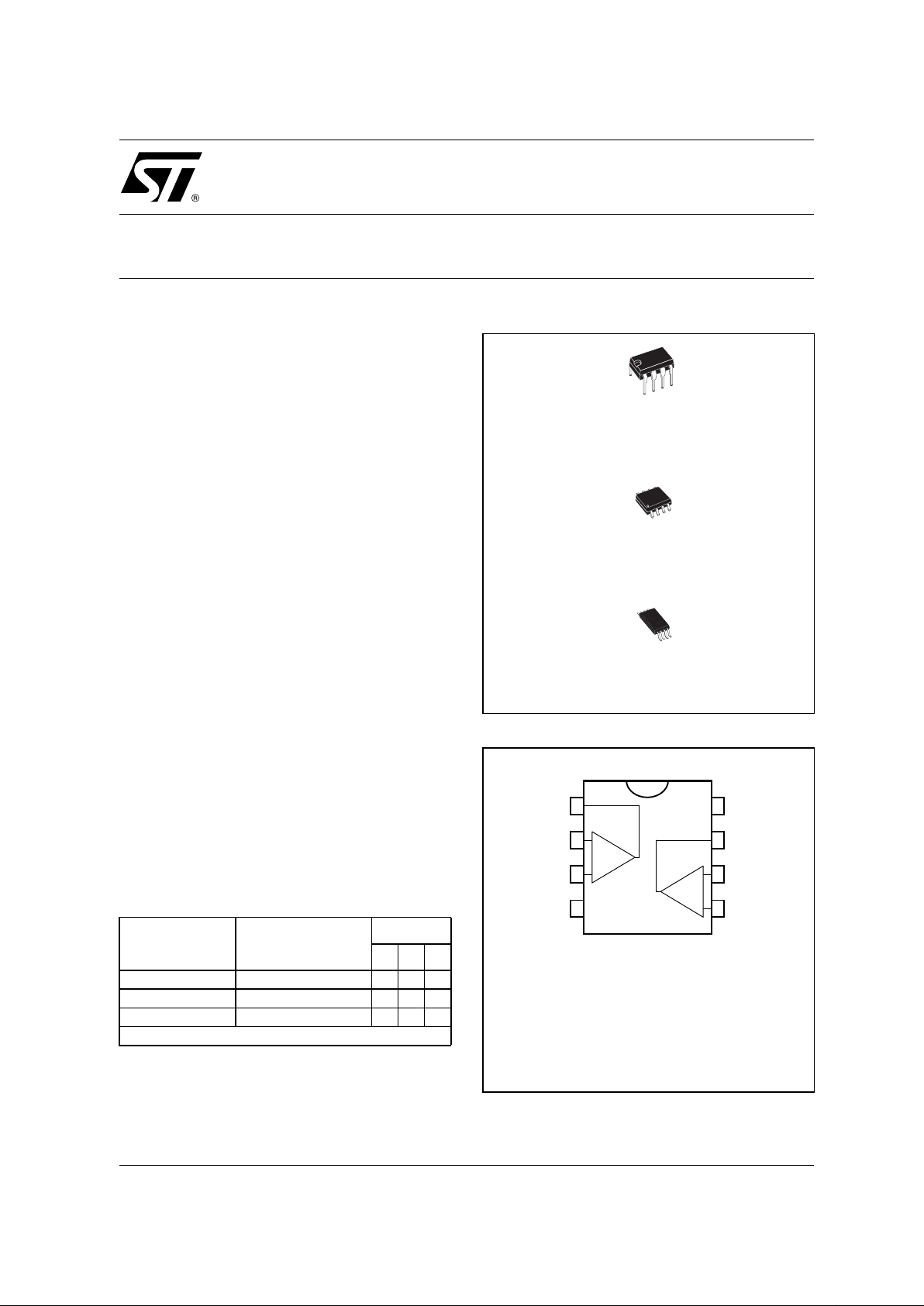
ORDER CODE
N = Dual in Line Package (DIP)
D = Small Outline Package (SO) - also available in Tape & Reel (DT)
P = Thin Shrink Small Outline Package (TSSOP) - only available
in Tape & Reel (PT)
PIN CONNECTIONS (top view)
Part Number Temperature Range
Package
NDP
TS27L2C/AC/BC 0°C, +70°C
•••
TS27L2I/AI/BI -40°C, +125°C
•••
TS27L2M/AM/BM -55°C, +125°C
•••
Example : TS27L2ACN
N
DIP8
(Plastic Package)
D
SO8
(Plastic Micropackage)
P
TSSOP8
(Thin Shrink Small Outline Package)
1
2
3
45
6
7
8
CC
+
-
-
+
-
+
CC
1 - Output 1
2 - Inverting Input 1
3 - Non-inverting Input 1
4 - V
5 - Non-inverting Input 2
6 - Inverting Input 2
7 - Output 2
8 - V
TS27L2C,I,M
PRECISION VERY LOW POWER
CMOS DUAL OPERATIONAL AMPLIFIERS
November 2001
Page 2
TS27L2C,I,M
2/9
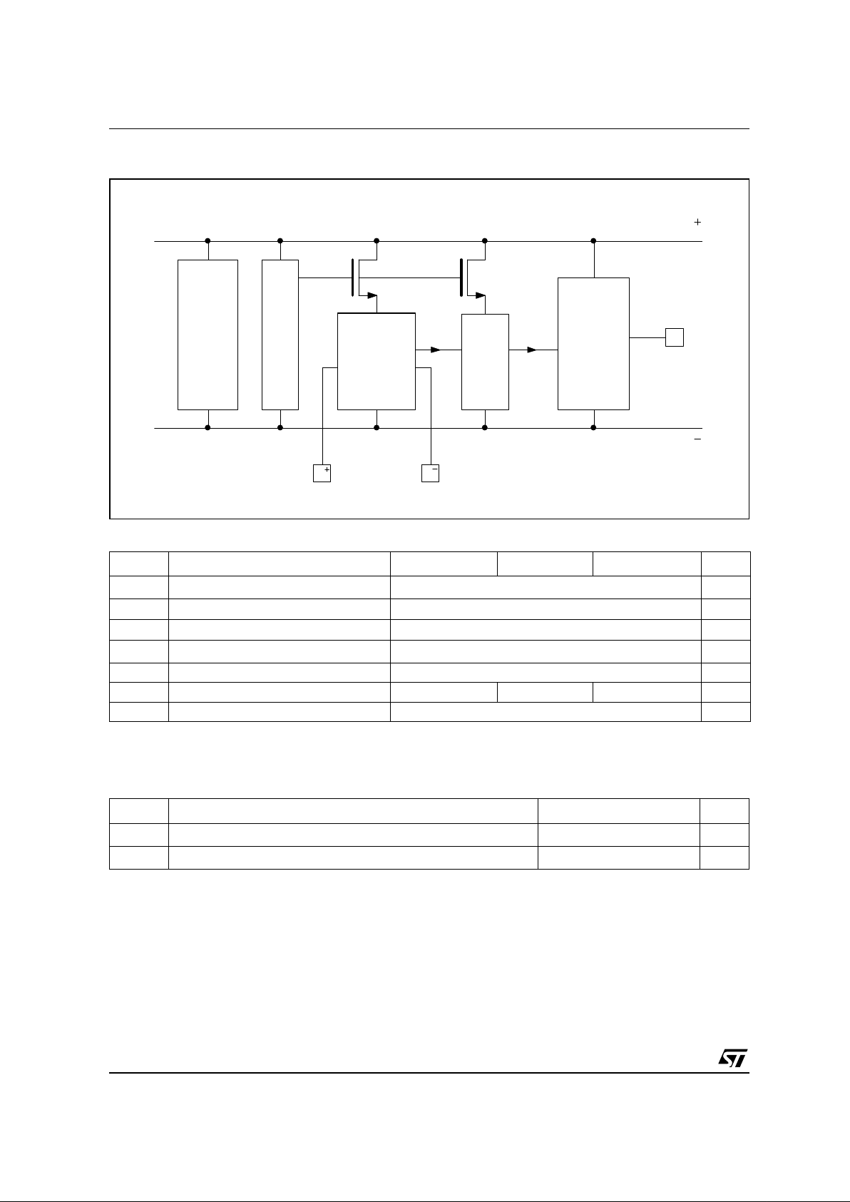
BLOCK DIAGRAM
ABSOLUTE MAXIMUM RATINGS
OPERATING CONDITIONS
E
E
Input
differential
Second
stage
Output
stage
Output
CC
V
CC
V
Current
source
x I
Symbol Parameter TS27L2C/AC/BC TS27L2I/AI/B I TS27L2M/AM/BM Unit
V
CC
+
Supply Voltage
1)
18 V
V
id Differential Input Voltage
2)
±18 V
V
i
Input Voltage
3)
-0.3 to 18 V
I
o
Output Current for V
CC
+
≥ 15V
±30 mA
I
in
Input Current ±5 mA
T
oper
Operating Free-Air Temperature Range 0 to +70 -40 to +125 -55 to +125 °C
T
stg
Storage Temperature Range -65 to +150 °C
1. All values, except differential voltage are with respect to network ground terminal.
2. Dif ferential vol tages are the non-invertin g i nput terminal w ith respect to the i nverting inpu t terminal.
3. The magnitude of the in put and the output voltages must never exceed the magnitude of the positive supply voltage.
Symbol Parameter Value Unit
V
CC
+
Supply Voltage 3 to 16 V
V
icm
Common Mode Input Voltage Range
0 to V
CC
+
- 1.5
V
Page 3
TS27L2C,I,M
3/9
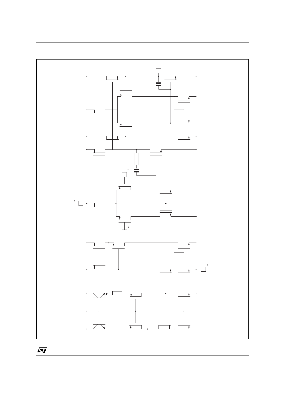
SCHEMATIC DIAGRAM (for 1/2 TS27L2)
T
T
25
2
T
17 18
R
T
20
T
21
T
T
23
22
Input
Output
T
24
T
19
V
CC
V
CC
T
26
T
27
T
28
T
29
Input
T
3
T
4
T
5
T
2
T
1
R1
C1
T
7
T
6
T
8
T
9
T
13
T
14
T
11
T
12
T
10
T
16
T
15
Page 4

TS27L2C,I,M
4/9
ELECTRICAL CHARACTERISTICS
V
CC
+
= +10V, V
CC
-
= 0V, T
amb
= +25°C (unless otherwise specified)
Symbol Parameter
TS27L2C/AC/BC
TS27L2I/AI/BI
TS27L2M/AM/BM
Unit
Min. Typ. Max. Min. Typ. Max.
V
io
Input Offset Voltage
V
O
= 1.4V, Vic = 0V TS27L2C/I/M
TS27L2AC/AI/AM
TS27L2B/C/I/M
T
min
≤ T
amb
≤ T
max
TS27L2C/I/M
TS27L2AC/AI/AM
TS27L2B/C/I/M
1.1
0.9
0.25
10
5
2
12
6.5
3
1.1
0.9
0.25
10
5
2
12
6.5
3.5
mV
DV
io
Input Offset Voltage Drift 2 2 µV/°C
I
io
Input Offset Current note
1)
Vic = 5V, VO = 5V
T
min
≤ T
amb
≤ T
max
1. Maximum values including unavoidable inaccuracies of the industrial test.
1
100
1
200
pA
I
ib
Input Bias Current - see note 1
Vic = 5V, VO = 5V
T
min
≤ T
amb
≤ T
max
1
150
1
300
pA
V
OH
High Level Output Voltage
V
id
= 100mV, RL = 1M
Ω
T
min
≤ T
amb
≤ T
max
8.8
8.7
98.8
8.6
9V
V
OL
Low Level Output Voltage
V
id
= -100mV
50 50
mV
A
vd
Large Signal Voltage Gain
V
iC
= 5V, RL = 1M
Ω,
Vo = 1V to 6V
T
min
≤ T
amb
≤ T
max
6045100 6040100 V/mV
GBP
Gain Bandwidth Product
A
v
= 40dB, RL = 1M
Ω,
CL = 100pF, fin = 100kHz
0.1 0.1
MHz
CMR
Common Mode Rejection Ratio
V
iC
= 1V to 7.4V, Vo = 1.4V
65 80 65 80
dB
SVR
Supply Voltage Rejection Ratio
V
CC
+
= 5V to 10V, Vo = 1.4V
60 80 60 80
dB
I
CC
Supply Current (per amplifier)
A
v
= 1, no load, Vo = 5V
T
min
≤ T
amb
≤ T
max
10 15
17
10 15
18
µA
I
o
Output Short Circuit Current
V
o
= 0V, Vid = 100mV
60 60
mA
I
sink
Output Sink Current
V
o
= VCC, Vid = -100mV
45 45
mA
SR
Slew Rate at Unity Gain
R
L
= 1MΩ, CL = 100pF, Vi = 3 to 7V
0.04 0.04
V/µs
φ
m
Phase Margin at Unity Gain
A
v
= 40dB, RL = 1MΩ, CL = 100pF
45 45
Degrees
K
OV
Overshoot Factor 30 30 %
e
n
Equivalent Input Noise Voltage
f = 1kHz, R
s
= 100
Ω
68 68
V
o1/Vo2
Channel Separation 120 120 dB
nV
Hz
----------- -
Page 5

TS27L2C,I,M
5/9
TYPICAL CHARACTERISTICS
Figure 1 : Supply Cur r en t ( e ac h am p li fi e r) versu s
Supply Voltage
Figure 2 : Input Bias Current versus Free Air
Temperature
Figure 3a : High Level Output Voltage versus
High Level Output Current
Figure 3b : High Level Output Voltage versus
High Level Output Current
Figure 4a : Low Level Output Voltage versus Low
Level Output Current
Figure 4b : Low Level Output Voltage versus Low
Level Output Current
CC
SUPPLY VOLTAGE, V (V)
CC
amb
V
OCC
°
0481216
20
µ
SUPPLY CURRENT, I ( A)
T=25C
A=1
V=V /2
15
10
5
25 50 75 100 125
amb
INPUT BIAS CURRENT, I (pA)
IB
TEMPERATURE,T ( C)
°
V = 10V
V=5V
CC
i
100
10
1
5
4
3
2
1
0
-10 -8 -6 -4 -2 0
OH
OUTPUT CURRENT,I (mA)
OUTPUT VO LTAGE, V (V)
OH
amb
id
T = 25 C
V = 100mV
°
V=5V
V=3V
CC
CC
20
16
12
8
4
0
-50 -40 -30 -20 -10 0
amb
id
°
T = 25 C
V = 100mV
V = 16V
CC
CC
V = 10V
OUTPUT CURRENT,I (mA)
OH
OH
OUTPUT VOL T AG E, V (V)
1.0
0.8
0.6
0.4
0.2
amb
ic
id
T=25°C
V = 0.5V
V = -100mV
V=3V
V=5V
CC
CC
OL
OUTPUT VO LTAGE, V
(V)
0123
OUTPUT CURRENT, I (mA)
OL
0 4 8121620
OUTPUT VOLTAGE, V (V)
OL
amb
id
i
T = 25°C
V=0.5V
V = -100mV
CC
V=10V
CC
V=16V
OUTPUT CURRENT, I (mA)
OL
3
2
1
Page 6

TS27L2C,I,M
6/9
Figure 5 : Open Loop Frequency Response and
Phase Shift
Figure 6 : Gain Bandwidth Product versus Supply
Voltage
Figure 7 : Phase Margin versus Supply Voltage
Figure 8 : Phase Margin versu s Capa cit i ve Load
Figure 9 : Slew Rate versus Supply Voltage
Figure 10 : Input Voltage Noise versus
Frequency
50
40
30
20
10
0
-10
6
10
10
23
10
4
10
5
10
7
10
GAIN (dB)
PHASE (Degrees)
0
45
90
135
180
FREQUENCY, f (Hz)
T = 25°C
V=10V
R=1M
Ω
C = 100pF
A=100
amb
CC
L
L
VCL
PHASE
GAIN
Phase
Margin
Gain
Bandwidth
Product
+
0481216
GAIN BANDW. PROD., GBP (MHz)
amb
L
L
V
T = 25°C
R=1M
Ω
C = 100pF
A=1
SUPPLY VOLTAGE, V (V)
CC
120
100
80
60
40
60
04 8 1216
SUPPLY VOLTAGE, V (V)
CC
amb
L
L
T=25°C
R=1M
C = 100pF
A=1
V
PHASE M ARGIN, m (Degrees)
φ
50
40
30
Ω
80
70
60
50
40
L
CAPACITANCE, C (pF)
PHASE MARGIN, m (Degrees)
φ
200
80
100
6040
T=25°C
R=1M
Ω
A=1
V=10V
amb
L
V
CC
0.05
0.04
0.03
0.02
4 6 8 10 12 14 16
SUPPLY VOLTAGE, V (V)
CC
SLEW RATES, SR (V/
µ
s)
amb
L
L
T=25°C
R=1M
Ω
C = 100pF
SR
SR
300
200
100
0
EQUIVALENT INPUT NO ISE
VOLTAGE (nV/VHz)
110
100
1000
FREQUENCY (Hz)
= 10V
=25°C
T
amb
V
CC
=100
Ω
R
S
Page 7

TS27L2C,I,M
7/9
PACKAGE MECHANICAL DATA
8 PINS - PLASTIC DIP
Dim.
Millimeters Inches
Min. Typ. Max. Min. Typ. Max.
A 3.32 0.131
a1 0.51 0.020
B 1.15 1.65 0.045 0.065
b 0.356 0.55 0.014 0.022
b1 0.204 0.304 0.008 0.012
D 10.92 0.430
E 7.95 9.75 0.313 0.384
e 2.54 0.100
e3 7.62 0.300
e4 7.62 0.300
F 6.6 0260
i 5.08 0.200
L 3.18 3.81 0.125 0.150
Z 1.52 0.060
Page 8

TS27L2C,I,M
8/9
PACKAGE MECHANICAL DATA
8 PINS - PLASTIC MICROPACKAGE (SO)
Dim.
Millimeters Inches
Min. Typ. Max. Min. Typ. Max.
A 1.75 0.069
a1 0.1 0.25 0.004 0.010
a2 1.65 0.065
a3 0.65 0.85 0.026 0.033
b 0.35 0.48 0.014 0.019
b1 0.19 0.25 0.007 0.010
C 0.25 0.5 0.010 0.020
c1 45° (typ.)
D 4.8 5.0 0.189 0.197
E 5.8 6.2 0.228 0.244
e 1.27 0.050
e3 3.81 0.150
F 3.8 4.0 0.150 0.157
L 0.4 1.27 0.016 0.050
M 0.6 0.024
S 8° (max.)
b
e3
A
a2
s
L
C
E
c1
a3
b1
a1
D
M
8
5
1
4
F
Page 9

TS27L2C,I,M
9/9
PACKAGE MECHANICAL DATA
8 PINS - THIN SHRINK SMALL OUTLIN E PAC KAGE (TSSOP)
Dim.
Millimeters Inches
Min. Typ. Max. Min. Typ. Max.
A 1.20 0.05
A1 0.05 0.15 0.01 0.006
A2 0.80 1.00 1.05 0.031 0.039 0.041
b 0.19 0.30 0.007 0.15
c 0.09 0.20 0.003 0.012
D 2.90 3.00 3.10 0.114 0.118 0.122
E 6.40 0.252
E1 4.30 4.40 4.50 0.169 0.173 0.177
e 0.65 0.025
k 0° 8° 0° 8°
l 0.50 0.60 0.75 0.09 0.0236 0.030
L 0.45 0.600 0.75 0.018 0.024 0.030
L1 1.000 0.039
C
L
14
8
5
L1
c
0.25mm
.010 inch
GAGE PLANE
E1
k
L
L1
E
SEATING
PLANE
A
A2
D
A1
b
5
8
4
1
PIN 1 IDENTIFICATION
e
Information furnished is beli eved to be accurate and reliable. However, STMicroe lectronics assumes no responsibility for the
consequences of use of such information nor for any infringement of patents or other rights of third parties which may result from
its use. No licens e is granted by implication or otherwise under any patent or patent rig hts of STMicroelectronics. Specifications
mentioned in this publication ar e subject to change without notice. This publication supersedes and replaces all information
previously supplied. S TMicroelectronics products are not authorized for use as critica l components in life suppo rt devices or
systems without express written approval of STMicroelectronics.
© The ST logo is a registered trademark of STMicroelectronics
© 2001 STM i cr o electronics - Printed in Italy - All Righ ts Reserved
STMicr oelectronics GROUP OF COMPANI E S
Australi a - Brazil - Can ada - China - Finland - France - Germany - Hon g Kong - India - Israel - Italy - Japan - Malaysi a
Malta - Mor occo - Singapore - Spain - Sweden - Switzerl and - United Kingdom - Unit ed States
© http://www.st.com
 Loading...