

Datasheet TS27L2IN, TS27L2ID, TS27L2I, TS27L2CN, TS27L2CD Datasheet (SGS Thomson Microelectronics)
...Page 1
TS27L2C,I,M
LOW POWER CMOS
DUALOPERATIONAL AMPLIFIERS
June 1998
.ULTRALOWCONSUMPTION: 10µA/op
.OUTPUT VOLTAGE CAN SWING TO
GROUND
.EXCELLENTPHASE MARGINON
CAPACITIVELOADS
.STABLEANDLOW OFFSETVOLTAGE
.THREEINPUT OFFSETVOLTAGE
SELECTIONS
1
2
3
45
6
7
8
CC
+
-
-
+
-
+
CC
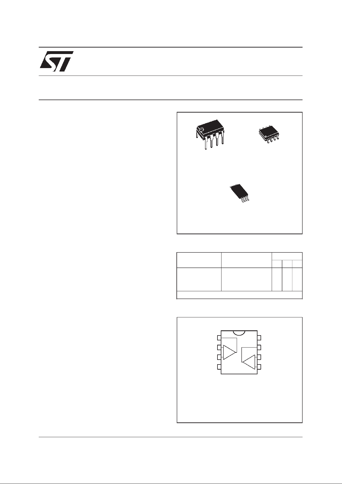
1 - Output 1
2 - InvertingInput1
3 - Non-invertingInput 1
4-V
5 - Non-invertingInput 2
6 - InvertingInput2
7 - Output 2
8-V
PIN CONNECTI O NS (t o p v iew)
N
DIP8
(PlasticPackage)
D
SO8
(PlasticMicropackage)
DESC RIP TI ON
The TS272seriesare low cost, lowpowerdualoperationalamplifiers designedtooperatewith single
or dual supplies. These operationalamplifiers use
the SGS-THOMSONsilicongateCMOSprocessallowing an excellent consumption-speed ratio.
Theseseries areideallysuitedforlowconsumption
applications.
Threepowerconsumptionsareavailableallowingto
have alwaysthe bestconsumption-speedratio :
l ICC = 10mA/amp.: TS27L2 (verylow power)
l ICC=150mA/amp.: TS27M2(lowpower)
l ICC=1mA/amp.: TS272 (highspeed)
TheseCMOSamplifiersofferveryhighinputimpedance and extremelylow input currents.The major
advantageversusJFETdevicesistheverylowinput
currentsdrift with temperature(see figure2).
ORDER CODES
Part Number
Temperature
Range
Package
NDP
TS27L2C/AC/BC 0
o
C, +70oC ●●●
TS27L2I/AI/BI -40oC, +125oC ●●●
TS27L2M/AM/BM -55oC, +125oC ●●●
Example : TS27L2ACN
P
TSSOP8
(Thin ShrinkSmall Outline Package)
1/9
Page 2
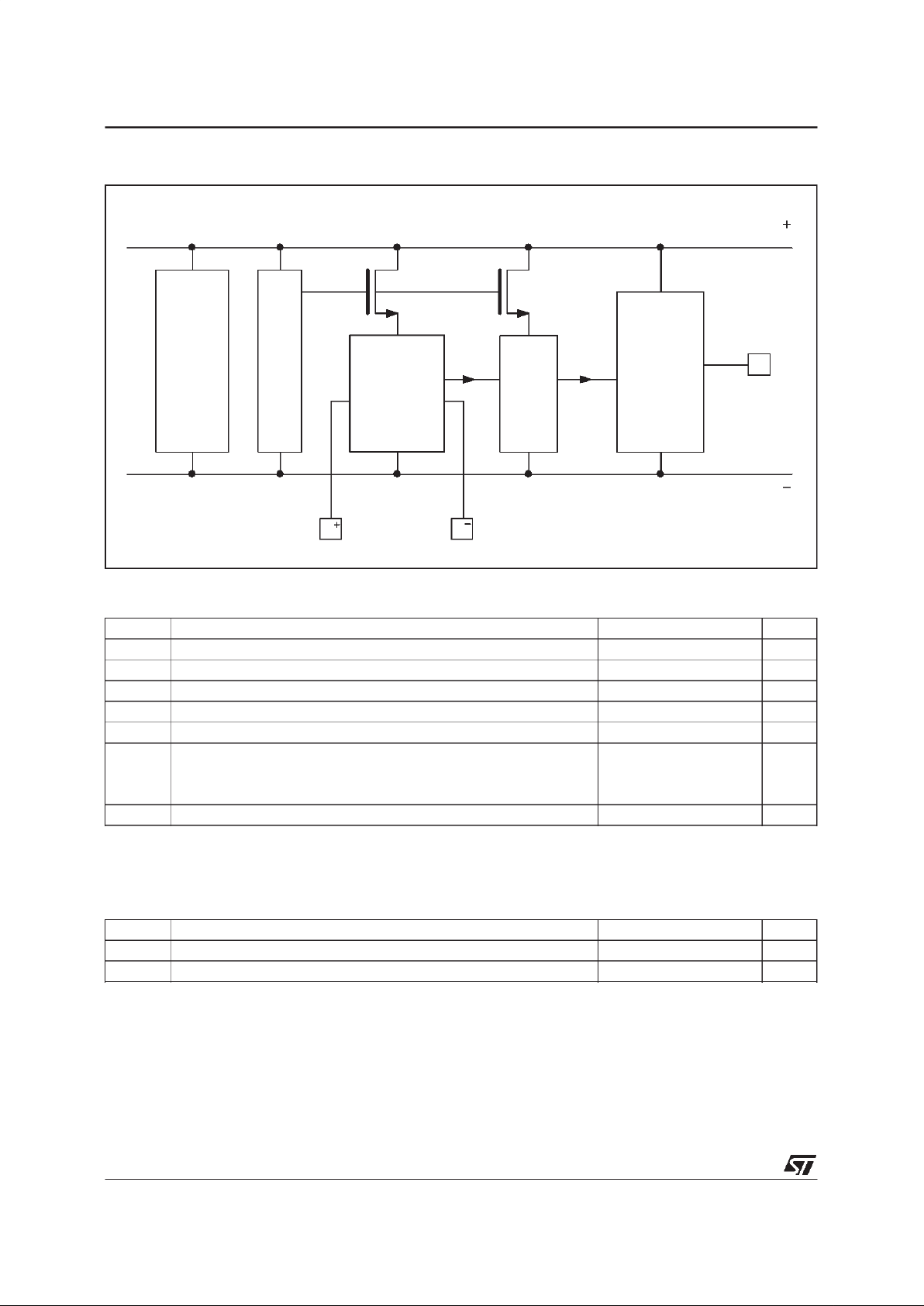
E E
Input
differential
Second
stage
Output
stage
Output
CC
V
CC
V
Current
source
xI
BLOCK DIAGRAM
MAXIMUM RATINGS
Symbol Parameter Value Unit
V
CC
+
Supply Voltage - (note 1) 18 V
V
id
Differential Input Voltage - (note 2) ±18 V
V
i
Input Voltage - (note 3) -0.3 to 18 V
I
O
Output Current for V
CC
+
≥ 15V ±30 mA
I
in
Input Current ±5mA
T
oper
Operating Free-Air Temperature Range
TS27L2C/AC/BC
TS27L2I/AI/BI
TS27L2M/AM/BM
0 to +70
-40 to +125
-55 to +125
o
C
T
stg
Storage Temperature Range -65 to +150
o
C
Notes : 1.All voltage values, exc ept differential voltage, ar e with resp ec t t o network ground t er minal.
2.Di f ferential voltages are at the non- inverting input t ermi nal wi t h respect t o the invert i ng input term inal.
3.The ma gni tude of the input and the outp ut vol t ages must never exceed the magnitud e of the pos itive supply volt age.
OPERATING CONDITIONS
Symbol Parameter Value Unit
V
CC
+
Supply Voltage 3 to 16 V
V
icm
Common Mode Input Voltage Range 0 to V
CC
+
- 1.5 V
TS27L2C,I,M
2/9
Page 3
T
T
25
2
T
17 18
R
T
20
T
21
T
T
23
22
Input
Output
T
24
T
19
V
CC
V
CC
T
26
T
27
T
28
T
29
Input
T
3
T
4
T
5
T
2
T
1
R1
C1
T
7
T
6
T
8
T
9
T
13
T
14
T
11
T
12
T
10
T
16
T
15
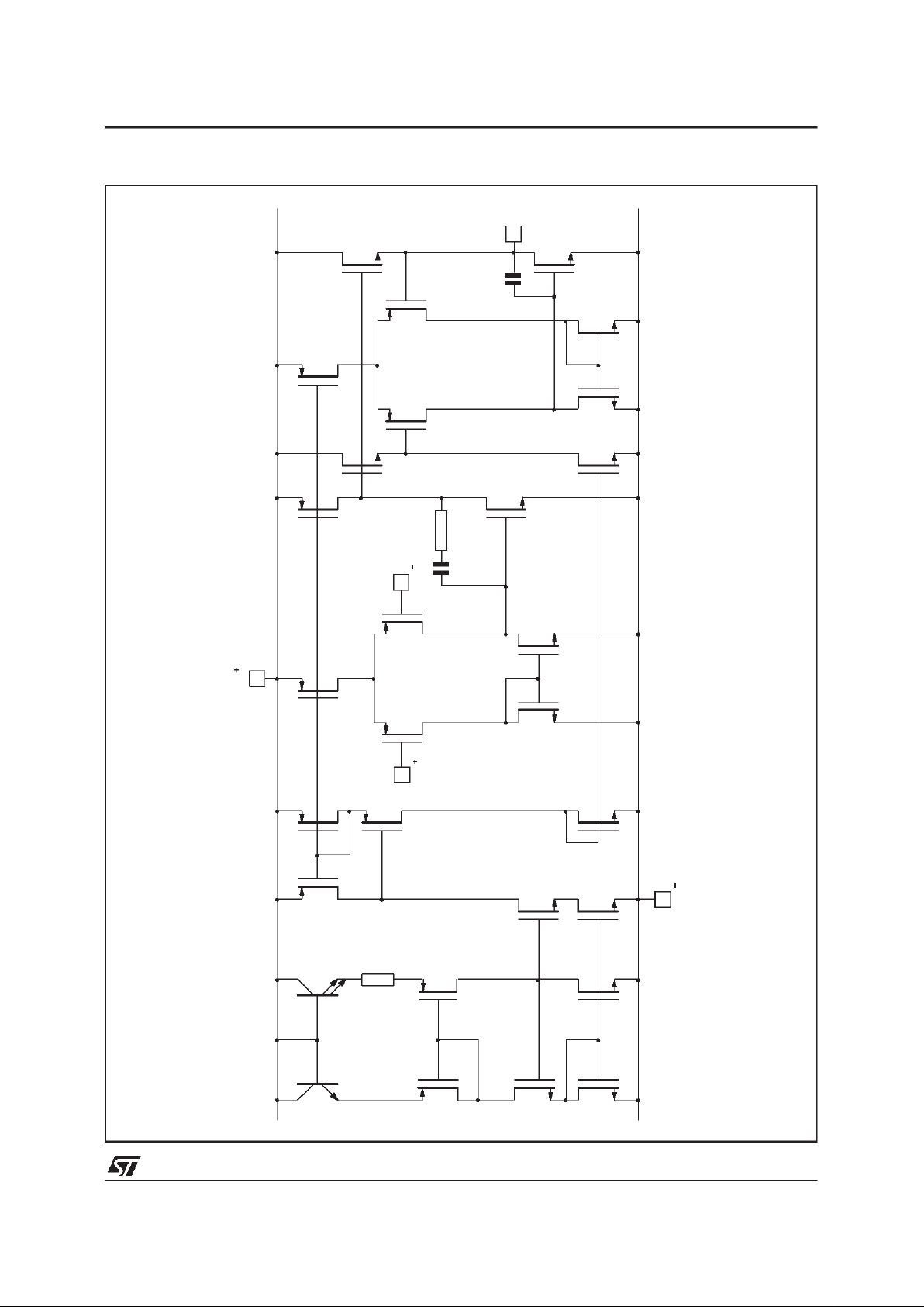
SCHE MATIC DIAGRAM (for 1 /2 TS27L2)
TS27L2C,I,M
3/9
Page 4

ELECTRICAL CHARACTERISTICS
V
CC
+
= +10V, V
CC
-
= 0V, T
amb
=25oC (unless otherwise specified)
Symbol Parameter
TS27L2C/AC/BC
TS27L2I/AI/BI
TS27L2M/AM/BM
Unit
Min. Typ. Max. Min. Typ. Max.
V
io
Input Offset Voltage
V
O
= 1.4V, Vic= 0V TS27L2C/I/M
TS27L2AC/AI/AM
TS27L2BC/BI/BM
T
min
. ≤ T
amb
≤ T
max.
TS27L2C/I/M
TS27L2AC/AI/AM
TS27L2BC/BI/BM
1.1
0.9
0.25
10
5
2
12
6.5
3
1.1
0.9
0.25
10
5
2
12
6.5
3.5
mV
DV
io
Input Offset Voltage Drift 0.7 0.7 µV/oC
I
io
Input Offset Current - (note 1)
V
ic
= 5V, Vo=5V
T
min
. ≤ T
amb
≤ T
max.
1
100
1
200
pA
I
ib
Input Bias Current - (note 1)
V
ic
= 5V, Vo=5V
T
min
. ≤ T
amb
≤ T
max.
1
150
1
300
pA
V
OH
High Level Output Voltage
V
id
= 100mV, RL=1MΩ
T
min
. ≤ T
amb
≤ T
max.
8.8
8.7
9 8.8
8.6
9
V
V
OL
Low Level Output Voltage
V
id
= -100mV 50 50
mV
A
vd
Large Signal Voltage Gain
V
o
= 1V to 6V, RL=1MΩ,Vic=5V
T
min
. ≤ T
amb
≤ T
max.
6045100 6040100
V/mV
GBP Gain Bandwidth Product
Av= 40dB, RL=1MΩ,CL= 100pF
f
in
= 100kHz
0.1 0.1
MHz
CMR Common Mode Rejection Ratio
V
o
= 1.4V, Vic= 1V to 7.4V 65 80 65 80
dB
SVR Supply Voltage Rejection Ratio
V
CC
+
= 5V to 10V ,Vo= 1.4V 60 80 60 80
dB
I
CC
Supply Current (per amplifier)
A
v
= 1, no load, Vo=5V
T
min
. ≤ T
amb
≤ T
max.
10 15
17
10 15
18
µA
I
o
Output Short Circuit Current
V
id
= 100mV, Vo=0V 60 60
mA
I
sink
Output Sink Current
V
id
= -100mV, Vo=V
CC
45 45
mA
SR Slew-Rate at Unity Gain
R
L
=1MΩ,CL= 100pF, Vi= 3 to 7V 0.04 0.04
V/µs
∅m Phase Margin at Unity Gain
A
v
= 40dB, RL=1MΩ,CL= 100pF 45 45
Degrees
K
ov
Overshoot Factor 30 30 %
e
n
Equivalent Input Noise Voltage
f = 1kHz, R
S
= 100Ω 68 68
nV
√Hz
V
O1/VO2
Channel Separation 120 120 dB
Note : 1.Max imum values in cluding unavoidable inaccur ac i es of the industrial test .
TS27L2C,I,M
4/9
Page 5

TYP ICAL CHARACTERI STICS
CC
SUP PLYVOLTAGE, V (V)
CC
AMB
V
OCC
0481216
20
µ
SUPPLY CURRENT, I ( A)
T=25C
A=1
V=V /2
15
10
5
Figure 1 : Supply Current (each amplifier)
versus Supply Voltage
5
4
3
2
1
0
-10 -8 -6 -4 -2 0
OHOUTPUT CURRE NT, I (mA)
OUTPUT VOLTAGE, V (V)
OH
AMB
ID
T = 25 C
V = 100mV
°
V=5V
V=3V
CC
CC
Figure 3a :High Level Output Voltage versus
High Level Output Current
20
16
12
8
4
0
-50 -40 -30 -20 -10 0
AMB
ID
°
T = 25 C
V = 100mV
V = 16V
CC
CC
V = 10V
OUTPUT CURRENT, I (mA)
OH
OH
OUTPUT VOLTAGE, V (V)
Figure 3b :High Level Output Voltage versus
High Level Output Current
1.0
0.8
0.6
0.4
0.2
amb
ic
id
T=25
C
V = 0.5V
V = -100mV
V=3V
V=5V
CC
CC
OL
OUTPUT VOLTAGE, V (V)
0123
OUTPUT CURRENT, I (mA)
OL
Figure 3a :Low Level Output Voltage versus
Low Level Output Current
048121620
OUTPUT VOLTAGE, V (V)
OL
amb
id
i
T=25 C
V = 0.5V
V = -100mV
CC
V=10V
CC
V = 16V
OUTPUT CURRENT, I (mA)
OL
3
2
1
Figure 3b :Low Level Output Voltage versus
Low Level Output Current
25 50 75 100 125
AMB
INPUT BIAS CURRENT, I (pA)
IB
TEMPERATURE, T ( C)
°
V = 10V
V=5V
CC
i
100
10
1
Figure 2 : Input Bias Current versus Free Air
Temperature
TS27L2C,I,M
5/9
Page 6

TYP ICAL CHARACTERI STICS (continued)
60
04 8 1216
SUPPLYVOLTAGE, V (V)
CC
amb
L
L
T=25
C
R=1M
Ω
C = 10 0pF
A=1
V
PHASE MARGIN, m (Degrees)
φ
50
40
30
Figure 7 : Phase Margin versusSupply Voltage
80
70
60
50
40
L
CAPACITANCE, C (pF)
PHASE MARGIN, m (Degrees)
φ
200
80
100
6040
T=25 C
R=1M
Ω
A=1
V=10V
amb
L
V
CC
Figure 8 : Phase Margin versus CapacitiveLoad
50
40
30
20
10
0
-10
6
10
10
23
10
4
10
5
10
7
10
GAIN (dB)
PHASE (Degrees)
0
45
90
135
180
FREQUENCY, f (Hz)
T=25
C
V=10V
R=1M
Ω
C = 100pF
A=100
amb
CC
L
L
VCL
PHASE
GAIN
Phase
Margin
Gain
Bandwidth
Product
+
Figure 5 : Open Loop Frequency Response and
Phase Shift
0481216
GAIN BANDW. PROD., GBP (MHz)
amb
L
L
V
T=25 C
R=1M
Ω
C = 100p F
A=1
SUPPLYVOLTAGE, V (V)
CC
120
100
80
60
40
Figure 6 : Gain BandwidthProduct versus
Supply Voltage
0.05
0.04
0.03
0.02
4 6 8 10 12 14 16
SUPPLY VOLTAGE, V (V)
CC
SLEW RATES, SR (V/
µ
s)
amb
L
L
T=25
C
R=1M
Ω
C = 10 0p F
SR
SR
Figure 9 : Slew Rate versus Supply Voltage
300
200
100
0
EQUIVALENT INPUT NOISE
VOLTAGE (nV/VHz)
110
100
1000
FREQUENCY(Hz)
=10V
=25 CT
amb
V
CC
= 100
Ω
R
S
Figure 10 : Input Voltage Noise versus
Frequency
TS27L2C,I,M
6/9
Page 7

PM-DIP8.EPS
PACKAG E MECHANICAL DATA
8 PINS - PLASTIC DIP
Dimensions
Millimeters Inches
Min. Typ. Max. Min. Typ. Max.
A 3.32 0.131
a1 0.51 0.020
B 1.15 1.65 0.045 0.065
b 0.356 0.55 0.014 0.022
b1 0.204 0.304 0.008 0.012
D 10.92 0.430
E 7.95 9.75 0.313 0.384
e 2.54 0.100
e3 7.62 0.300
e4 7.62 0.300
F 6.6 0260
i 5.08 0.200
L 3.18 3.81 0.125 0.150
Z 1.52 0.060
DIP8.TBL
TS27L2C,I,M
7/9
Page 8

PM-SO8.EPS
PACKAG E MECHANICAL DATA
8 PINS - PLASTIC MICROPACKAGE (SO)
Dimensions
Millimeters Inches
Min. Typ. Max. Min. Typ. Max.
A 1.75 0.069
a1 0.1 0.25 0.004 0.010
a2 1.65 0.065
a3 0.65 0.85 0.026 0.033
b 0.35 0.48 0.014 0.019
b1 0.19 0.25 0.007 0.010
C 0.25 0.5 0.010 0.020
c1 45
o
(typ.)
D 4.8 5.0 0.189 0.197
E 5.8 6.2 0.228 0.244
e 1.27 0.050
e3 3.81 0.150
F 3.8 4.0 0.150 0.157
L 0.4 1.27 0.016 0.050
M 0.6 0.024
S8
o
(max.)
SO8.TBL
TS27L2C,I,M
8/9
Page 9

PACKAGE ME CHA NI CAL DATA
8 PINS - THIN SHRINK S M AL L OUTLI NE PACKAG E
Dim.
Millimeters Inches
Min. Typ. Max. Min. Typ. Max.
A 1.20 0.05
A1 0.05 0.15 0.01 0.006
A2 0.80 1.00 1.05 0.031 0.039 0.041
b 0.19 0.30 0.007 0.15
c 0.09 0.20 0.003 0.012
D 2.90 3.00 3.10 0.114 0.118 0.122
E 6.40 0.252
E1 4.30 4.40 4.50 0.169 0.173 0.177
e 0.65 0.025
k0
o
8
o
0
o
8
o
l 0.50 0.60 0.75 0.09 0.0236 0.030
Information furnished is believed to be accurate and reliable. However, STMicroelectronics assumes no responsibility for the
consequences of use of such information nor for any infringement of patents or other rights of third parties which may result
from its use. No license is granted by implication or otherwise under any patent or patent rights of STMicroelectronics. Specifications mentioned in this publication are subject to change without notice. This publication supersedes and replaces all information previously supplied. STMicroelectronics products are not authorized for use as critical components in life support
devices or systems without express written approval of STMicroelectronics.
The ST logo is a trademark of STMicroelectronics
1998 STMicroelectronics – Printed in Italy – AllRights Reserved
STMicroelectronics GROUP OF COMPANIES
Australia - Brazil - Canada - China - France - Germany - Italy - Japan - Korea - Malaysia - Malta - Mexico - Morocco
The Netherlands - Singapore - Spain - Sweden - Switzerland - Taiwan - Thailand - United Kingdo m- U.S.A.
ORDERCODE :
TS27L2C,I,M
9/9
 Loading...