

Page 1
TR8 SERIES
SILICON TRIACS
l
8 A RMS, 70 A Peak
l
Glass Passivated Wafer
l
400 V to 800 V Off-State Voltage
l
Max IGT of 50 mA (Quadrants 1 - 3)
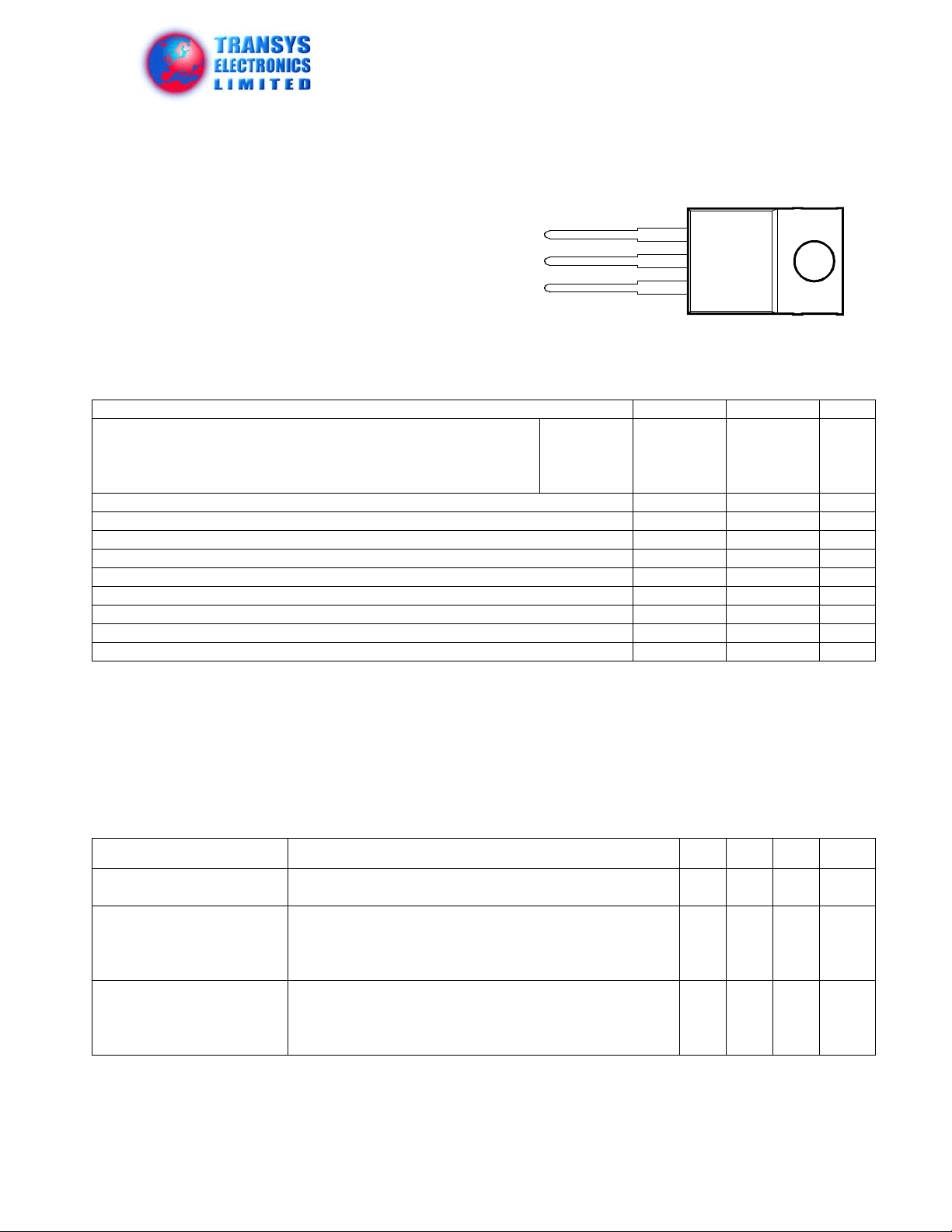
MT1
MT2
G
TO-220 PACKAGE
(TOP VIEW)
Pin 2 is in electrical contact with the mounting base.
1
2
3
absolute maximum ratings
over operating case temperature (unless otherwise noted
)
NOTES: 1. These values apply bidirectionally for any value of resistance between the gate and Main Terminal 1.
2. This value applies for 50-Hz full-sine-wave operation with resistive load. Above 85°C derate linearly to 110°C case temperature at
the rate of 320 mA/°C.
3. This value applies for one 50-Hz full-sine-wave when the device is operating at (or below) the rated value of on-state current.
Surge may be repeated after the device has returned to original thermal equilibrium. During the surge, gate control may be lost.
4. This value applies for one 50-Hz half-sine-wave when the device is operating at (or below) the rated value of on-state current.
Surge may be repeated after the device has returned to original thermal equilibrium. During the surge, gate control may be lost.
5. This value applies for a maximum averaging time of 20 ms.
RATING SYMBOL VALUE UNIT
Repetitive peak off-state voltage (see Note 1)
TR8-400-70
TR8-600-70
TR8-700-70
TR8-800-70
V
DRM
400
600
700
800
V
Full-cycle RMS on-state current at (or below) 85°C case temperature (see Note 2) I
T(RMS)
8
A
Peak on-state surge current full-sine-wave (see Note 3) I
TSM
70
A
Peak on-state surge current half-sine-wave (see Note 4) I
TSM
80 A
Peak gate current I
GM
±1 A
Peak gate power dissipation at (or below) 85°C case temperature (pulse width
£ 200 m s) P
GM
2.2 W
Average gate power dissipation at (or below) 85°C case temperature (see Note 5) P
G(AV)
0.9 W
Operating case temperature range T
C
-40 to +110 °C
Storage temperature range T
stg
-40 to +125 °C
Lead temperature 1.6 mm from case for 10 seconds T
L
230 °C
electrical characteristics at 25°C case temperature (unless otherwise noted)
PARAMETER TEST CONDITIONS
MIN TYP MAX
UNIT
I
DRM
Repetitive peak
off-state current
V
D
= rated V
DRM
IG = 0 TC = 110°C ±2 mA
I
GTM
Peak gate trigger
current
V
supply
= +12 V†
V
supply
= +12 V†
V
supply
= -12 V†
V
supply
= -12 V†
R
L
= 10 W
RL = 10 W
RL = 10 W
RL = 10 W
t
p(g)
> 20 m s
t
p(g)
> 20 m s
t
p(g)
> 20 m s
t
p(g)
> 20 m s
2
-12
-9
20
50
-50
-50
mA
V
GTM
Peak gate trigger
voltage
V
supply
= +12 V†
V
supply
= +12 V†
V
supply
= -12 V†
V
supply
= -12 V†
R
L
= 10 W
RL = 10 W
RL = 10 W
RL = 10 W
t
p(g)
> 20 m s
t
p(g)
> 20 m s
t
p(g)
> 20 m s
t
p(g)
> 20 m s
0.7
-0.8
-0.8
0.9
2
-2
-2
2
V
† All voltages are with respect to Main Terminal 1.
Page 2
TR8 SERIE
S
SILICON TRIACS
† All voltages are with respect to Main T
erminal 1
.
NOTES: 6. This parameter must be measured using pulse techniques, t
p
= £ 1 ms, duty cycle £ 2 %. Voltage-sensing contacts separate from
the current carrying contacts are located within 3.2 mm from the device body.
7. The triacs are triggered by a 15-V (open-circuit amplitude) pulse supplied by a generator with the following characteristics:
R
G
= 100 W , t
p(g)
= 20 m s, tr = £ 15 ns, f = 1 kHz.
V
TM
Peak on-state voltage ITM = ±12 A IG = 50 mA (see Note 6) ±1.6 ±2.1 V
I
H
Holding current
V
supply
= +12 V†
V
supply
= -12 V†
I
G
= 0
I
G
= 0
Init’ I
TM
= 100 mA
Init’ I
TM
= -100 mA
5
-9
30
-30
mA
I
L
Latching current
V
supply
= +12 V†
V
supply
= -12 V†
(see Note 7)
50
-50
mA
dv/dt
Critical rate of rise of
off-state voltage
V
DRM
= Rated V
DRMIG
= 0 TC = 110°C ±100 V/µs
dv/dt
(c)
Critical rise of commutation voltage
V
DRM
= Rated V
DRMITRM
= ±12 A TC = 85°C ±5 V/µs
thermal characteristics
PARAMETER MIN TYP MAX UNIT
R
q JC
Junction to case thermal resistance 1.8 °C/W
R
q JA
Junction to free air thermal resistance 62.5 °C/W
electrical characteristics at 25°C case temperature (unless otherwise noted) (continued)
PARAMETER TEST CONDITIONS
MIN TYP MAX
UNIT
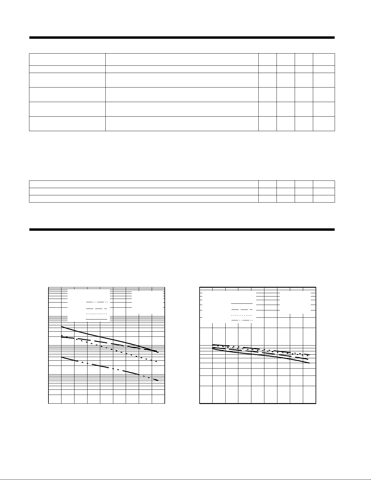
TYPICAL CHARACTERISTICS
Figure 1. Figure 2.
GATE TRIGGER CURRENT
TC - Case Temperature - °C
-60 -40 -20 0 20 40 60 80 100 120
I
GT
- Gate Trigger Current - mA
0·1
1
10
100
1000
CASE TEMPERATURE
vs
VAA = ± 12 V
R
L
= 10 W
W
t
p(g)
= 20 µs
V
supply IGTM
+ +
+ -
- -
- +
GATE TRIGGER VOLTAGE
TC - Case Temperature - °C
-60 -40 -20 0 20 40 60 80 100 120
V
GT
- Gate Trigger Voltage - V
0·1
1
10
CASE TEMPERATURE
vs
V
suppl y IGTM
+ +
+ -
- -
- +
VAA = ± 12 V
R
L
= 10 WW
t
p(g)
= 20 µs
Page 3

TR8 SERIES
SILICON TRIACS
TYPICAL CHARACTERISTICS
Figure 3. Figure 4.
Figure 5. Figure 6.
HOLDING CURRENT
TC - Case Temperature - °C
-60 -40 -20 0 20 40 60 80 100 120
I
H
- Holding Current - mA
0·1
1
10
100
1000
CASE TEMPERATURE
vs
V
suppl y
+
-
VAA = ± 12 V
IG = 0
Initiating I
T
M
= 100 mA
GATE FORWARD VOLTAGE
IGF - Gate Forward Current - A
0·0001 0·001 0·01 0·1 1
V
GF
- Gate Forward Voltage - V
0·01
0·1
1
10
GATE FORWARD CURRENT
vs
IA = 0
TC = 25 °C
QUADRANT 1
LATCHING CURRENT
TC - Case Temperature - °C
-60 -40 -20 0 20 40 60 80 100 120
I
L
- Latching Current - mA
1
10
100
1000
CASE TEMPERATURE
vs
VAA = ± 12 V
V
supply IGTM
+ +
+ -
- -
- +
SURGE ON-STATE CURRENT
Consecutive 50-Hz Half-Sine-Wave Cycles
1 10 100 1000
I
TSM
- Peak Full-Sine-Wave Current - A
1
10
100
C
YCLES OF CURRENT DURATION
vs
No Prior Device Conduction
Gate Contr ol Guaranteed
TC ££ 85 °C
Page 4

TR8 SERIE
S
SILICON TRIACS
TYPICAL CHARACTERISTICS
Figure 7. Figure 8.
PARAMETER MEASUREMENT INFORMATION
MAX RMS ON-STATE CURRENT
TC - Case Temperature - °C
0 25 50 75 100 125 150
I
T(RMS)
- Maximum On-State Current - A
0
1
2
3
4
5
6
7
8
9
10
CASE TEMPERATURE
vs
MAX AVERAGE POWER DISSIPATED
I
T(RMS)
- RMS On-State Current - A
0 2 4 6 8 10 12 14 16
P
(av)
- Maximum Average Power Dissipated - W
0
4
8
12
16
20
24
28
32
RMS ON-STATE CURRENT
vs
Conduction Angle = 360 °
Above 8 A rms
TJ = 110 °C
See I
TSM
Figure
V
AC
V
MT2
I
MT2
DUT
R
G
C1
R1
I
G
V
AC
I
MT2
V
MT2
I
G
I
TRM
dv/dt
10%
63%
L1
V
DRM
50 Hz
NOTE A: The gate-current pulse is furnished by a trigger circuit which presents essentially an open circuit between pulses. The pulse is timed
so that the off-state-voltage duration is approximately 800 µs.
Figure 9.
Page 5

TR8 SERIES
SILICON TRIACS
TO-220
3-pin plastic flange-mount package
This single-in-line package consists of a circuit mounted on a lead frame and encapsulated within a plastic
compound. The compound will withstand soldering temperature with no deformation, and circuit performance
characteristics will remain stable when operated in high humidity conditions. Leads require no additional
cleaning or processing when used in soldered assembly.
MECHANICAL DATA
TO220
ALL LINEAR DIMENSIONS IN MILLIMETERS
ø
1,23
1,32
4,20
4,70
1 2 3
0,97
0,61
see Note C
see Note B
10,0
10,4
2,54
2,95
6,0
6,6
14,55
15,90
12,7
14,1
3,5
6,1
1,07
1,70
2,34
2,74
4,88
5,28
3,71
3,96
0,41
0,64
2,40
2,90
VERSION 2 VERSION 1
NOTES: A. The centre pin is in electrical contact with the mounting tab.
B. Mounting tab corner profile according to package version.
C. Typical fixing hole centre stand off height according to package version.
Version 1, 18.0 mm. Version 2, 17.6 mm.
 Loading...