

Page 1

T R I Q U I N T S E M I C O N D U C T O R , I N C .
1
DATACOM
PRODUCTS
For additional information and latest specifications, see our website: www.triquint.com
TQ9501/9502
531/1063 Mbaud
Fibre Channel
Transmitter and
Receiver
Features
• Compliant with ANSI X3T11
Fibre Channel Standard
• Operates at 531.125 Mbaud
and 1.0625 Gigabaud
(1.25 Gigabaud max)
• Low power dissipation
(2.25 W, typical)
• Low jitter
• No external PLL components
• 10-bit TTL-compatible data bus
• Synchronous Data Bus Interface
•
Direct interface to TQ9303 ENDEC
• Single +5 V supply
• 48-pin MQuad package
TQ9501
Transmitter
2
TQ9303
ENDEC
TQ9502
Receiver
2
Data
10
Data
Data
32
Control
12
HOST
Optical Rx
or Copper
Interface
10
Optical Tx
or Copper
Interface
2
2
Fiber
Optic
Cable
Parity
4
Parity
4
Control
11
Data
32
Control
2
Control
2
2
TriQuint’s Fibre Channel transmitter (TQ9501) and receiver (TQ9502) are
part of the FC531/FC1063 (Fibre Channel 531 and 1063 Megabaud) chip
set. In addition to the transmitter and receiver, TriQuint offers the ENcoder/
DECoder (TQ9303 ENDEC). The TQ9501, TQ9502, TQ9303 and a gigabit
fiber optic module set provide a complete solution for Fibre Channel's FC0
and FC1 layers as well as partial support for the FC2 layer.
The TQ9501 and TQ9502 are designed in TriQuint's proprietary 0.7-micron
GaAs process, enabling the transmitter and receiver to run at higher speeds
and lower power than with conventional processes. The transmitter and
receiver data interface has been selected to be 10 bits in order to conserve
input/output power and to reduce pin count and package size. The transmitter performs the parallel-to-serial conversion and generates the internal
high-speed clock for the serial output. The receiver performs serial-toparallel conversion, recovers the clock and data from the serial input, and
detects the K28.5 character (Fibre Channel standard “SYNC” transmission
character).
The TQ9303 ENDEC implements 8b/10b encoding and decoding, ordered
set encoding and decoding, parity checking and generation, 32-bit CRC
checking and generation, and word synchronization as defined in the
Fibre Channel Physical and Signaling Interface Standard (FC-PH).
Fibre Channel provides a high-speed physical layer for Intelligent
Peripheral Interface (IPI) and Small Computer System Interface (SCSI)
upper-layer command sets, High-Performance Parallel Interface (HIPPI)
data link layer, and other user-defined command sets. Fibre Channel
replaces the SCSI, IPI and HIPPI physical interfaces with a higherspeed interface capable of driving longer distances.
Page 2
TQ9501/TQ9502
2
For additional information and latest specifications, see our website: www.triquint.com
Fibre Channel is optimized for predictable transfers of
large blocks of data, such as those used in file
transfers between processors (super computer,
mainframe, super-mini, etc.), storage systems (disk
and tape), and output-only devices such as laser
printers and raster scan graphics terminals.
The Fibre Channel protocol is implemented in
hardware, making it simple, efficient and robust. The
lower-level physical interface is decoupled from the
higher-level protocol allowing the Fibre Channel to be
configured with various topologies, including point-topoint, multi-drop bus, ring, and cross point switch.
Fibre Channel supports distances up to 10 Km at baud
rates of 132.8125 Mbaud to 1.0625 Gbaud. Copper
media such as Coax and STP (Shielded Twisted Pair)
are used for shorter distances while fiber optic cables
are used for longer distances.
Applications for the TQ9501 and TQ9502 include serial
SCSI, IPI, HIPPI, point-to-point serial communication,
ATM and other networking applications.
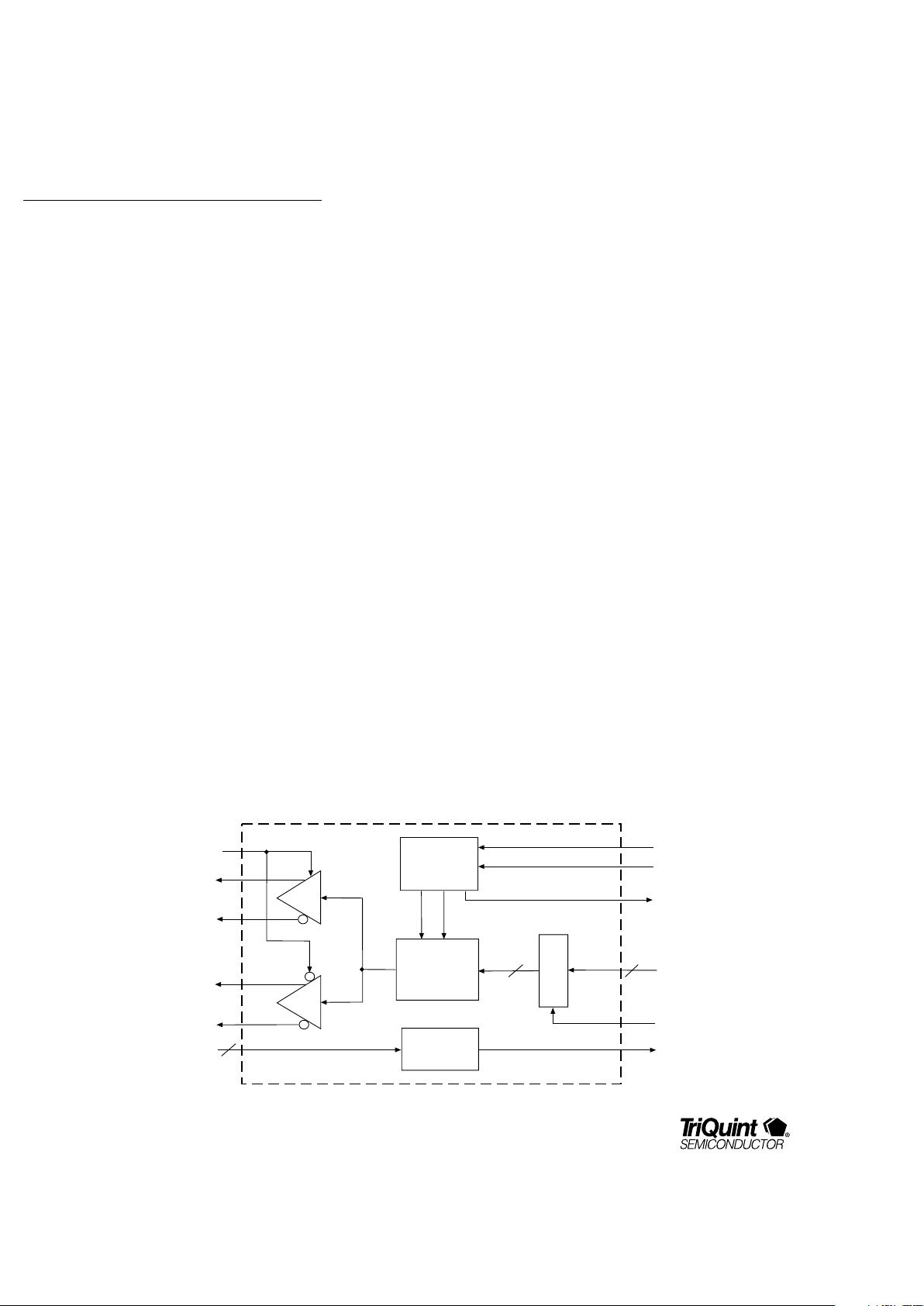
Functional Description – TQ9501 Transmitter
The TQ9501 serializes a 10-bit TTL input into a
differential PECL output. The TQ9501 is composed of
an input register, a parallel-to-serial converter, a PLL
clock generator, a differential output buffer and a PECLto-TTL translator, as illustrated in Figure 1.
The self-contained PLL (Phase-Locked Loop) clock
generator requires no external components. It
generates an internal high-speed bit clock for the serial
output, an internal byte clock for the parallel-to-serial
converter and BYTECLK, based on REFCLK (REFerence
CLocK). BYTECLK is used by the TQ9303 ENDEC to
generate TXCLK.
TXD0..9 are latched into the input register on the rising
edge of TXCLK. The parallel-to-serial converter
serializes the data into a differential PECL buffer. TXD9
is sent first and TXD0 is sent last.
Figure 1. TQ9501 Transmitter
TXD0..9
TLX
LOOPEN
REFCLK
(25–31.25 MH
z
Parallelto-Serial
Converter
Register
TXCLK
BYTECLK
(50–62.5 MH
z
or 100–125 M
H
SIGDET
PLL Clock
Generator
PECL-to-TTL
Converter
10
10
2
TLY
TX
TY
SIG
SIGN
Bit
Clock
Byte
Clock
RATESEL
TriQuint offers two chip sets for Fibre Channel: the
TQ9501 and TQ9502 chip set for 531.125 Mbaud and
1.0625 Gbaud, and the GA9101 and GA9102 chip set
for the 265.625 Mbaud rate.
Page 3
TQ9501/TQ9502
3
DATACOM
PRODUCTS
For additional information and latest specifications, see our website: www.triquint.com
Figure 2. TQ9502 – Receiver
Mux
RX, RY
RLX, RLY
LOOPEN
REFCLK
(25–31.25 MHz)
2
2
2
10
10
Clock/Data
Recovery
(500–625 MBaud
or 1.0–1.25 GBaud)
X 40
Data
Clock
Serial-to-
Parallel
Converter
RX Clock
Generate
Register
CLKPOL
SYNC
RXD0..9
SYNCEN
RXCLK
(50–62.5 MH
z
or 100–125 M
H
RATESEL
The LOOPEN (LOOP ENable) pin selects between the
two differential output pairs, TLX and TLY, or TX and
TY. LOOPEN = 1 selects the differential output TLX and
TLY, setting TX = 0 and TY = 1. Conversely, LOOPEN =
0 selects TX and TY, setting TLX = 0 and TLY = 1. This
relationship is shown in Table 1.
Table 1. LOOPEN Configuration
LOOPEN Rx Input Tx Output
0 RX, RY TX,TY
1 RLX, RLY TLX, TLY
The PECL-to-TTL translator block is a differential PECLto-TTL translator. It is normally used for translating
PECL signals generated by optical receivers to TTL
signals to drive control circuitry.
Page 4

TQ9501/TQ9502
4
For additional information and latest specifications, see our website: www.triquint.com
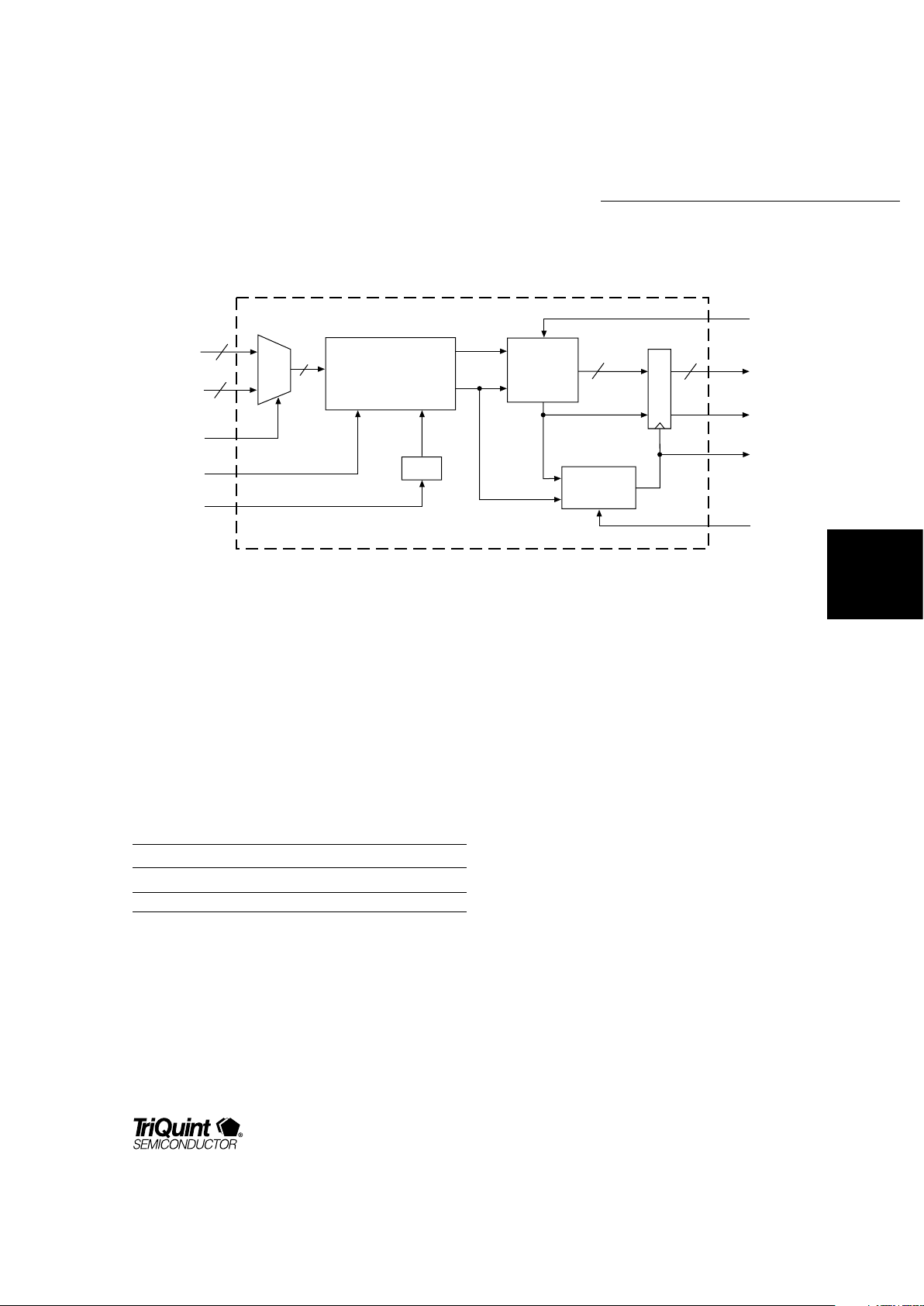
Functional Description – TQ9502 Receiver
The TQ9502 consists of a clock and data recovery
circuit, a multiplexer, and a serial-to-parallel converter
block, as shown in Figure 3. The multiplexer selects
between the RX and RY inputs or the RLX and RLY
inputs. Outputs RTX, RTY, RLTX and RLTY, not shown
on Figure 3, are provided for Fly-By
™
termination,
which allows termination resistors to be placed away
from the chip. The multiplexer output is selected by the
LOOPEN pin as shown in Table 1. The selected data
goes to the CDR (Clock/Data Recovery) block.
The clock and data recovery block has two modes:
clock recovery and frequency acquisition. In the clock
input, it automatically switches to the frequency
acquisition mode which causes the CDR to lock onto
the REFCLK signal. This prevents the PLL from drifting
away from the serial data rate and ensures that the
CDR will properly lock onto the input serial data when it
is reapplied.
The receiver synchronizes 1 ms after applying power,
REFCLK and data. The receiver synchronizes 200 µs
after applying valid data if power and REFCLK has
already been applied. The output of this block is latched
into the output register. When SYNCEN is high
(SYNCronization ENable), the serial-to-parallel
converter monitors the serial data for the K28.5
character. When it sees a K28.5, it realigns the 10-bit
register to the K28.5 character and drives SYNC high.
The clock generate block also detects SYNC going high,
and delays the phase of the output RXCLK to coincide
with the new alignment. Some bits may be lost during
the realignment. When SYNCEN is low, SYNC is driven
low and the serial-to-parallel converter ignores the
K28.5 character.
The output register takes in the 10-bit-wide output
from the Serial-to-Parallel Converter and drives the
RXD0..9 outputs. RXD0..9 are strobed on the rising
edge of RXCLK. CLKPOL = 1 results in a longer setup
time and shorter hold time than CLKPOL = 0. The first
serial bit is placed in RXD9 and the tenth bit is placed
in RXD0.
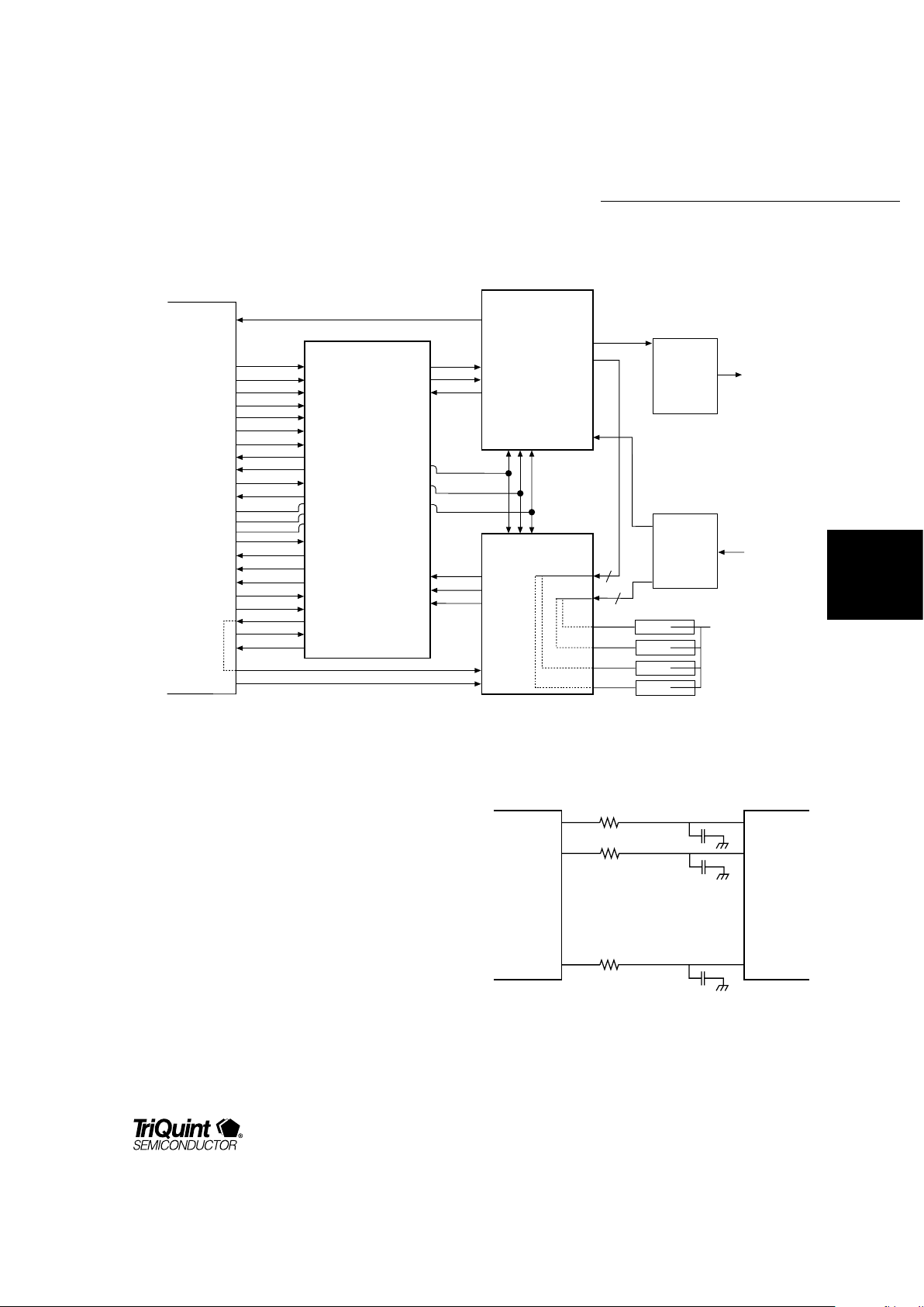
Fibre Channel Interface
Figure 3 illustrates a typical Fibre Channel physical
layer block diagram using the TQ9501, TQ9502 and
TQ9303 chip set. The interface between the host and
ENDEC operates at 26.5625 MHz with a data width of
32-bits for the transmit path and a separate 32-bits for
the receive path. The ENDEC performs the 8b/10b
encoding and decoding; ordered set encoding and
decoding; parity checking and generation; 32-bit CRC
checking and generation; and word synchronization.
The interface between the TQ9303 and the TQ9501/
TQ9502 operates at 531.25 or 106.250 MHz with an
encoded data width of 10-bits. The serial interface
operates from 531.125 Mbaud or 1.0625 Gbaud
respectively, which is connected to an optical, coaxial
or twisted pair interface.
For additional information on the ENDEC, please refer
to the TQ9303 data sheet.
Page 5
TQ9501/TQ9502
5
DATACOM
PRODUCTS
For additional information and latest specifications, see our website: www.triquint.com
Host
TQ9303 ENDEC
TQ9501 TX
TQ9502 RX
Out
In
Termination
Network
RTX
RTY
RLTX
RLTY
2
2
Optical,
Coaxial, or
Twisted Pair
Interface
Optical,
Coaxial, or
Twisted Pair
Interface
RLX, RLY
RX, RY
RXD0..9
RXCLK
SYNC
SYNCEN
CLKPOL
LOOPEN
RATESEL
SIGDET
TXD0..9
TXCLK
BYTECLK
TX, TY
TLX, TLY
SIG, SIGN
CTXD0..31
CTXC0,1
CTXP0..3
CTXRAWA,B
CTXRAW
CTXPENN
CTXPMODE
CTXPERR
CTXCERR
CTXCLK
CTXWREF
RESETN
CRXD0..31
CRXP0..3
CRXS0..5
RAWRX
RXPMODE
WRDSYNCN
RXCKPH0,1
BRXSYNC
BRXCLK
BRXD0..9
LOOPEN
REFCLK
RATESEL
BTXCKIN
BTXCKOUT
BTXD0..9
CRXCLK
REFCLK
Figure 3. System Block Diagram – Fibre Channel
Note that the fast edge rates of the TQ9303 TX bus
outputs can affect the stability of the TQ9501 PLL.
These edge rates can be effectively “slowed” by adding
some series resistance of from 90 to 250 ohms to the
TX data bus lines (TXD0..9) as shown in Figure 4.
Resistance should also be added to TXCLK to maintain
the correct timing relationship with the data lines. The
resistors should be placed near the TQ9303.
In cases where the line capacitance of the bus traces is
less than 3 pF, it may also be necessary to add from
1– 2 pf of capacitance to each trace near the TQ9501.
The purpose is to slow the edge rates enough to
prevent potential undershoot from disturbing the power
supplies in the PLL circuitry of the TQ9501.
Figure 4. Adding resistance and capacitance to
the TX data bus.
. . .
TQ9303
TQ9301
Page 6

TQ9501/TQ9502
6
For additional information and latest specifications, see our website: www.triquint.com
Figure 5. Fly-By ™ Termination Schematic
TQ9502 RX
RLTY
Z
0
= 50 Ω
Z
0
= 50 Ω
Z
0
= 50 Ω
Z
0
= 50 Ω
82 Ω
82 Ω
82 Ω
82 Ω
130 Ω
130 Ω
130 Ω
130 Ω
5V
5V
5V
5V
RLY
RLX
RLTX
RTY
RY
RX
RTX
Figure 6. Transmitter Synchronization Ciruit Block Diagram
TQ9303 ENDEC
TQ9501 TX
TXD0..9
TXCLK
BYTECLK
BTXCKIN
BTXCKOUT
BTXD0..9
Symbol Type Description
TX, TY O Differential Transmitter Outputs connect to an optical transmitter, a coaxial interface or shielded twisted pair
interface. LOOPEN low selects TY and TX outputs. LOOPEN high drives TX low and TY high.
TLX, TLY O Loopback Differential Transmitter Outputs connect to the Receiver RLX and RLY inputs. LOOPEN high selects
TLY and TLX outputs. LOOPEN low drives TLX low and TLY high.
LOOPEN I Loopback Enable high selects the TLX and TLY as outputs. LOOPEN low selects the TX and TY as outputs.
REFCLK I The PLL multiplies the Reference Clock and generates the high speed clock for transmitting serial data.
REFCLK shall be equal to 1/40 of the baud rate. REFCLK shall have a frequency tolerance of 100 ppm to
guarantee clock and data recovery on the receiver. The REFCLK operating range is 25 MHz to 31.25 MHz.
BYTECLK O The ENDEC uses Byte Clock to synchronize to the Transmitter. The ENDEC generates TXCLK from BYTECLK
simplifying the synchronization between the Transmitter and ENDEC, as shown on Figure 7.
TXD0..9 I The Transmitter latches the 10 Encoded Data Bits at the rising edge of TXCLK. The Transmitter serially
sends TXD9 first and TXD0 last.
TXCLK I The Transmitter Data Clock strobes TXD0..9 into the Transmitter. The ENDEC generates TXCLK from BYTECLK
simplifying the synchronization between the Transmitter and ENDEC.
SIG, SIGN I The Differential Signal Present are inputs to a PECL to TTL translator. The translator is typically used to
convert differential signals from a differential optical receiver output to TTL. The TTL equivalent of SIG and
SIGN is SIGDET.
SIGDET O Signal Detect is the output of the PECL to TTL translator. The translator is typically used to convert differential
signals from a differential optical receiver output to TTL. SIGDET is useful when implementing an OFC - Open
Fibre Control protocol where the link activity or optical receiver outputs are monitored continuously.
RATESEL I Rate Select is used to select between 531 Mbaud (RATESEL=VDD) and 1063 Mbaud (RATESEL=GND)
operation.
Table 2. Transmitter Pin Descriptions
Page 7

TQ9501/TQ9502
7
DATACOM
PRODUCTS
For additional information and latest specifications, see our website: www.triquint.com
Symbol Type Description
RX, RY I The Receiver Differential Inputs connects to an optical, coaxial or shielded twisted pair interface.
LOOPEN low selects the RX and RY inputs. LOOPEN high selects the RLX and RLY inputs.
RTX, RTY I The Receiver Differential Termination are used in Fly-By™
termination. RX is internally connected to
RTX and RY is internally connected to RTY. A termination circuit connects to RTX and RTY instead of
RX and RY. With Fly-By™ termination, the termination circuit can be located away from the Receiver
instead of requiring termination directly at RX and RY. Both RTX and RTY must be terminated with a
50Ω chip resistor in series with 3V reference or Thevenin equivalent as shown in Figure 6.
RLX, RLY I The Looped Receiver Differential Inputs connect to the Transmitters TLX and TLY outputs providing
a loop back path. LOOPEN high selects the RLX and RLY inputs. LOOPEN low selects the RX and RY
inputs.
RLTX, RLTY I The Receiver Differential Termination are used in Fly-By™
termination. RLX is internally connected
to RLTX and RLY is internally connected to RLTY. A termination circuit connects to RLTX and RLTY
instead of RLX and RLY. With Fly-BY™ termination, the termination circuit can be located away from
the Receiver instead of requiring termination directly at the RLX and RLY. Both RLTX and RLTY must
be terminated with a 50Ω chip resistor in series with 3V reference or Thevenin equivalent as shown
on Figure 6.
LOOPEN I Loopback Enable high selects the RLX and RLY inputs. LOOPEN low selects the RX and RY inputs.
REFCLK I The Reference Clock provides the clock needed by the clock recovery circuit. The REFCLK frequency
shall bE chosen to equal 1/40 of the baud rate. REFCLK shall have a frequency tolerance of 100 ppm
to guarantee clock and data recovery on the receiver. The receiver automatically locks onto the
REFCLK during power-up and/or when no input signals are applied. This prevents the PLL from
drifting away from the input data rate. The PLL automatically locks onto the input data stream when it
is applied. The frequency range of REFCLK is 25 MHz to 31.25 MHz.
SYNCEN I When Sync Enable is high, the receiver searches for a K28.5 character from the input data stream and
byte aligns the parallel register to this character as defined in the Fibre Channel standard. SYNCEN
low disables byte alignment to a K28.5 character and drives SYNC low. The K28.5 character has a
pattern of RXD9..0 = 001111 1010 or 110000 0101. Whenever the receiver detects the K28.5 pattern
it byte aligns to this character and drives SYNC high for that byte cycle. SYNC is high only in byte
cycle where a K28.5 character is present.
RXDO..9 O These are 10 Encoded Data Bits where the first bit received from the serial data stream is RXD9 and
the last bit received is RXD0. The receiver generates RXCLK to strobe RXD0..9.
SYNC O If SYNCEN is high, Synchronization to K28.5 goes high for the byte clock cycle in which a K28.5
character is present on the RXD0..9 output. If SYNCEN is low then SYNC is always low.
RXCLK O Receiver Data Clock is the strobe for RXD0..9 and SYNC. The phase of RXCLK with respect to
RXD0..9 and SYNC changes depending on CLKPOL. CLKPOL high provides a longer setup time and a
shorter hold time while CLKPOL low provides a shorter setup time and a longer hold time. The
frequency range of RXCLK is 50 MHz to 62.5 MHz in FC531 mode and 100 MHz to 125 MHz in FC1063
mode.
CLKPOL O Clock Phase or Polarity controls the phase of RXCLK with respect to RXD0..9 and SYNC. CLKPOL
high provides a longer setup time and a shorter hold time while CLKPOL low provides a shorter setup
time and a longer hold time.
RATESEL I Rate Select is used to select between 531 Mbaud (RATESEL=VDD) and 1063 Mbaud
(RATESEL=GND) operation.
Table 3. Receiver Pin Descriptions
Page 8

TQ9501/TQ9502
8
For additional information and latest specifications, see our website: www.triquint.com
Multiple ground and power pins on the TQ9501/02
reduce ground bounce. Good layout techniques,
however, are necessary to guarantee proper operation
and to meet the specifications across the full operating
range. TriQuint recommends bypassing each of the V
DD
supply pins to the nearest ground pin, as close to the
chip as possible.
Figure 7 shows the recommended power layout for the
TQ9501/02. The bypass capacitors should be located
on the same side of the board as the TQ9501/02. The
V
DD
traces connect to an inner-layer VDD plane. All of
the ground pins (GND) are connected to a small ground
plane on the surface beneath the chip. Multiple
through-holes connect this small surface plane to an
inner-layer ground plane. The capacitors are 0.1 µF.
TriQuint's test board uses X7R temperature-stable
capacitors in 1206 SMD cases.
Figure 7. Example Top Layer Layout of Power Pins
(Not to scale)
V
DD
V
DD
V
DD
V
DD
V
DD
V
DD
V
DD
C
C
C
C
C
C
Rx Only
Pin 1
Pin 23
Ground
Plane
Parameter Range
Storage temperature –65 °C to +150 °C
Case temperature –55 °C to +125 °C
Supply voltage to ground –0.5 V to +7.0 V
DC input voltage –0.5 V to (VDD +0.5 V)
DC input current 30 mA to +5 mA
Package Thermal ResistanceθjA = 40 °C/W; θcA = 8 °C/W
Die Junction Temperature
Tj = 150 °C
Note: Stresses above those listed in Absolute Maximum Rating
may cause permanent damage to the device. This is a
stress-only rating and operation of the device at these or any
other conditions above those indicated in the operational
section of this specification is not implied.
Layout Guidelines
Note: Series resistors and small capacitors may be needed for the
TX data bus and clock lines. See the previous “Fibre Channel
Interface” section in this datasheet for details.
Symbol Description Test Conditions Min. Typ. Max. Unit
C
IN
Input capacitance VIN = 2.0 V at f = 1 MHz 6 pF
C
OUT
Output capacitance V
OUT
= 2.0 V at f = 1 MHz 9 pF
Parameter Range
Supply voltage
5 V ± 5
Ambient temperature
0 to 70 °C
Note: Proper functionality is guaranteed under these
operating conditions.
Table 4. Absolute Maximum Ratings
Table 5. Operating Conditions
Table 6. Test Loads
Page 9

TQ9501/TQ9502
9
DATACOM
PRODUCTS
For additional information and latest specifications, see our website: www.triquint.com
Notes: 1. Typical limits are: V
DD
= 5.0 V and TA = 25 °C.
2. The TTL inputs could be HIGH or LOW.
3. The I
OL
and I
OH
specifications are valid only for the BYTECLK.
4. These are absolute values with respect to device ground.
5. No more than one output should be tested at a time. Duration of the short circuit should not exceed one second.
Table 7. DC Characteristics—TQ9501 Transmitter TTL Signals
(TXDO..9, TXCLK, BYTECLK, LOOPEN, SIGDET, REFCLK, RATESEL)
(Over operating range unless otherwise specified)
Limits
1
Symbol Description Test Conditions Min. Typ. Max. Unit
V
OH
Output HIGH voltage VDD = Min IOH = –1.6 mA 2.4 3.2 V
V
IN
2
= VIH or V
IL
IOH = –3.2 mA
3
V
OL
Output LOW voltage VDD = Min I
OL
= 4 mA 0.2 0.5 V
V
IN2
= VIH or V
IL
IOL = 8 mA
3
I
SC
4
Output short-circuit current VDD = Max V
OUT
= 0.5 V –15 –120 mA
I
IL
Input LOW current VDD = Max VIN = 0.4 V – 400 µ A
I
IH
Input HIGH current VDD = Max VIN = 2.7 V 25 µA
I
I
Input HIGH current VDD = Max VIN = 5.5 V 1 mA
V
IH
5
Input HIGH level Guaranteed input logical HIGH 2.0 V
voltage for all inputs, VDD = Max
V
IL
5
Input LOW level Guaranteed input logical LOW 0.8 V
voltage for all inputs
V
I
Input clamp voltage VDD = Min IIN = –18 mA –1.2 V
I
DD
Power supply current VDD = Max, static 175 220 mA
Table 8. DC Characteristics—TQ9501 Transmitter PECL Signals (TX, TY, TLX, TLY, SIG, SIGN)
Limits
1
Symbol Description Test Conditions Min. Typ. Max. Unit
V
OH
Output HIGH voltage VDD = Min PECL load V
DD
– 1.200 V
DD
– 0.50 V
V
OL
Output LOW voltage VDD = Min PECL load V
DD
– 2.00 V
DD
– 1.60 V
V
CMO
Output common mode voltage VDD – 1.60 VDD –1.10 V
DV
OUT
Output differential voltage 0.60 1.2 V
I
IL
Input LOW current VDD = Max VIN =2.4 V 200 µA
I
IH
Input HIGH current VDD = Max VIN = VDD – 0.5 V 250 µA
V
IHS
Highest input HIGH voltage VDD = Min VDD – 0.5 V
V
ILS
Lowest input LOW voltage VDD = Max 2.4 V
V
DIF
Differential input voltage VDD = Min 0.4 1.2 V
V
ICM
Input common mode voltage VDD = Min 2.8 VDD – 0.7 V
Page 10

TQ9501/TQ9502
10
For additional information and latest specifications, see our website: www.triquint.com
Notes: 1. Typical limits are: VDD = 5.0 V and TA = 25 °C.
2. The TTL inputs could be HIGH or LOW.
3. The I
OL
and I
OH
specifications are valid only for the RXCLK.
4. These are absolute values with respect to device ground.
5. No more than one output should be tested at a time. Duration of the short circuit should not exceed one second.
Table 9. DC Characteristics—TQ9502 Receiver TTL Signals
(RXD0..9, RXCLK, SYNCEN, REFCLK, LOOPEN, SYNC, CLKPOL, RATESEL)
(Over operating range unless otherwise specified)
Limits
1
Symbol Description Test Conditions Min. Typ. Max. Unit
V
OH
Output HIGH voltage VDD = Min IOH␣ = –1.6 mA 2.4 3.2 V
V
IN
2
= VIH or VIL ␣␣␣␣ = –3.2 mA
3
V
OL
Output LOW voltage VDD = Min IOL = 4 mA 0.2 0.5 V
V
IN
2
= VIH or V
IL
␣␣␣␣␣␣= 8 mA
3
I
SC
5
Output short–circuit current VDD = Max V
OUT
= 0.5 V –15 –120 mA
I
IL
Input LOW current VDD = Max VIN = 0.40 V –400 µA
I
IH
Input HIGH current VDD = Max VIN = 2.7 V 25 µA
I
I
Input HIGH current VDD = Max VIN = 5.5 V 1 mA
V
IH
4
Input HIGH level Guaranteed input logical HIGH 2.0 V
voltage for all inputs
V
IL
4
Input LOW level Guaranteed input logical LOW 0.8 V
voltage for all inputs
V
I
Input clamp voltage VDD = Min IIN = –18 mA –1.2 V
I
DD
Power supply current VDD = Max, static 280 350 mA
Table 10. DC Characteristics—TQ9502 Receiver PECL Signals (RX, RY, RTX, RTY, RLX, RLY, RLTX, RLTY)
Limits
1
Symbol Description Test Conditions Min. Typ. Max. Unit
I
IL
Input LOW current VDD = Max VIN = 2.4 V 0.5 200 µA
I
IH
Input HIGH current VDD = Max VIN = VDD –0.5 V 250 µA
V
IHS
Highest input HIGH voltage VDD = Max V
DD
– 0.50 V
V
ILS
Lowest input LOW voltage VDD = Min 2.4 V
V
DIF
Differential input voltage VDD = Min 0.4 1.2 V
V
ICM
Input common mode voltage VDD = Min 2.8 V
DD
– 0.7 V
Page 11

TQ9501/TQ9502
11
DATACOM
PRODUCTS
For additional information and latest specifications, see our website: www.triquint.com
Notes: 1. REFCLK Tolerance = (20/baud rate)
±
0.01%, for baud rate of 500Mbaud to 625Mbaud and
(40/baud rate)
±
0.01%, for baud rate of 1 Gbaud to 1.25 Gbaud.
2. baud time = 1/baud rate
3. The jitter numbers are for a BER of 10
–12
.
Figure 8. Bus Timing – TQ9501 Transmitter
TXD0..9
TXCLK
BYTECLK
T4
T5
T6
T7
T8
T1 T2
T3
REFCLK
TX, TLX
T10
T9
T11
80%
50%
20%
50%
TY, TLY
T12
T12
T12
T12
Figure 9.Serial Output Timing – TQ9501
Parameter Description Min. Typ. Max. Units
T
1
REFCLK pulse width HIGH 10.0 ns
T
2
REFCLK pulse width LOW 10.0 ns
T
3
1
REFCLK period (T) 32.0 40.0 ns
T
4
TXD 9..0 setup time 2.0 ns
T
5
TXD 9..0 hold time 2.0 ns
T
6
BYTECLK, TXCLK pulse width HIGH 6.0/3.0 ns
T
7
BYTECLK, TXCLK pulse width LOW 6.0/3.0 ns
T
8
BYTECLK, TXCLK period (T) 16.0/8.0 20.0/10.0 ns
T
9
TX, TY, TLX, TLY rise time 100 400/300 ps
T
10
TX, TY, TLX, TLY fall time 100 400/300 ps
T
11
TX ~ TY or TLX ~ TLY skew 100/60 ps
T
12
3
TX , TY or TLX , TLY output jitter – deterministic jitter (DJ) 100/75 ps
– random jitter (RJ) 200/150 ps
Parameters with dual values refer to 531Mbaud/1063Mbaud operation respectively.
Table 12. AC Specifications—TQ9501 Transmitter
Page 12

TQ9501/TQ9502
12
For additional information and latest specifications, see our website: www.triquint.com
Notes: 1. REFCLK Tolerance = (20/baud rate)
±
0.01%, for baud rate of 500Mbaud to 625Mbaud and (40/baud rate) ± 0.01%,
for baud rate of 1 Gbaud to 1.25 Gbaud.
2. baud time = 1/baud Rate
3. The jitter numbers are for a BER of 10
–12
.
Figure 10. Bus Timing – TQ9502 Receiver
RXD0..9
RXCLK
T24
T25
T27
T28
T26
REFCLK
T21
T22
T23
SYNC
Description Min. Typ. Max. Units
Power Up or application of REFCLK to receiver synchronization 1 ms
Application of valid data to receiver synchronization 200 µs
Receiver resynchronization after phase shift on data 2500 bit time
Parameter Description Min. Typ. Max. Units
T
21
REFCLK pulse width LOW 10.0 ns
T
22
REFCLK pulse width HIGH 10.0 ns
T
23
1
REFCLK period 32.0 40.0 ns
T
24
Setup Time RXD 0..9 & SYNC CLKPOL=0 4.0/2.0 ns
CLKPOL=1 12.0/6.0 ns
T
25
Hold Time RXD 0..9 & SYNC CLKPOL=0 8.0/4.0 ns
CLKPOL=1 0 ns
T
26
1
RXCLK period 16.0/8.0 20.0/10.0 ns
T
27
1
RXCLK pulse width HIGH 6.0/4.0 ns
T
28
1
RXCLK pulse width LOW 6.0/4.0 ns
T
29
RX, RY, RLX, RLY rise time 0.4 baud time ns
T
30
RX, RY, RLX, RLY fall time 0.4 baud time ns
T
31
RX ~ RY, RLX ~ RLY skew 0.3 baud time ns
T
32
RX, RY, RLX, RLY peak-to-peak input jitter 0.7 baud time ns
Table 12. AC Specifications—TQ9502 Receiver
Parameters with dual values refer to 531Mbaud/1063Mbaud operation respectively.
Table 13. Synchronization Times
Page 13

TQ9501/TQ9502
13
DATACOM
PRODUCTS
For additional information and latest specifications, see our website: www.triquint.com
Figure 11. Serial Input Timing – TQ9502
RX, RTX, RLX, RLTX
T29
T31
80%
50%
20%
50%
RY, RTY, RLY, RLTY
T32
T32
T30
Figure 12a. TTL Test Load,RXCLK
Figure 12b. TTL Test Load, All Other TLL Outputs
Figure 12c. PECL Test Load
680 Ω
1000 Ω
V
DD
1370 Ω
2000 Ω
V
DD
130 Ω
82 Ω
V
DD
Page 14
TQ9501/TQ9502
14
For additional information and latest specifications, see our website: www.triquint.com
Figure 13. Pinout for Transmitter
Symbol Pin # I/O # Pins Logic Type Active Description
TX, TY 20, 21 Output 2 PECL NRZ Differential serial data output
TLX, TLY 25, 26 Output 2 PECL NRZ Loopback differential serial data output
SIG, SIGN 14, 16 Input 2 PECL HIGH Differential optical signal present
TXCLK 34 Input 1 TTL HIGH Transmit clock
TXD 0..9 10, 9, 8, 5, 4, Input 10 TTL HIGH Transmit data input
2, 1, 44, 42, 41
LOOPEN 30 Input 1 TTL HIGH Enable loopback
SIGDET 38 Output 1 TTL HIGH Signal detect
REFCLK 32 Input 1 TTL HIGH Oscillator clock (25 to 31.25 MHz)
BYTECLK 37 Output 1 TTL HIGH Byte clock
VDD 6, 17, 29, 31, 35, 39 — 6 — — +5 Volt Supply
GND 7,18, 23, — 6 — — Ground
28, 33, 40
NC 3,11, 12, 13, 15, — 10 — — No Connect
19, 22, 24, 27, 43
RATESEL 36 Input 1 — — VDD (1) for 531Mbaud operation Ground
(0) for 1063Mbaud operation
Table 14. Pin Definitions – TQ9501 Transmitter
Tx
TQ9501
39
38
37
36
35
34
33
32
31
30
29
7
8
9
10
11
12
13
14
15
16
17
6 5 4 3 2 1 44 43 42 41 40
18 19 20 21 22 23 24 25 26 27 28
VDD
TXD3
TXD4NCTXD5
TXD6
TXD7NCTXD8
TXD9
GND
VDD
SIGDET
BYTECLK
RATESEL
VDD
TXCLK
GND
REFCLK
VDD
LOOPEN
VDD
GND
NC
TX
TY
NC
GND
NC
TLX
TLY
NC
GND
GND
TXD2
TXD1
TXD0
NC
NC
NC
SIG
NC
SIGN
VDD
Page 15

TQ9501/TQ9502
15
DATACOM
PRODUCTS
For additional information and latest specifications, see our website: www.triquint.com
Figure 14. Pinout for Receiver
Symbol Pin # I/O # Pins Logic Type Active Description
RX, RY 26, 25 I 2 PECL NRZ Differential serial data input
RLX, RLY 21, 20 I 2 PECL NRZ Differential serial data input, loopback
RTX, RTY 27, 24 I 2 PECL NRZ For fly-by termination
RLTX, RLTY 22, 19 I 2 PECL NRZ For fly-by termination
RXD 0..9 8, 5, 4, 2, 1, O 10 TTL HIGH Receive output data
44, 42, 41, 38, 37
RXCLK 9 O 1 TTL HIGH Receive clock
REFCLK 14 I 1 TTL HIGH Oscillator clock (25 MHz to 31.25 MHz)
SYNC 36 O 1 TTL HIGH Receive byte sync
SYNCEN 12 I 1 TTL HIGH Sync Enable or Align to K28.5
LOOPEN 16 I 1 TTL HIGH Enable loopback
CLKPOL 34 I 1 TTL LOW RXCLK Clock Phase
VDD 6, 13, 17, 29, — 8 — — +5 V supply
31, 35, 39, 43
GND 3, 7, 11, 15, 18, — 9 — — Ground
23, 28, 33, 40
NC 30, 32 — 2 — — No connect
RATESEL 10 I 1 — — VDD(1) for 531Mbaud operation
Ground(0) for 1063 Mbaud operation
Table 15. Pin Definitions - TQ9502 Receiver
Rx
TQ9502
VDD
RXD1
RXD2
GND
RXD3
RXD4
RXD5
VDD
RXD6
RXD7
GND
VDD
RXD8
RXD9
SYNC
VDD
CLKPOL
GND
NC
VDD
NC
VDD
GND
RLTY
RLY
RLX
RLTX
GND
RTY
RY
RX
RTX
GND
GND
RXDO
RXCLK
RATESEL
GND
SYNCEN
VDD
REFCLK
GND
LOOPEN
VDD
39
38
37
36
35
34
33
32
31
30
29
7
8
9
10
11
12
13
14
15
16
17
6 5 4 3 2 1 44 43 42 41 40
18 19 20 21 22 23 24 25 26 27 28
Page 16

TQ9501/TQ9502
16
For additional information and latest specifications, see our website: www.triquint.com
Ordering Information
TQ9501-MC
FC531/1063 Transmitter
TQ9502-MC
FC531/1063 Receiver
Additional Information
For latest specifications, additional product information,
worldwide sales and distribution locations, and information about TriQuint:
Web: www.triquint.com Tel: (503) 615-9000
Email: sales@tqs.com Fax: (503) 615-8900
For technical questions and additional information on specific applications:
Email: applications@tqs.com
The information provided herein is believed to be reliable; TriQuint assumes no liability for inaccuracies or
omissions. TriQuint assumes no responsibility for the use of this information, and all such information
shall be entirely at the user's own risk. Prices and specifications are subject to change without notice.
No patent rights or licenses to any of the circuits described herein are implied or granted to any third party.
TriQuint does not authorize or warrant any TriQuint product for use in life-support devices and/or systems.
Copyright © 1997 TriQuint Semiconductor, Inc. All rights reserved.
Revision 1.1.A November 1997
Figure 15. 44-Pin MQuad J-leaded Package
PIN 1
.050
BSC
.645
.690 ± .005
.645
.690
± .005
.045
X 45°
.132
.050 TYP
.610
± .015
.018 ± .004
.104 ± .01
.172 ± .0125
12
23
34
.030 ± .01
.015
X 45°
0.125
VENT PLUG
.028
 Loading...