

Page 1
T R I Q U I N T S E M I C O N D U C T O R , I N C .
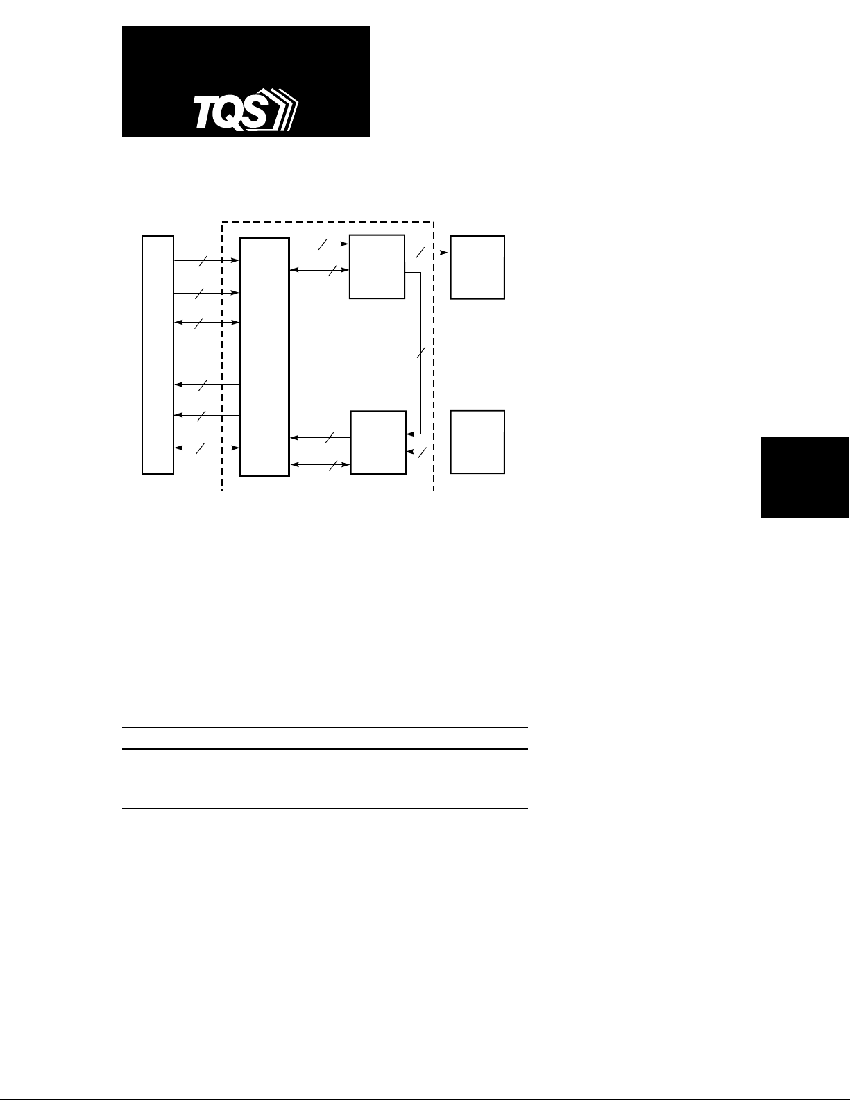
Figure 1. TQ9303 Block Diagram
HOST
Data
Parity
Control
11
Data
Parity
Control
12
Data
32
4
TQ9303
ENDEC
32
4
Control
Data
Control
TQ9501
10
10
or
GA9101
2
Tx
TQ9502
or
GA9102
Rx
2
Optical Tx
2
2
2
or
Copper
Interface
Optical Rx
or
Copper
Interface
The TQ9303 ENDEC (ENcoder/DECoder) implements 8b/10b encoding
and decoding, ordered set encoding and decoding, and parity checking
and generation as defined in the Fibre Channel Physical Signaling
Interface Standard (FC-PH). The ENDEC fully implements the FC-1 layer
of the Fibre Channel Standard. Implemented in a 0.8-micron CMOS
process, the ENDEC also performs 32-bit CRC checking and generation
as defined in the FC-2 layer of the Fibre Channel specification.
TQ9303
Fibre Channel
Encoder/Decoder
Features
• Compliant with ANSI X3T11
Fibre Channel Standard
• Full implementation of
Fibre Channel’s FC-1 layer
• Interfaces directly with
TriQuint’s GA9101/GA9102
and TQ9501/TQ9502 FC-0
Fibre Channel chipsets
• Suitable for proprietary serial
links (virtual ribbon cable)
• Implements 8b/10b encoding
and decoding
• Implements ordered set
encoding and decoding
DATACOM
PRODUCTS
The TQ9303 ENDEC interfaces directly to TriQuint’s FC-0 layer Fibre Channel
Transmitter (Tx) and Receiver (Rx) chipsets at the speeds shown below:
FC Rate Transmitter Receiver Data Rate (Mbaud)
FC-266 GA9101 GA9102 194–266
FC-531 TQ9501 TQ9502 500–625
FC-1063 TQ9501 TQ9502 1000–1250
Triquint’s Transmitter and Receiver devices are designed with TriQuint’s
proprietary 0.7-micron GaAs process. The Tx and Rx interface directly to
copper-based electrical media or to a fiber-optic module. The Transmitter
performs parallel-to-serial conversion on the encoded data and generates
the internal high-speed clock for the serial output data stream. The Receiver
recovers the clock and data from the input serial stream, performs serialto-parallel conversion, and detects and aligns on the K28.5 character.
For additional information and latest specifications, see our website: www.triquint.com
• Checks and generates 32-bit
CRC and parity
•
10-bit TTL-compatible interface
to Transmitter and Receiver
• 32-bit interface to the host
• Fully synchronous operation
• 160-pin PQFP
1
Page 2
TQ9303
Fibre Channel provides a transport vehicle for Intelligent
Peripheral Interface (IPI) and Small Computer System
Interface (SCSI) upper layer command sets, HighPerformance Parallel Interface (HIPPI) data link layer,
and other user-defined command sets. Fibre Channel
replaces the SCSI, IPI, and HIPPI physical interfaces
with a protocol-efficient alternative that provides
performance improvements over distance and speed.
Fibre Channel is optimized for predictable transfers of
large blocks of data such as those used in file transfers
between processors (such as super computers, mainframes, and super minis), storage systems (such as disk
and tape drives), communications devices, and outputonly devices (such as laser printers and raster scan
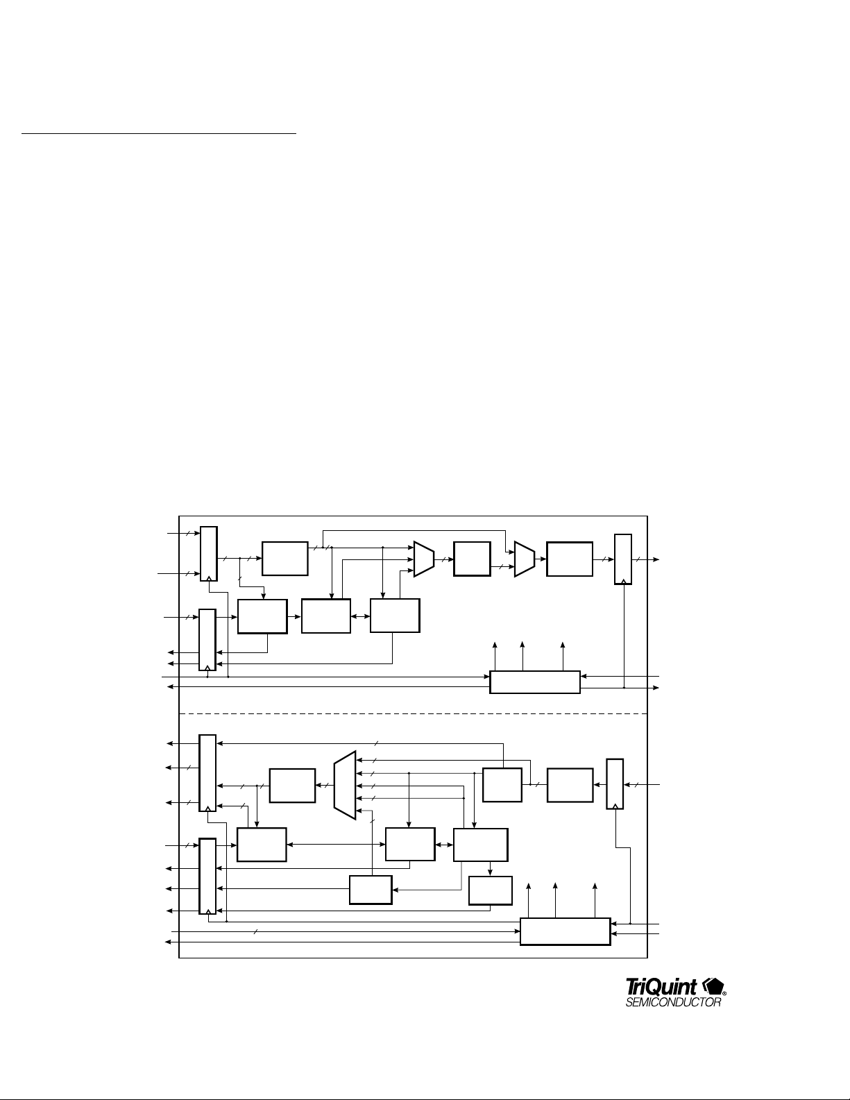
Figure 2. TQ9303 ENDEC Block Diagram
CTXD0..31
CTXC0,
CTXC1,
CTXP0..3,
CTXRAWA,
CTXRAWB
CTXRAW,
CTXPENN,
CTXPMODE
CTXPERR
CTXCERR
CTXCLK
CTXWREF
RESETN
RXERROR
CRXD0..31
CRXP0..3,
CRXS0,
CRXS2..4
RAW Rx,
RXPMODE
CRXS1
CRXS5
WRDSYNC
RXCKPH0,1
CRXCLK
32
17
Shifter
20
Ordered Set
Encoder
32-BIT CRC
Generator/
Checker
40
17
Parity
Checker/
Generator
Word-to-
Half-Word
40
Register
8
3
Register
ENCODER SECTION
DECODER SECTION
1
Mux
20
16
16
1
3
Line State
Decoder
32
Half-Word-
40
36
4
Parity
Generator
2
to-Word
Shifter
Register
8
2
Register
20
graphics terminals). The Fibre Channel protocol is
implemented in hardware, making it simple, efficient,
and robust.
The lower level physical interface is decoupled from the
higher level protocol, allowing Fibre Channel to be configured with various topologies. Point-to-point, multi-drop
bus, ring, and cross-point switch topologies are permitted in Fibre Channel, optimizing it for specific applications.
Fibre Channel supports distances up to 10␣ Km at baud
rates of 132.8125␣ Mbaud to 1.0625␣ Gbaud. Coax and
STP (Shielded Twisted Pair) are used at lower data
rates and shorter distances, while fiber-optic cables are
used for higher data rates and longer distances.
Mux
32-Bit CRC
Checker
17
8b/10b
Encoder
Ordered Set
Decoder
Word Sync
Detector
20
Word
Clk
Clock Generator
10b/8b
Decoder
Mux
Half Word
Clk
20
Word
Clk
Clock Generator
Half-Word-
to-Byte
Shifter
Byte
Clk
Byte-to-
Half-Word
Shifter
Half Word
Clk
10
Byte
Clk
10
Register
10
Register
BTXD0..9
BTXCKIN
BTXCKOUT
BRXD0..9
BRXCLK
BRXSYNC
2
For additional information and latest specifications, see our website: www.triquint.com
Page 3

Functional Description
TQ9303
The TQ9303 may be divided into two independent
functional sections: the Encoder and Decoder, as
shown in Figure 2. The Encoder section describes the
flow of data from the host to the transmitter.
Conversely, the Decoder section describes the flow of
data from the receiver to the host. Designed for fullduplex operation, the Encoder and Decoder will
transmit and receive one at a time or simultaneously.
The Encoder performs 8b/10b encoding of information
from the host to the transmitter. The Decoder performs
10b/8b decoding of information from the receiver to
the host. The host interface is denoted by a letter C (as
in
CTXP), and the transmit/receive interface is denoted
by a letter B (as in
section are denoted with the letters TX (as in C
and pins within the Decoder section are denoted with
RX (as in C
has a 32-bit transmit data bus and a 32-bit receive data
bus, each with 4-bit parity and 8-bit control. The
transmitter and receiver interfaces to the TQ9303 are
10-bit data buses. Table␣ 5 includes all the pin
descriptions. Detailed descriptions of the Encoder and
Decoder sections follow.
RXS1). At the host interface, the TQ9303
BTXD0). Pins within the Encoder
TXP),
Encoder Section
The Encoder has several functional blocks:
Parity Check, 32-Bit CRC, Ordered Set generator,
8b/10b Encoder, and Clock Generator. The Encoder
section has two modes of operation: Normal mode and
Raw mode. In the Normal mode, the Encoder section
receives a word from the host interface, checks parity,
calculates CRC, divides the word into bytes, encodes
them using 8b/10b, and generates a 10-bit output, as
illustrated in Figure 2. In the Raw mode, the Encoder
section receives a word from the host interface without
parity check, CRC check, or 8b/10b encoding.
The following is the encode sequence data flow:
1. Word input
2. Parity check
3. Word–to–half-word conversion
4. Ordered set encoding
5. 32-bit CRC check or generate
6. Muxing between ordered set, 32-bit CRC, and
unchanged input
7. 8b/10b encoding
8. Muxing between unchanged input and
encoded word
9. Half-word–to–byte conversion
10. Byte output
Parity Check Block
Parity check depends on the TXPENN (Transmit Parity
ENable Not) input. TXPENN high ignores parity, while
TXPENN low checks parity for each byte on the data
bus, CTXD0..31. There are four parity bits (CTXP0..3),
each bit corresponding to a byte of data, as follows:
CTXP0 to CTXD0..7, CTXP1 to CTXD8..15, CTXP2 to
CTXD16..23, and CTXP3 to CTXD24..31. Control bit
TXPMODE (Transmit Parity MODE) alters the normal
meaning of CTXP3. TXPMODE low is the normal mode,
where CTXP3 checks for parity for CTXD24..31. With
TXPMODE high, CTXP3 checks for parity for
CTXD24..31 and CTXC0. CTXC0 is a control input
which indicates whether CTXD0..31 is data or an
ordered set. An ordered set is a Fibre Channel word
where the most significant byte is composed of a valid
special character, K28.5, as defined in the standard.
Appendix A includes a table of valid special characters.
The parity bits follow odd parity convention, where it is
high if the number of ones is even and low if the
number of ones is odd.
DATACOM
PRODUCTS
For additional information and latest specifications, see our website: www.triquint.com
3
Page 4
TQ9303
CTXPERR (Transmit Parity ERRor) is driven high
when an error is detected in the parity check mode.
When parity checking is disabled, CTXPERR is driven
low. In Raw Mode transmit, where the data
flow
bypasses the parity check, 32-bit CRC, 8b/10b encoder,
and ordered set encoder, CTXPERR is driven low.
32-Bit CRC Block
32-bit Cyclic Redundancy Checking (CRC) generates
or checks CRC, depending on CTXC1. CTXC1 high
generates CRC, while CTXC1 low checks CRC for the
incoming frame. The CRC used in Fibre Channel is the
same as FDDI's frame check sequence, where a 32bit CRC is computed for every frame, starting after
SOF (Start Of Frame) and ending a byte before EOF
(End Of Frame). The resulting 32-bit CRC is
automatically inserted into the frame before EOF.
In the check CRC mode, CTXCERR (Transmit Crc
ERRor) is driven high when a CRC error is detected.
In the generate CRC mode, CTXCERR is driven low. In
Raw Mode transmit where the data flow bypasses the
parity check, 32-bit CRC, 8b/10b encoder, and ordered
set encoder, CTXCERR is driven low.
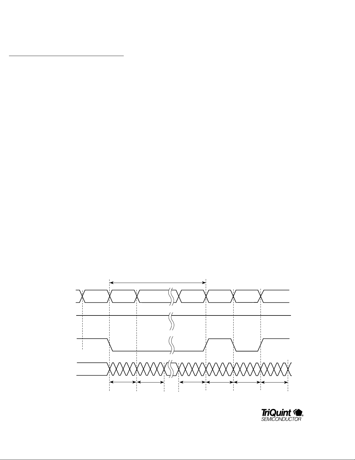
The Generate CRC mode timing diagrams are shown in
Figure 3. CTXC1 is high for the entire frame, when
generating CRC. CTXC0 is high only for the duration of
SOF, indicating that the input word (CTXD0..31) is an
ordered set. Similarly, CTXC0 is high for the duration of
EOF, which is another ordered set. The 32-bit CRC
block computes the CRC for data after SOF and before
EOF. The resulting CRC is inserted between the last
data word and EOF at the output (BTXD0..9).
The Check CRC mode timing diagrams are shown in
Figure 4. CTXC1 is low for the whole frame when
checking CRC. CTXC0 is high only for the duration of
SOF, indicating that the input word (CTXD0..31) is an
ordered set. Similarly, CTXC0 is high for the duration of
EOF, another ordered set. 32-bit CRC begins after SOF
Figure 3. Generate CRC Mode TIming
CTXD0..31
CTXC1
CTXC0
BTXD0..9
4
SOF
For additional information and latest specifications, see our website: www.triquint.com
D0
4 Bytes
SOF
CRC Computation
D1
D0
Dn
Dn-1
EOF
Dn
"d"
CRC
Idle
EOF
Page 5
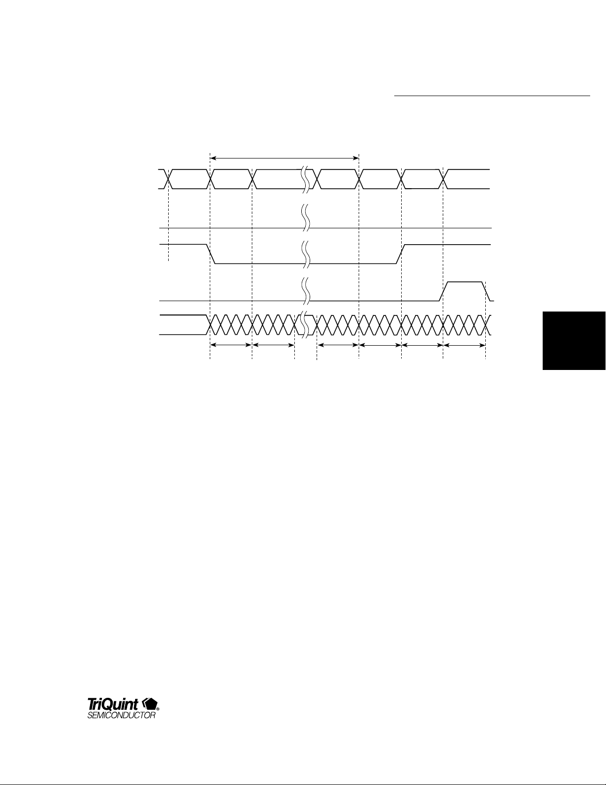
Figure 4. Check CRC Mode TIming
TQ9303
CRC Computation
CTXD0..31
CTXC1
CTXC0
CTCXERR
BTXD0..9
SOF
D0
4 Bytes
SOF
D1
D0
and ends before EOF. CTXCERR remains low if the
computed CRC matches the CRC input on CTXD0..31.
CTXCERR is driven high for one word cycle after the
end of EOF.
If CTXC1␣ is␣ high (generate CRC) then the ENDEC will
add one word (the CRC) to the user’s data frame before
encoding the EOF. In this situation, when the user
commands the ENDEC to encode an EOF, it is latched
for one CTXCLK cycle while the ENDEC inserts the
generated CRC in the data stream. Then the requested
EOF is encoded. During the encoding of the EOF (that
is, the one that was latched for encoding after the CRC
was inserted) the ENDEC ignores the CTX inputs.
Ordered Set Generator Block
An ordered set is a Fibre Channel word in which the
first byte is a K28.5 special character, followed by valid
data characters. Appendix B contains tables for the
ordered set coding scheme. When CTXC0 is high, the
ordered set generator generates an ordered set from
Dn
Dn-1
CRC
Dn
EOF
CRC
Idle
EOF
the most significant byte of the input data, CTXD24..31.
Although only the most significant byte of the input
word is required for generating an ordered set, and
lower order bits CTXD0..23 are “don’t cares” for
encoding the ordered set, parity checking is performed
on the word. Valid word parity must be maintained to
prevent parity errors.
If a parity or CRC error is detected within a frame,
some EOF ordered sets are modified, indicating an
invalid frame. Ordered sets EOF
EOF
(EOF Terminate) are modified to EOFNI (EOF
T
(EOF Normal) and
N
Normal–Invalid).
Any ordered set can be sent or received. If the ordered
set desired is not in the predefined set of Fibre Channel
ordered sets, the user can create it using the “special”
ordered set commands (see Appendix B). For instance,
to send “K28.5, D0.0, D31.7, D0.0,” the user would
send 8500FF00h on CTXD0..31 while holding CTXC0
high. When receiving this same “special” ordered set
DATACOM
PRODUCTS
For additional information and latest specifications, see our website: www.triquint.com
5
Page 6

TQ9303
(which does not correspond to any predefined Fibre
Channel ordered set) the ENDEC will send the user the
same value, 8500FF00h, while holding CRXS0 high. It
is up the the user to examine the second, third, and
fourth bytes of “special” ordered sets to identify them.
8b/10b Encoder Block
The 8b/10b Encoder encodes 8-bit-wide data to 10-bitwide data to improve its transmission characteristics.
The 8b/10b coding scheme maintains the signal DC
balance by keeping the same number of ones and zeros
for easier receiver designs, provides good transition
density for improved clock recovery, and improves
error checking. It also forces the correct running
disparity when encoding line states, idles, or receiverready ordered sets. Appendix A contains the lookup
tables for the 8b/10b coding scheme.
Clock Generator Block
The Clock Generator generates word, half-word, and
byte clocks required by other blocks in the Encoder. It
uses BTXCKIN (a byte clock) from the transmitter as a
reference clock. For example, using Fibre Channel data
rates, BTXCKIN runs at 106.25␣ MHz using FC1063,
53.125␣ MHz using FC531, and 26.5625␣ MHz using
FC266. The Clock Generator generates BTXCKOUT for
clocking BTXD0..9. It also generates CTXWREF, a word
clock used by the host to generate CTXCLK, which
clocks the host I/O registers.
25.5625␣ MHz using FC1063,
CTXCLK runs at
13.28125␣ MHz using
FC531, and 6.640625␣ MHz using FC266.
Raw Mode Transmit
In Raw Mode Transmit where TXRAW is high for the
whole frame, the input data word bypasses the parity
check, ordered set generator, CRC, and 8b/10b, and is
directly converted to bytes of data. The word-to-byte
mapping of input to output is listed in Table␣ 1. Note that
in raw mode, a “raw” word may be inserted into the
data flow at any time, although running disparity will be
forced negative and the word sync detector state
machine will reset.
Proprietary Link Mode
The PL_IDLE (Proprietary Link IDLE) input can be used
to simplify designs that do not have to conform to Fibre
Channel standards. In such designs the CTXC0 input is
driven low (that is, grounded) and the PL_IDLE pin is
used to distinguish data from nondata. The PL_IDLE
pin controls a bit logic in front of the input registers of
the CTXC0 and CTXD24..31 inputs. It was added to
make it easier for users who aren’t concerned with the
Fibre Channel protocol, but simply want to control the
transmission of data without habing to mux control
information into their data paths in order to control the
CTXD24..31 pins for ordered set control.
On the rising edge of CTXCLK on the first cycle of
PL_IDLE going high, the input registers for CTXC0 and
CTXD24..31 are “jammed” with the value that would
make the ENDEC encode an EOFa. As long as PL_IDLE
is held high, these input registers are jammed with the
value that would make the ENDEC encode an IDLE
ordered set. If CTXC1 is low (check mode) CTXERR will
properly reflect the validity of CRC contained in the
user’s data (assuming the user’s data contains CRC), or
it can be ignored if no CRC is used. If CTXC1 is high
(generate mode), the ENDEC will insert CRC before
encoding the EOFa followed by IDLEs. This creates a
situation in which the user’s data will begin as soon as
PL_IDLE is dropped (with no preceding SOF); but it
does not present a problem for the ENDEC, because the
CRC blocks in both Rx and Tx halves are initialized by
any ordered set. Thus, the IDLE ordered set that
preceeds the user’s data is sufficient to ensure proper
CRC calculation.
6
For additional information and latest specifications, see our website: www.triquint.com
Page 7

Table 1. Raw Mode I/O Mapping
TQ9303
TRANSMISSION ORDER
FIRST
BYTE
FIRST SERIAL BIT IN TX/RX
SECOND
BYTE
THIRD
BYTE
LAST SERIAL BIT IN TX/RX
FOURTH
BYTE
Bit ENCODE: Word to Bytes DECODE: Bytes to Word
39 CTXC0 BTXD0 BRXD0 CRXS0
38 CTXP3 BTXD1 BRXD1 CRXP3
37 CTXD31 BTXD2 BRXD2 CRXD31
36 CTXD30 BTXD3 BRXD3 CRXD30
35 CTXD29 BTXD4 BRXD4 CRXD29
34 CTXD28 BTXD5 BRXD5 CRXD28
33 CTXD27 BTXD6 BRXD6 CRXD27
32 CTXD26 BTXD7 BRXD7 CRXD26
31 CTXD25 BTXD8 BRXD8 CRXD25
30 CTXD24 BTXD9 BRXD9 CRXD24
29 CTXC1 BTXD0 BRXD0 CRXS2
28 CTXP2 BTXD1 BRXD1 CRXP2
27 CTXD23 BTXD2 BRXD2 CRXD23
26 CTXD22 BTXD3 BRXD3 CRXD22
25 CTXD21 BTXD4 BRXD4 CRXD21
24 CTXD20 BTXD5 BRXD5 CRXD20
23 CTXD19 BTXD6 BRXD6 CRXD19
22 CTXD18 BTXD7 BRXD7 CRXD18
21 CTXD17 BTXD8 BRXD8 CRXD17
20 CTXD16 BTXD9 BRXD9 CRXD16
19 CTXRAWA BTXD0 BRXD0 CRXS3
18 CTXP1 BTXD1 BRXD1 CRXP1
17 CTXD15 BTXD2 BRXD2 CRXD15
16 CTXD14 BTXD3 BRXD3 CRXD14
15 CTXD13 BTXD4 BRXD4 CRXD13
14 CTXD12 BTXD5 BRXD5 CRXD12
13 CTXD11 BTXD6 BRXD6 CRXD11
12 CTXD10 BTXD7 BRXD7 CRXD10
11 CTXD9 BTXD8 BRXD8 CRXD9
10 CTXD8 BTXD9 BRXD9 CRXD8
9 CTXRAWB BTXD0 BRXD0 CRXS4
8 CTXP0 BTXD1 BRXD1 CRXP0
7 CTXD7 BTXD2 BRXD2 CRXD7
6 CTXD6 BTXD3 BRXD3 CRXD6
5 CTXD5 BTXD4 BRXD4 CRXD5
4 CTXD4 BTXD5 BRXD5 CRXD4
3 CTXD3 BTXD6 BRXD6 CRXD3
2 CTXD2 BTXD7 BRXD7 CRXD2
1 CTXD1 BTXD8 BRXD8 CRXD1
0 CTXD0 BTXD9 BRXD9 CRXD0
DATACOM
PRODUCTS
For additional information and latest specifications, see our website: www.triquint.com
7
Page 8

TQ9303
Proprietary Link Mode (continued)
When PL_IDLE is driven low, data words on CTXD0..31
are encoded just as in Fibre Channel operation. When
PL_IDLE is driven high, the TQ9303 encodes one EOFa
ordered set followed by IDLE ordered sets for as long
as PL_IDLE remains high.
The EOFa ordered set is used to ensure proper running
disparity. When using the PL_IDLE signal, IDLE
ordered sets do not force proper running disparity. It is
therefore necessary to transmit at least one word with
PL_IDLE low followed by at least one word with
PL_IDLE high in order to guarantee proper running
disparity.
Without proper running disparity, the receiver portion
of the TQ9303 may flag the IDLE ordered sets as
errors and prevent the word sync state machine from
reaching the synchronized state as long as the running
disparity is incorrect.
Without proper running disparity, the receiver portion
of the TQ9303 may flag the IDLE ordered sets as errors
and prevent the word sync state machine from
reaching the synchronized state as long as the running
disparity is incorrect.
The contents and parity of CTXD0..31 and CTXP0..3 are
ignored during the word cycles when PL_IDLE is held
high. If CTXC1 is low, then CRC checking will occur,
which may cause the TXCERR signal to indicate an
error, which can be ignored in proprietary designs. If
CTXC1 is driven high, then the TQ9303 will generate a
32-bit CRC word during the first word cycle of PL_IDLE
high. During the second word cycle of PL_IDLE high,
the EOFa will be encoded followed by IDLE ordered
sets. Therefore, at least two word cycles of PL_IDLE
high between data bursts must be provided when using
CRC generation (that is, CTXC1␣ high). When using CRC
generation, the CRXS1 signal is used to indicate CRC
errors. When not using the CRC, CRXS1 should be
ignored. For non-Fibre Channel designs making use of
the PL_IDLE input, the CRXSO output can be used to
distinguish received data from idle time.
Decoder Section
The Decoder has several functional blocks:
10b/8b Decoder, Ordered Set Decoder, Word Sync
Detector, Line State Decoder, 32-bit CRC Checker,
Parity Generator, and Clock Generator.
The Decoder section has two modes of operation: the
Normal mode and Raw mode. In the Normal mode, the
Decoder section takes 10 bits of data from the Receiver
output, decodes it using 10b/8b, decodes ordered sets,
checks CRC, combines four bytes into a single word
output, and generates parity. In the Raw mode, the
Decoder section directly combines the bytes into
words, bypassing 10b/8b decoding, ordered set
decoding, CRC checking, and parity generation.
The following is the decode sequence data flow:
1. Byte Input
2. Byte–to–Half-Word Conversion
3. 10b/8b Decoding
4. Ordered Set Decoding
5. Line State Decoding
6. Word Sync Generation
7. 32-Bit CRC Checking
8. Muxing between Ordered Set, Unchanged Input,
10b/8b Decoded Input, and Status Bits
9. Half-Word–to–Word Conversion
10. Parity Generation
11. Word Output
8
For additional information and latest specifications, see our website: www.triquint.com
Page 9

TQ9303
10b/8b Decoder Block
The 10b/8b Decoder decodes the 10-bit input
(BRXD0..9) into 8 bits, as defined by the Fibre Channel
8b/10b coding scheme. The 10b/8b Decoder drives the
RXERROR (Receiver ERROR) high whenever errors are
detected. There are three types of errors: invalid
characters, invalid running disparities, and special
characters that are not positioned in the most
significant byte of a word. When the 10b/8b Decoder
receives a BRXSYNC of 1, it identifies the input data
byte as a K28.5 character and realigns the data in the
higher order byte of the half word. In Fibre Channel,
K28.5 characters appear only in the most significant
byte of a valid generated parity word. RXERROR remains
high for the word cycle in which the error occurred.
Ordered Set Decoder Block
The Ordered Set Decoder decodes the ordered sets
from the 10b/8b Decoder output. It generates the
decoded ordered set, which is then fed into the mux
along with CRXS0. CRXS0 is a status signal which is
low for a data word and high for an ordered set. The
ordered set decoding table is included in Appendix␣ B.
Word Sync Detector Block
Figure 5. Sync State Flow Diagram
RESET or RAW Mode
STATE 0
Loss of Word Sync
WSYNC = 0
Three Ordered Sets
Without Errors
STATE 1
Acquired Word Sync
WSYNC = 1
Invalid Word
STATE 2
1st Invalid Word
WSYNC = 1
Invalid Word
STATE 3
Two Consecutive
Valid Words
2nd Invalid Word
WSYNC = 1
Invalid Word
STATE 4
3rd Invalid Word
WSYNC = 1
Invalid Word
Invalid
Word
Two Consecutive
Valid Words
Two Consecutive
Valid Words
DATACOM
PRODUCTS
The Word Sync Detector contains a state machine that
monitors the number of valid ordered sets and errors
received. The Word Sync Detector drives WRDSYNCN
low to indicate that word synchronization on the link
has been established. It drives WRDSYNCN high
when word synchronization has been lost.
Figure␣ 5 illustrates how word synchronization is
established and lost. The state machine has five states:
State␣ 0␣ – Loss of Word Sync, State␣ 1␣ – Word Sync
Acquired, State␣ 2␣ – 1st Invalid Word, State␣ 3␣ – 2nd
Invalid Word, and State␣ 4␣ – 3rd Invalid Word. Upon
RESET or Raw mode at State␣ 0, the initial condition of
For additional information and latest specifications, see our website: www.triquint.com
WRDSYNCN is high. If the Word Sync Detector
receives three consecutive ordered sets without errors,
it acquires word synchronization and moves to State␣ 1,
where WRDSYNCN is driven low. If it receives an
invalid word while in State␣ 1, it moves to State␣ 2 (1st
Invalid Word). If the Word Sync Detector receives an
invalid word while in State␣ 2, it moves to State␣ 3 (2nd
Invalid Word). If, however, it receives two consecutive
valid words, it moves back to State␣ 1. This logic applies
to State␣ 3 and State␣ 4. In State␣ 4 (3rd Invalid Word) if
the Decoder receives an invalid word, it moves to
State␣ 0 (Loss of Word Sync).
9
Page 10

TQ9303
Line State Decoder Block
The state machine that indicates line state status
simply looks for three consecutive line state primitives
(that is, three of a kind in a row) to achieve a particular
Fibre Channel line state. Line states are used in link
initialization protocol, as described in the Fibre Channel
specification (FC-PH). A subset of the ordered sets, line
states are Fibre Channel primitive sequences which
provide information regarding the condition of the link.
The following are the four line states:
• Off-Line State (OLS) indicates either an internal
port failure or a transmitter power down/
diagnostics performance / initialization.
• Non-Operational State (NOS) signals a link failure.
• Link Reset (LR) recognizes the OLS and port reset
conditions.
• Link Reset Response (LRR) recognizes a link reset.
These line states are defined in Appendix␣ B. The Line
State Decoder generates CRXS2..3, the line state status
bits which advise the host as to the state of the Sync
State Machine, and CRXS4..5, the line state ID bits
which signal the occurrance of certain primitive
sequences. The status bits are shown in Tables 2 and 3.
Parity Generator Block
Four parity bits (CTXP0..3) are generated by the Parity
Generator. Each parity bit corresponds to a byte of
data, as follows: CRXP0 to CRXD0..7, CRXP1 to
CRXD8..15, CRXP2 to CRXD16..23, and CRXP3 to
CRXD24..31.
Control bit RXPMODE (Receive Parity MODE) alters the
normal meaning of CRXP3. RXPMODE low is the
normal mode, where CRXP3 generates parity for
CRXD24..31. With RXPMODE high, however, CRXP3
generates parity for CRXD24..31 and CRXS0. CRXS0 is
a control output that indicates whether CTXD0..31 is
data or an ordered set.
The parity bits follow odd parity convention, where it is
high if the number of ones is even and low if the
number of ones is odd.
In Raw mode, the Parity Generator does not generate
parity, and the output parity bits are mapped with the
input data as shown in Table␣ 1.
Clock Generator Block
32-Bit CRC Checker Block
The CRC Checker computes the 32-bit cyclic
redundancy check on the received data. The CRC Error
Status bit CRXS1 is driven high when an error is
detected. In Raw mode, CRC is not checked, and
CRXS1 is driven low.
Table 2. Line State Status Output
CRXS3 CRXS2 Line State Status
0 0 No State
0 1 Pending State
1 0 In State
1 1 Invalid Sequence
10
For additional information and latest specifications, see our website: www.triquint.com
The Clock Generator generates word, half-word, and
byte clocks required by other blocks in the Decoder.
The Clock Generator uses the recovered clock, BRXCLK
generated by the TQ9502 Receiver. For example, using
Fibre Channel data rates, BRXCLK (a byte clock) runs at
106.25␣ MHz using FC1063, 53.125␣ MHz using FC531,
and 26.5625␣ MHz using FC266.
Table 3. Line State ID Output
CRXS5 CRXS4 Line State ID
0 0 NOS – Non-Operational State
0 1 OLS – Off-Line State
1 0 LR – Link Reset
1 1 LRR – Link Reset Response
,
Page 11

TQ9303
The Clock Generator generates CRXCLK, a word clock,
which is used for clocking the host I/O registers. The
user may place the clock edge, CRXCLK, in four places
relative to the word input, thereby giving the user
control of setup and hold times. Clock edge placement
is selected via control pins RXCKPH0 and RXCKPH1
(Receiver ClocK PHase). CRXCLK runs at 26.5625␣ MHz
using FC1063 and 13.28125␣ MHz using FC531.
Figure 6. Pinout
CTXD15
CTXD14
CTXD13
CTXD12
CTXD11
CTXD10
CTXD9
VSS2
CTXD8
CTXP0
CTXD7
VDD3
CTXD6
CTXD5
CTXD4
CTXD3
CTXD2
CTXD1
143
144
145
146
147
148
149
150
151
152
153
154
155
156
157
158
159
160
CTXD0
VSS1
BTXD0
BTXD1
BTXD2
VSS1
BTXD3
BTXD4
VDD
BTXD5
BTXD6
VSS1
BTXD7
BTXD8
BTXD9
VSS1
BTXCKIN
VSS1
BTXCKOUT
VDD
BRXCLK
VSS3
BRXD0
BRXD1
BRXD2
BRXD3
VDD3
BRXD4
BRXD5
BRXD6
BRXD7
VSS3
BRXD8
BRXD9
BRXSYNC
VDD
CRXD0
CRXD1
VSS1
CRXD2
1
2
3
4
5
6
7
8
9
10
11
12
13
14
15
16
17
18
19
20
21
22
23
24
25
26
27
28
29
30
31
32
33
34
35
36
37
38
39
40
Pin 1
TQ9303
414243444546474849505152535455565758596061626364656667686970717273747576777879
The Clock Generator also receives the BRXSYNC signal,
which is used for byte alignment. The Receiver drives
BRXSYNC high when detecting a K28.5 character.
Raw Mode Receive
In Raw Mode Receive where RXRAW is high for the
whole frame, the input data word bypasses the parity
check, ordered set generator, 32-bit CRC, and 8b/10b
encoder, and is directly converted to data words. The
byte-to-word mapping of data is listed in Table␣ 1.
CTXP3
CTXD31
CTXD30
CTXD29
CTXD28
CTXD27
CTXD26
CTXD25
CTXD24
VSS2
CTXP2
CTXD23
CTXD22
VSS3
CTXD21
CTXD20
CTXD19
CTXD18
CTXD17
VDD
CTXD16
CTXP1
121
122
123
124
125
126
127
128
129
130
131
132
133
134
135
136
137
138
139
140
141
142
120
119
118
117
116
115
114
113
112
111
110
109
108
107
106
105
104
103
102
101
100
99
98
97
96
95
94
93
92
91
90
89
88
87
86
85
84
83
82
81
80
CTXC0
CTXC1
CTXRAWA
CTXRAWB
CTXCERR
CTXPERR
TXPENN
PL_IDLE
CTXCLK
TSTMODE
CTXWREF
VSS1
TXPMODE
TXRAW
RXRAW
VSS3
RXPMODE
VSS2
RXCKPH1
RXCKPH0
VDD3
RESETN
VSS1
CRXCLK
VSS1
WRDSYNCN
RXERROR
CRXS5
CRXS4
VSS1
CRXS3
CRXS2
CRXS1
VDD
CRXS0
CRXP3
CRXD31
VSS1
CRXD30
CRXD29
DATACOM
PRODUCTS
CRXD3
VDD
CRXD4
CRXD5
VSS1
CRXD6
CRXD7
CRXP0
CRXD8
VSS1
CRXD9
CRXD10
CRXD11
VDD
CRXD12
CRXD13
VSS1
CRXD14
CRXD15
VSS2
CRXP1
CRXD16
VSS1
CRXD17
CRXD18
CRXD19
VDD
CRXD20
CRXD21
VSS1
CRXD22
CRXD23
CRXP2
CRXD24
VSS1
CRXD25
For additional information and latest specifications, see our website: www.triquint.com
CRXD26
VDD
CRXD27
CRXD28
11
Page 12

Table 4. Pin Names
TQ9303
Pin Description
1 CTXD0
2 VSS
3 BTXD0
4 BTXD1
5 BTXD2
6 VSS
7 BTXD3
8 BTXD4
9 VDD
10 BTXD5
11 BTXD6
12 VSS
13 BTXD7
14 BTXD8
15 BTXD9
16 VSS
17 BTXCKIN
18 VSS
19 BTXCKOUT
20 VDD
21 BRXCLK
22 VSS
23 BRXD0
24 BRXD1
25 BRXD2
26 BRXD3
27 VDD
28 BRXD4
29 BRXD5
30 BRXD6
31 BRXD7
32 VSS
33 BRXD8
34 BRXD9
35 BRXSYNC
36 VDD
37 CRXD0
38 CRXD1
39 VSS
40 CRXD2
Pin Description
41 CRXD3
42 VDD
43 CRXD4
44 CRXD5
45 VSS
46 CRXD6
47 CRXD7
48 CRXP0
49 CRXD8
50 VSS
51 CRXD9
52 CRXD10
53 CRXD11
54 VDD
55 CRXD12
56 CRXD13
57 VSS
58 CRXD14
59 CRXD15
60 VSS
61 CRXP1
62 CRXD16
63 VSS
64 CRXD17
65 CRXD18
66 CRXD19
67 VDD
68 CRXD20
69 CRXD21
70 VSS
71 CRXD22
72 CRXD23
73 CRXP2
74 CRXD24
75 VSS
76 CRXD25
77 CRXD26
78 VDD
79 CRXD27
80 CRXD28
Pin Description
81 CRXD29
82 CRXD30
83 VSS
84 CRXD31
85 CRXP3
86 CRXS0
87 VDD
88 CRXS1
89 CRXS2
90 CRXS3
91 VSS
92 CRXS4
93 CRXS5
94 RXERROR
95 WRDSYNCN
96 VSS
97 CRXCLK
98 VSS
99 RESETN
100 VDD
101 RXCKPH0
102 RXCKPH1
103 VSS
104 RXPMODE
105 VSS
106 RXRAW
107 TXRAW
108 TXPMODE
109 VSS
110 CTXWREF
111 TSTMODE
112 CTXCLK
113 PL_IDLE
114 TXPENN
115 CTXPERR
116 CTXCERR
117 CTXRAWB
118 CTXRAWA
119 CTXC1
120 CTXC0
Pin Description
121 CTXP3
122 CTXD31
123 CTXD30
124 CTXD29
125 CTXD28
126 CTXD27
127 CTXD26
128 CTXD25
129 CTXD24
130 VSS
131 CTXP2
132 CTXD23
133 CTXD22
134 VSS
135 CTXD21
136 CTXD20
137 CTXD19
138 CTXD18
139 CTXD17
140 VDD
141 CTXD16
142 CTXP1
143 CTXD15
144 CTXD14
145 CTXD13
146 CTXD12
147 CTXD11
148 CTXD10
149 CTXD9
150 VSS
151 CTXD8
152 CTXP0
153 CTXD7
154 VDD
155 CTXD6
156 CTXD5
157 CTXD4
158 CTXD3
159 CTXD2
160 CTXD1
12
For additional information and latest specifications, see our website: www.triquint.com
Page 13

TQ9303
Table 5. Pin Descriptions
Symbol I/O # of I/O Interface Description Pin Numbers
BTXCKIN I 1 Transmitter Takes clock from Transmitter to generate BTXCKOUT. 17
BTXCKOUT O 1 Transmitter Used by Transmitter to clock in BTXD0..9. 19
BTXD0..9 O 10 Transmitter Data Output. 3–5, 7, 8, 10, 11, 13–15
CTXWREF O 1 Host Reference Word Clock which can be used in signaling the 110
host to issue a CTXCLK.
CTXCLK I 1 Host Word Clock generated from CTXCLK to clock in/out host I/O 112
registers. The following signals are latched by CTXCLK:
CTXP0..3, CTXC0,1, CTXRAW, CTXPENN, CTXPMODE,
CTXPERR, CTXCERR.
CTXC0 I 1 Host High indicates CTXD0..31 is an Ordered Set; 120
Low indicates data.
CTXC1 I 1 Host High generates CRC; low checks CRC. 119
CTXD0..31 I 32 Host Transmit data output (CTXD31 = MSB; CTXD0 = LSB). 1, 160–155, 153-151,
149–143, 141, 139–135,
133, 132, 129–122
CTXP0 I 1 Host CTXD0..7 Odd Parity input. 152
CTXP1 I 1 Host CTXD8..15 Odd Parity input. 142
CTXP2 I 1 Host CTXD16..23 Odd Parity input. 131
CTXP3 I 1 Host CTXD24..31 and optional CTXC0 Odd Parity input. 121
If TXPMODE is high, CTXP3 checks parity for
CTXD24..31 and CTXC0. If TXPMODE is low,
CTXP3 checks parity for CTXD24..31 only.
CTXRAWA I 1 Host Raw data bit 19. 118
CTXRAWB I 1 Host Raw data bit 9. 117
CTXPERR O 1 Host CTXPERR high indicates CTXD0..31 Parity Error. 115
CTXCERR O 1 Host CTXCERR high indicates CRC Error. 116
When in CRC Check mode, CTXC1 is low.
TSTMODE I 1 Host Normally GND. HIGH state used by vendor to monitor 111
delay and threshold.
TXRAW I 1 Host High selects Raw Transmit Data mode. 107
TXPENN I 1 Host Active Low Transmit Parity Enable; Tx checks Parity 114
when low.
TXPMODE I 1 Host If TXPMODE is high, CTXP3 generates parity for 108
CTXD24..31 and CTXC0. If TXPMODE is low,
CTXP3 generates parity for CTXD24..31 only.
PL_IDLE I 1 Host Proprietary link idle control 113
BRXCLK I 1 Receiver Driven by RXCLK. Clocks data from BRXD0..9. 21
BRXD0..9 I 10 Receiver Receives RXD0..9 from Receiver. 23–26, 28–31, 33, 34
BRXSYNC I 1 Receiver SYNC. 35
CRXCLK O 1 Host CRXCLK latches CRXDO..31. 97
DATACOM
PRODUCTS
(Continued on next page)
For additional information and latest specifications, see our website: www.triquint.com
13
Page 14

TQ9303
Table 5. Pin Descriptions (continued)
Symbol I/O # of I/O Interface Description Pin Numbers
CRXD0..31 O 32 Host Receive data output (CRXD31 = MSB; CRXD0 = LSB). 37,38,40,41,43,44,
CRXS0 O 1 Host High indicates CRXD0..31 is an Ordered Set; 86
CRXS1 O 1 Host CRC error flag; high indicates a CRC error. 88
CRXS2,3 O 2 Host Line state status bits. State equivalent for CRXS3 89,90
CRXS4,5 O 2 Host Line state ID bits. 92,93
CRXP0 O 1 Host CRXD0..7 Odd Parity output. 48
CRXP1 O 1 Host CRXD8..15 Odd Parity output. 61
CRXP2 O 1 Host CRXD16..23 Odd Parity output. 73
CRXP3 O 1 Host CRXD24..31 and optional CRXS01 Odd Parity output. 85
RXERROR O 1 Host Receive Error; high indicates invalid data from the Receiver. 94
RXRAW I 1 Host High selects Raw Receive Data mode. 106
WRDSYNCN O 1 Host Word Synchronization Status Flag; 95
RXPMODE I 1 Host Receiver Parity mode. If RXPMODE is high, CRXP3 104
RXCKPH0,1 I 2 Host CRXCLK Phase Select pin. 101,102
RESETN I 1 Host Active low. 99
VDD — — — +5 Volt supply. 9,20,27,36,42,54,67,
GND (V
) — — — Ground. 2,6,12,16,18,22,32,39,
SS
Low indicates data.
and CRXS2 from left to right, respectively:
␣␣␣␣00 - No State 01 - Pending
␣␣␣␣10 - State Rec. 11 - Bad Seq.
If RXPMODE is high, CRXP3 generates Parity for
CRXD24..31 and CRXS0. If RXPMODE is low,
CRXP3 generates Parity for CRXD24..31 only.
Low indicates Synchronization aqcuired.
Can be connected to SYNCEN on TQ9502/GA9102 Receiver.
generates Parity for CRXD24..31 and CRXS0.
If RXPMODE is low, CRXP3 generates Parity for
CRXD24..31 only.
46,47,49,51–53,55,
56,58,59,62,64–66,
68,69,71,72,74,
76,77,79–82,84
78,87,100,140,154
45,50,57,60,63,70,75,
83,91,96,98,103,105,
109,130,134,150
14
For additional information and latest specifications, see our website: www.triquint.com
Page 15

TQ9303
Table 6. Absolute Maximum Ratings
Parameter Min. Max. Unit
Storage temperature –65 +150 °␣C
Ambient temperature –55 +125 °␣C
Supply voltage to ground –0.5 +7.0 V
DC input voltage –0.5 VDD + 0.5 V
DC input current –30 +5 mA
Thermal resistance (θJC) 5.6 °C / W
Note: Exceeding the absolute maximum ratings may damage the device.
Table 7. Operating Conditions
Parameter Range Unit
Supply voltage +5 ± 5% V
Ambient temperature 0–70 °C
Power @ 125 MHz ≤4.1 W
Power @ DC 0.3 W
Note: Proper functionality is guaranteed under these conditions.
DATACOM
PRODUCTS
Table 8. DC Characteristics
Symbol Description Conditions Min. Typ. Max. Unit
V
OH
V
OL
V
IH
V
IL
I
IL
Notes: • Unless otherwise specified, these values apply over the recommended operating range.
TTL Test Load, TLL Outputs
Output high voltage VDD = Min, IOH = –4 mA, VIN = VIH or V
Output low voltage VDD = Min, IOL = 4 mA, VIN = VIH or V
IL
3.6 V
IL
Input high level Guaranteed input logical high voltage 2.0 V
for all inputs
Input low level Guaranteed input logical low voltage 0.8 V
for all inputs
Input Leakage current VDD = Max, VIN = 0.40V –150 –400 µA
• Typical limits are: V
• Input levels (V
system or tester noise are included.
, the TTL input, can be high or low.
•V
IN
= 5.0 V and TA = 25 °C.
DD
and VIL) are absolute values with respect to device ground, and all overshoots due to
IH
V
DD
2000 Ω
1360 Ω
0.37 V
For additional information and latest specifications, see our website: www.triquint.com
15
Page 16

TQ9303
Table 9. AC Characteristics—Transmit (CTX) Timing
Parameter Description Abs.Min. Rel.Min. Abs.Max. Rel.Max. Unit
T1 CTXCLK Pulse Width High 12 t + 4 3t – 4 ns
T2 CTXCLK Pulse Width Low 12 t + 4 3t – 4 ns
T3 CTXCLK Period 32 4t 4t ns
T4 CTXD(0..31), CTXP(0..3), CTXRAWA, 1.9 ns
CTXRAWB, CTXPENN, CTXPMOD, CTXC0, and
CTXRAW–to–CTXCLK↑ setup time
T5 CTXCLK↑–to–CTXD(0..31), CTXP(0..3), 0.9 ns
CTXRAWA, CTXRAWB, CTXPENN, CTXPMOD,
CTXC0, and CTXRAW hold time
T6 CTXC0 and CTXC1–to–CTXCLK↑ setup time 0.8 ns
T7 CTXCLK↑–to–CTXC0 and CTXC1 hold time 2 ns
T8 CTXCLK↑–to–CTXCERR and CTXPERR Output 2.5 15.5 ns
Notes:
• “t” represents one (1) BTXCKIN period.
• Minimum setup and hold times are based on a 30-pf load on all outputs and a 50% duty cycle on CTXCLK.
Figure 7. Transmit (CTX) Timing
CTXCLK
CTXD(0..31),
CTXP(0..3),
CTXRAWA,
CTXRAWB,
CTXPENN,
CTXPMOD,
CTXC0,
CTXRAW,
PL_IDLE
CTXC1
CTXCERR,
CTXPERR
T1 T2
T3
T4 T5
T6
T7
T8
16
For additional information and latest specifications, see our website: www.triquint.com
Page 17

TQ9303
Table 10. AC Characteristics—Transmit (BTX) Timing
(1)
Parameter Description Abs.Min. Rel.Min. Abs.Max. Rel.Max. Unit
T9 BTXCKN Pulse Width High 3.2 0.4t 0.6t ns
T10 BTXCKIN Pulse Width Low 3.2 0.4t 0.6t ns
T11 BTXCKIN Period 8 t t ns
T12 BTXD(0..9)-to-BTXCKOUT↑ setup time (2) (2) (2) (2)
T13 BTXCKOUT↑-to-BTXD(0..9) hold time (2) (2) (2) (2)
Notes: 1. “t” represents one (1) BTXCKIN period.
2. See Table 11, "Transmit (BTX) Timing Formulas,” below.
Figure 8. Transmit (BTX) Timing
BTXCKIN
T9 T10
T11
T12 T13
DATACOM
PRODUCTS
BTXD(0..9)
BTXCKOUT
Table 11. Transmit (BTX) Timing Formulas
Parameter Formula (125␣ MHz) (106.25␣ MHz) (62.5␣ MHz) (53.125␣ MHz)
T12 d * t – 1.94 ns 2.06 ns 2.76 ns 6.06 ns 7.47 ns
T13 (1 – d) * t – 1.42 ns 2.58 ns 3.28 ns 6.58 ns 7.99 ns
Note: “d” represents one (1) BTXCKIN duty cycle, T9␣ /␣ T11 or T9␣ /␣ (T9␣ +␣ T10). The calculations given above are made with d␣ =␣ 0.5␣ (50%).
When BTXCKIN has other than a 50% duty cycle (d <> 0.5), T
of BTXCKOUT is triggered by the falling edge of BTXCKIN; thus, if the BTXCKIN high time is 2␣ ns less than the BTXCKIN low time,
then 1␣ ns must be subtracted from the setup times given abore, and 1␣ ns must be added to the hold times given above.
For additional information and latest specifications, see our website: www.triquint.com
t␣ =␣ 8␣ ns t␣ =␣ 9.41␣ ns t␣ =␣ 16␣ ns t␣ =␣ 18.821␣ ns
(1.8 ns min.) (2.5 ns min.)
(3.4 ns min.) (2.1 ns min.)
SETUP
and T
are affected by the shift in clock edges. The rising edge
HOLD
17
Page 18

TQ9303
Table 12. AC Characteristics—Receive (BRX) Timing
Parameter Description Abs.Min. Rel.Min. Abs.Max. Rel.Max. Unit
T14 BRXCLK Pulse Width High 3.2 0.4t 0.6t ns
T15 BRXCLK Pulse Width Low 3.2 0.4t 0.6t ns
T16 BRXCLK Period 8 t t ns
T17 BRXD(0..9) and BRXSYNC–to–BTXCKOUT↑ 1.25 ns
setup time
T18 BRXCLK↑–to–BRXD(0..9) and BRXSYNC 0.25 ns
hold time
Note: “t” represents one (1) BRXCLK period.
Figure 9. Receive (BRX) Timing
BRXCLK
BRXD(0..9),
BRXSYNC
Figure
T14 T15
T16
T17 T18
18
For additional information and latest specifications, see our website: www.triquint.com
Page 19

TQ9303
Table 13. AC Characteristics—Receive (CRX) Timing
Parameter Description Abs.Min. Rel.Min. Abs.Max. Rel.Max. Unit
T19 CRXCLK Pulse Width High 13 2t – 3 19 2t + 3 ns
T20 CRXCLK Pulse Width Low 13 2t – 3 19 2t + 3 ns
T21 CRXCLK Period 32 4t 4t ns
T22 CRXD*, CRXP*, and CRXS*–to–CRXCLK↑ (2) (2) (2) (2)
setup time
T23 CRXCLK↑–to–CRXD*, CRXP*, (2) (2) (2) (2)
and CRXS* hold time
Notes: 1. “t” represents one (1) BRXCLK period.
2. See Table 14, “Receive (CRX) Timing Formulas,” below.
(1)
Figure 10. Receive (CRX) Timing
CRXCLK
T19 T20
T21
DATACOM
PRODUCTS
CRXD(0..31),
T22 T23
CRXP(0..3),
RXERROR,
WRDSYNCN
Table 14. Receive (CRX) Timing Formulas
t␣ =␣ 8␣ ns t␣ =␣ 9.41␣ ns t␣ =␣ 16␣ ns t␣ =␣ 18.821␣ ns
Parameter RXCKPH(1:0) Formula (125␣ MHz) (106.25␣ MHz) (62.5␣ MHz) (53.125␣ MHz)
0:0 0.054t␣ –␣ 0.94␣ ns –0.47␣ ns –0.39␣ ns 0.00␣ ns 0.16␣ ns
0:1 1.054t␣ –␣ 0.94␣ ns 7.53␣ ns 9.02␣ ns 16.00␣ ns 18.99␣ ns
1:0 2.054t␣ –␣ 0.94␣ ns 15.53␣ ns 18.43␣ ns 32.00␣ ns 37.81␣ ns
1:1 3.054t␣ –␣ 0.94␣ ns 23.53␣ ns 27.84␣ ns 48.00␣ ns 56.63␣ ns
0:0 3.5t␣ –␣ 0.07␣ ns 28.07␣ ns 33.01␣ ns 56.07␣ ns 65.95␣ ns
0:1 2.5t␣ –␣ 0.07␣ ns 20.07␣ ns 23.59␣ ns 40.07␣ ns 47.12␣ ns
1:0 1.5t␣ –␣ 0.07␣ ns 12.07␣ ns 14.18␣ ns 24.07␣ ns 28.30␣ ns
1:1 0.5t␣ –␣ 0.07␣ ns 4.07␣ ns 4.77␣ ns 8.07␣ ns 9.48␣ ns
For additional information and latest specifications, see our website: www.triquint.com
19
Page 20

TQ9303
Table A-1. Valid Data Characters
Data Byte Bits Current RD – Current RD +
Name HGF EDCBA 1abcdei fghj
D0.0 000 00000 100111 0100 011000 1011
D1.0 000 00001 011101 0100 100010 1011
D2.0 000 00010 101101 0100 010010 1011
D3.0 000 00011 110001 1011 110001 0100
D4.0 000 00100 110101 0100 001010 1011
D5.0 000 00101 101001 1011 101001 0100
D6.0 000 00110 011001 1011 011001 0100
D7.0 000 00111 111000 1011 000111 0100
D8.0 000 01000 111001 0100 000110 1011
D9.0 000 01001 100101 1011 100101 0100
D10.0 000 01010 010101 1011 010101 0100
D11.0 000 01011 110100 1011 110100 0100
D12.0 000 01100 001101 1011 001101 0100
D13.0 000 01101 101100 1011 101100 0100
D14.0 000 01110 011100 1011 011100 0100
D15.0 000 01111 010111 0100 101000 1011
D16.0 000 10000 011011 0100 100100 1011
D17.0 000 10001 100011 1011 100011 0100
D18.0 000 10010 010011 1011 010011 0100
D19.0 000 10011 110010 1011 110010 0100
D20.0 000 10100 001011 1011 001011 0100
D21.0 000 10101 101010 1011 101010 0100
D22.0 000 10110 011010 1011 011010 0100
D23.0 000 10111 111010 0100 000101 1011
D24.0 000 11000 110011 0100 001100 1011
D25.0 000 11001 100110 1011 100110 0100
D26.0 000 11010 010110 1011 010110 0100
D27.0 000 11011 110110 0100 001001 1011
D28.0 000 11100 001110 1011 001110 0100
D29.0 000 11101 101110 0100 010001 1011
D30.0 000 11110 011110 0100 100001 1011
D31.0 000 11111 101011 0100 010100 1011
D0.1 001 00000 100111 1001 011000 1001
D1.1 001 00001 011101 1001 100010 1001
D2.1 001 00010 101101 1001 010010 1001
D3.1 001 00011 110001 1001 110001 1001
D4.1 001 00100 110101 1001 001010 1001
D5.1 001 00101 101001 1001 101001 1001
D6.1 001 00110 011001 1001 011001 1001
D7.1 001 00111 111000 1001 000111 1001
D8.1 001 01000 111001 1001 000110 1001
D9.1 001 01001 100101 1001 100101 1001
D10.1 001 01010 010101 1001 010101 1001
D11.1 001 01011 110100 1001 110100 1001
D12.1 001 01100 001101 1001 001101 1001
D13.1 001 01101 101100 1001 101100 1001
D14.1 001 01110 011100 1001 011100 1001
D15.1 001 01111 010111 1001 101000 1001
D16.1 001 10000 011011 1001 100100 1001
D17.1 001 10001 100011 1001 100011 1001
D18.1 001 10010 010011 1001 010011 1001
D19.1 001 10011 110010 1001 110010 1001
D20.1 001 10100 001011 1001 001011 1001
D21.1 001 10101 101010 1001 101010 1001
D22.1 001 10110 011010 1001 011010 1001
D23.1 001 10111 111010 1001 000101 1001
D24.1 001 11000 110011 1001 001100 1001
D25.1 001 11001 100110 1001 100110 1001
D26.1 001 11010 010110 1001 010110 1001
D27.1 001 11011 110110 1001 001001 1001
D28.1 001 11100 001110 1001 001110 1001
D29.1 001 11101 101110 1001 010001 1001
D30.1 001 11110 011110 1001 100001 1001
D31.1 001 11111 101011 1001 010100 1001
D0.2 010 00000 100111 0101 011000 0101
D1.2 010 00001 011101 0101 100010 0101
D2.2 010 00010 101101 0101 010010 0101
D3.2 010 00011 110001 0101 110001 0101
D4.2 010 00100 110101 0101 001010 0101
D5.2 010 00101 101001 0101 101001 0101
D6.2 010 00110 011001 0101 011001 0101
2
abcdei fghj
2
Data Byte Bits Current RD – Current RD +
Name HGF EDCBA 1abcdei fghj
D7.2 010 00111 111000 0101 000111 0101
D8.2 010 01000 111001 0101 000110 0101
D9.2 010 01001 100101 0101 100101 0101
D10.2 010 01010 010101 0101 010101 0101
D11.2 010 01011 110100 0101 110100 0101
D12.2 010 01100 001101 0101 001101 0101
D13.2 010 01101 101100 0101 101100 0101
D14.2 010 01110 011100 0101 011100 0101
D15.2 010 01111 010111 0101 101000 0101
D16.2 010 10000 011011 0101 100100 0101
D17.2 010 10001 100011 0101 100011 0101
D18.2 010 10010 010011 0101 010011 0101
D19.2 010 10011 110010 0101 110010 0101
D20.2 010 10100 001011 0101 001011 0101
D21.2 010 10101 101010 0101 101010 0101
D22.2 010 10110 011010 0101 011010 0101
D23.2 010 10111 111010 0101 000101 0101
D24.2 010 11000 110011 0101 001100 0101
D25.2 010 11001 100110 0101 100110 0101
D26.2 010 11010 010110 0101 010110 0101
D27.2 010 11011 110110 0101 001001 0101
D28.2 010 11100 001110 0101 001110 0101
D29.2 010 11101 101110 0101 010001 0101
D30.2 010 11110 011110 0101 100001 0101
D31.2 010 11111 101011 0101 010100 0101
D0.3 011 00000 100111 0011 011000 1100
D1.3 011 00001 011101 0011 100010 1100
D2.3 011 00010 101101 0011 010010 1100
D3.3 011 00011 110001 1100 110001 0011
D4.3 011 00100 110101 0011 001010 1100
D5.3 011 00101 101001 1100 101001 0011
D6.3 011 00110 011001 1100 011001 0011
D7.3 011 00111 111000 1100 000111 0011
D8.3 011 01000 111001 0011 000110 1100
D9.3 011 01001 100101 1100 100101 0011
D10.3 011 01010 010101 1100 010101 0011
D11.3 011 01011 110100 1100 110100 0011
D12.3 011 01100 001101 1100 001101 0011
D13.3 011 01101 101100 1100 101100 0011
D14.3 011 01110 011100 1100 011100 0011
D15.3 011 01111 010111 0011 101000 1100
D16.3 011 10000 011011 0011 100100 1100
D17.3 011 10001 100011 1100 100011 0011
D18.3 011 10010 010011 1100 010011 0011
D19.3 011 10011 110010 1100 110010 0011
D20.3 011 10100 001011 1100 001011 0011
D21.3 011 10101 101010 1100 101010 0011
D22.3 011 10110 011010 1100 011010 0011
D23.3 011 10111 111010 0011 000101 1100
D24.3 011 11000 110011 0011 001100 1100
D25.3 011 11001 100110 1100 100110 0011
D26.3 011 11010 010110 1100 010110 0011
D27.3 011 11011 110110 0011 001001 1100
D28.3 011 11100 001110 1100 001110 0011
D29.3 011 11101 101110 0011 010001 1100
D30.3 011 11110 011110 0011 100001 1100
D31.3 011 11111 101011 0011 010100 1100
D0.4 100 00000 100111 0010 011000 1101
D1.4 100 00001 011101 0010 100010 1101
D2.4 100 00010 101101 0010 010010 1101
D3.4 100 00011 110001 1101 110001 0010
D4.4 100 00100 110101 0010 001010 1101
D5.4 100 00101 101001 1101 101001 0010
D6.4 100 00110 011001 1101 011001 0010
D7.4 100 00111 111000 1101 000111 0010
D8.4 100 01000 111001 0010 000110 1101
D9.4 100 01001 100101 1101 100101 0010
D10.4 100 01010 010101 1101 010101 0010
D11.4 100 01011 110100 1101 110100 0010
D12.4 100 01100 001101 1101 001101 0010
D13.4 100 01101 101100 1101 101100 0010
Notes: 1. “HGF, EDCBA” corresponds to data inputs CTXD7–CTXD0, in that order.
2. “abcdei, fghj” corresponds to BTXD9–BTXD0,␣ in that order; “a” is to be transmitted first, followed by “b,” “c,” . . . “j.”
2
abcdei fghj
2
20
For additional information and latest specifications, see our website: www.triquint.com
Page 21

Table A-1. Valid Data Characters (continued)
TQ9303
Data Byte Bits Current RD – Current RD +
Name HGF EDCBA 1abcdei fghj
D14.4 100 01110 011100 1101 011100 0010
D15.4 100 01111 010111 0010 101000 1101
D16.4 100 10000 011011 0010 100100 1101
D17.4 100 10001 100011 1101 100011 0010
D18.4 100 10010 010011 1101 010011 0010
D19.4 100 10011 110010 1101 110010 0010
D20.4 100 10100 001011 1101 001011 0010
D21.4 100 10101 101010 1101 101010 0010
D22.4 100 10110 011010 1101 011010 0010
D23.4 100 10111 111010 0010 000101 1101
D24.4 100 11000 110011 0010 001100 1101
D25.4 100 11001 100110 1101 100110 0010
D26.4 100 11010 010110 1101 010110 0010
D27.4 100 11011 110110 0010 001001 1101
D28.4 100 11100 001110 1101 001110 0010
D29.4 100 11101 101110 0010 010001 1101
D30.4 100 11110 011110 0010 100001 1101
D31.4 100 11111 101011 0010 010100 1101
D0.5 101 00000 100111 1010 011000 1010
D1.5 101 00001 011101 1010 100010 1010
D2.5 101 00010 101101 1010 010010 1010
D3.5 101 00011 110001 1010 110001 1010
D4.5 101 00100 110101 1010 001010 1010
D5.5 101 00101 101001 1010 101001 1010
D6.5 101 00110 011001 1010 011001 1010
D7.5 101 00111 111000 1010 000111 1010
D8.5 101 01000 111001 1010 000110 1010
D9.5 101 01001 100101 1010 100101 1010
D10.5 101 01010 010101 1010 010101 1010
D11.5 101 01011 110100 1010 110100 1010
D12.5 101 01100 001101 1010 001101 1010
D13.5 101 01101 101100 1010 101100 1010
D14.5 101 01110 011100 1010 011100 1010
D15.5 101 01111 010111 1010 101000 1010
D16.5 101 10000 011011 1010 100100 1010
D17.5 101 10001 100011 1010 100011 1010
D18.5 101 10010 010011 1010 010011 1010
D19.5 101 10011 110010 1010 110010 1010
D20.5 101 10100 001011 1010 001011 1010
D21.5 101 10101 101010 1010 101010 1010
D22.5 101 10110 011010 1010 011010 1010
D23.5 101 10111 111010 1010 000101 1010
D24.5 101 11000 110011 1010 001100 1010
D25.5 101 11001 100110 1010 100110 1010
D26.5 101 11010 010110 1010 010110 1010
D27.5 101 11011 110110 1010 001001 1010
D28.5 101 11100 001110 1010 001110 1010
D29.5 101 11101 101110 1010 010001 1010
D30.5 101 11110 011110 1010 100001 1010
D31.5 101 11111 101011 1010 010100 1010
D0.6 110 00000 100111 0110 011000 0110
D1.6 110 00001 011101 0110 100010 0110
D2.6 110 00010 101101 0110 010010 0110
D3.6 110 00011 110001 0110 110001 0110
D4.6 110 00100 110101 0110 001010 0110
D5.6 110 00101 101001 0110 101001 0110
D6.6 110 00110 011001 0110 011001 0110
D7.6 110 00111 111000 0110 000111 0110
D8.6 110 01000 111001 0110 000110 0110
D9.6 110 01001 100101 0110 100101 0110
D10.6 110 01010 010101 0110 010101 0110
D11.6 110 01011 110100 0110 110100 0110
D12.6 110 01100 001101 0110 001101 0110
D13.6 110 01101 101100 0110 101100 0110
D14.6 110 01110 011100 0110 011100 0110
D15.6 110 01111 010111 0110 101000 0110
D16.6 110 10000 011011 0110 100100 0110
D17.6 110 10001 100011 0110 100011 0110
2
abcdei fghj
2
Data Byte Bits Current RD – Current RD +
Name HGF EDCBA 1abcdei fghj
D18.6 110 10010 010011 0110 010011 0110
D19.6 110 10011 110010 0110 110010 0110
D20.6 110 10100 001011 0110 001011 0110
D21.6 110 10101 101010 0110 101010 0110
D22.6 110 10110 011010 0110 011010 0110
D23.6 110 10111 111010 0110 000101 0110
D24.6 110 11000 110011 0110 001100 0110
D25.6 110 11001 100110 0110 100110 0110
D26.6 110 11010 010110 0110 010110 0110
D27.6 110 11011 110110 0110 001001 0110
D28.6 110 11100 001110 0110 001110 0110
D29.6 110 11101 101110 0110 010001 0110
D30.6 110 11110 011110 0110 100001 0110
D31.6 110 11111 101011 0110 010100 0110
D0.7 111 00000 100111 0001 011000 1110
D1.7 111 00001 011101 0001 100010 1110
D2.7 111 00010 101101 0001 010010 1110
D3.7 111 00011 110001 1110 110001 0001
D4.7 111 00100 110101 0001 001010 1110
D5.7 111 00101 101001 1110 101001 0001
D6.7 111 00110 011001 1110 011001 0001
D7.7 111 00111 111000 1110 000111 0001
D8.7 111 01000 111001 0001 000110 1110
D9.7 111 01001 100101 1110 100101 0001
D10.7 111 01010 010101 1110 010101 0001
D11.7 111 01011 110100 1110 110100 1000
D12.7 111 01100 001101 1110 001101 0001
D13.7 111 01101 101100 1110 101100 1000
D14.7 111 01110 011100 1110 011100 1000
D15.7 111 01111 010111 0001 101000 1110
D16.7 111 10000 011011 0001 100100 1110
D17.7 111 10001 100011 0111 100011 0001
D18.7 111 10010 010011 0111 010011 0001
D19.7 111 10011 110010 1110 110010 0001
D20.7 111 10100 001011 0111 001011 0001
D21.7 111 10101 101010 1110 101010 0001
D22.7 111 10110 011010 1110 011010 0001
D23.7 111 10111 111010 0001 000101 1110
D24.7 111 11000 110011 0001 001100 1110
D25.7 111 11001 100110 1110 100110 0001
D26.7 111 11010 010110 1110 010110 0001
D27.7 111 11011 110110 0001 001001 1110
D28.7 111 11100 001110 1110 001110 0001
D29.7 111 11101 101110 0001 010001 1110
D30.7 111 11110 011110 0001 100001 1110
D31.7 111 11111 101011 0001 010100 1110
Table A-2. Valid Special Characters
Special Current RD – Current RD +
Code Name abcdei fghj
K28.0 001111 0100 110000 1011
K28.1 001111 1001 110000 0110
K28.2 001111 0101 110000 1010
K28.3 001111 0011 110000 1100
K28.4 001111 0010 110000 1101
K28.5 001111 1010 110000 0101
K28.6 001111 0110 110000 1001
K28.7 001111 1000 110000 0111
K23.7 111010 1000 000101 0111
K27.7 110110 1000 001001 0111
K29.7 101110 1000 010001 0111
K30.7 011110 1000 100001 0111
2
abcdei fghj
(2)
abcdei fghj
2
DATACOM
PRODUCTS
(2)
Notes: 1. “HGF, EDCBA” corresponds to data inputs CTXD7–CTXD0, in that order.
2. “abcdei, fghj” corresponds to BTXD9–BTXD0,␣ in that order. “a” is to be transmitted first, followed by “b,” “c,” . . . “j.”
For additional information and latest specifications, see our website: www.triquint.com
21
Page 22

TQ9303
Table B-1. TQ9303 Encoding
32-Bit Word Encoder Input
Ordered 31 30 29 28 27:24 23:16 15:8 7:0 Beg. Ordered Set Output
Set Cntl Sig SOF EOF Type RD
3
SOFn1
00100001 _
SOFn2 00100010 _
SOFn3 0 0 1 0 0011 _
SOFi1 0 0 1 0 0101 _
SOFi2 0 0 1 0 0110 _
SOFi3 0 0 1 0 0111 _
SOFc1 0 0 1 0 1101 _
SOFf 0 0 1 0 1000 _
4,5
EOFn
EOFt
EOFdt
5
00010000 _
0 0 0 1 0100 _
6
0 0 0 1 1100 _
EOFa 00011001 _
EOFni 0 0 0 1 0001 _
EOFdti 0 0 0 1 1101 _
7
Idle
R-Rdy
NOS
OLS
7
LR
LRR
7
7
7
01000000 _
7
01000110 _
01001000 _
01001001 _
01001010 _
01001011 _
Undefined 10000000 (XY
Undefined 10000001 (XY
Undefined 10000010 (XY
Undefined 10000011 (XY
Undefined 10000100 (XY
Undefined 10000101 (XY
Undefined 10000110 (XY
Undefined 10000111 (XY
Undefined 10001000 (XY
Undefined 10001001 (XY
Undefined 10001010 (XY
Undefined 10001011 (XYB)2 (XYC)2 (XYD)
1
1
1
1
1
1
1
1
1
1
1
1
1
1
1
1
1
1
1
1
B
B
B
B
B
B
B
B
B
B
B
1
_
1
_
1
_
1
_
1
_
1
_
1
_
1
_
1
_
1
_
1
_
1
_
1
_
1
_
1
_
1
_
1
_
1
_
1
_
1
_
)2 (XYC)2 (XYD)
)2 (XYC)2 (XYD)
)2 (XYC)2 (XYD)
)2 (XYC)2 (XYD)
)2 (XYC)2 (XYD)
)2 (XYC)2 (XYD)
)2 (XYC)2 (XYD)
)2 (XYC)2 (XYD)
)2 (XYC)2 (XYD)
)2 (XYC)2 (XYD)
)2 (XYC)2 (XYD)
1
_
_
_
_
_
_
_
_
_
Neg (K28.5–D21.5–D23.1–D23.1)
1
Neg (K28.5–D21.5–D21.1–D21.1)
1
Neg (K28.5–D21.5–D22.1–D22.1)
1
Neg (K28.5–D21.5–D23.2–D23.2)
1
Neg (K28.5–D21.5–D21.2–D21.2)
1
Neg (K28.5–D21.5–D22.2–D22.2)
1
Neg (K28.5–D21.5–D23.0–D23.0)
1
Neg (K28.5–D21.5–D24.2–D24.2)
1
Neg (K28.5–D21.4–D21.6–D21.6)
Pos (K28.5–D21.5–D21.6–D21.6)
1
_
Neg (K28.5–D21.4–D21.3–D21.3)
Pos (K28.5–D21.5–D21.3–D21.3)
1
_
Neg (K28.5–D21.4–D21.4–D21.4)
Pos (K28.5–D21.5–D21.4–D21.4)
1
_
Neg (K28.5–D21.4–D21.7–D21.7)
Pos (K28.5–D21.5–D21.7–D21.7)
1
_
Neg (K28.5–D10.4–D21.6–D21.6)
Pos (K28.5–D10.5–D21.6–D21.6)
1
_
Neg (K28.5–D10.4–D21.4–D21.4)
Pos (K28.5–D10.5–D21.4–D21.4)
1
_
_
_
_
_
_
Neg (K28.5–D21.4–D21.5–D21.5)
1
Neg (K28.5–D21.4–D10.2–D10.2)
1
Neg (K28.5–D21.2–D31.5–D5.2)
1
Neg (K28.5–D21.1–D10.4–D21.2)
1
Neg (K28.5–D9.2–D31.5–D9.2)
1
Neg (K28.5–D21.1–D31.5–D9.2)
2
2
2
2
2
2
2
2
2
2
2
2
(K28.0–DX.YB–DX.YC–DX.YD)
(K28.1–DX.YB–DX.YC–DX.YD)
(K28.2–DX.YB–DX.YC–DX.YD)
(K28.3–DX.YB–DX.YC–DX.YD)
(K28.4–DX.YB–DX.YC–DX.YD)
(K28.5–DX.YB–DX.YC–DX.YD)
(K28.6–DX.YB–DX.YC–DX.YD)
(K28.7–DX.YB–DX.YC–DX.YD)
(K23.7–DX.YB–DX.YC–DX.YD)
(K27.7–DX.YB–DX.YC–DX.YD)
(K29.7–DX.YB–DX.YC–DX.YD)
(K30.7–DX.YB–DX.YC–DX.YD)
Notes: 1.Don’t care (any value).
2. Outputs for the data characters in the ordered set must be
encoded to the correct data values.
3. SOF – Start-of-frame delimiter.
4. EOF – End-of-frame delimiter
22
For additional information and latest specifications, see our website: www.triquint.com
5. Encoded as EOF
6. Encoded as EOF
if TERR or PERR = 1.
NI
if TERR or PERR = 1.
DTI
7. Proper running disparity is forced before encoding
these ordered sets.
Page 23

TQ9303
Table B-2. TQ9303 Decoding
32-Bit Decoded Output
Ordered Set 31:24 23:16 15:8 7:0
Input Cntl Sig SOF EOF Type BRD –
SOFn1 0 0 1 0 0001 (B516) (3716) (3716)
SOFn2 0 0 1 0 0010 (B5
SOFn3 0 0 1 0 0011 (B5
SOFi1 0 0 1 0 0101 (B5
SOFi2 0 0 1 0 0110 (B5
SOFi3 0 0 1 0 0111 (B5
SOFc1 0 0 1 0 1101 (B5
SOFf 0 0 1 0 1000 (B5
EOFn 0 0 0 1 0000 (95
EOFt 0 0 0 1 0100 (95
EOFdt 0 0 0 1 1100 (95
EOFa 0 0 0 1 1001 (95
EOFni 0 0 0 1 0001 (8A
EOFdti 0 0 0 1 1101 (8A
Idle 0 1 0 0 0000 (95
R_Rdy 0 1 0 0 0110 (95
NOS 0 1 0 0 1000 (55
OLS 0 1 0 0 1001 (35
LR 0 1 0 0 1010 (49
LRR 0 1 0 0 1011 (95
(K28.0-DX.Y
(K28.1-DX.Y
(K28.2-DX.Y
(K28.3-DX.Y
(K28.4-DX.Y
(K28.5-DX.Y
(K28.6-DX.Y
(K28.7-DX.Y
(K23.7-DX.Y
(K27.7-DX.Y
(K29.7-DX.Y
-DX.YC-DX.YD) 1 0 0 0 0000 (XYB) (XYC) (XYD)
B
-DX.YC-DX.YD) 1 0 0 0 0001 (XYB) (XYC) (XYD)
B
-DX.YC-DX.YD) 1 0 0 0 0010 (XYB) (XYC) (XYD)
B
-DX.YC-DX.YD) 1 0 0 0 0011 (XYB) (XYC) (XYD)
B
-DX.YC-DX.YD) 1 0 0 0 0100 (XYB) (XYC) (XYD)
B
-DX.YC-DX.YD)
B
-DX.YC-DX.YD) 1 0 0 0 0110 (XYB) (XYC) (XYD)
B
-DX.YC-DX.YD) 1 0 0 0 0111 (XYB) (XYC) (XYD)
B
-DX.YC-DX.YD) 1 0 0 0 1000 (XYB) (XYC) (XYD)
B
-DX.YC-DX.YD) 1 0 0 0 1001 (XYB) (XYC) (XYD)
B
-DX.YC-DX.YD) 1 0 0 0 1010 (XYB) (XYC) (XYD)
B
1
1 0 0 0 0101 (XYB) (XYC) (XYD)
(K30.7-DX.YB-DX.YC-DX.YD) 1 0 0 0 1011 (XYB) (XYC) (XYD)
) (B516) (D516) (D516)
16
) (B516) (7516) (7516)
16
) (B516) (9516) (9516)
16
) (B516) (F516) (F516)
16
) (AA16) (D516) (D516)
16
) (AA16) (9516) (9516)
16
(2)
) (3516) (3516)
16
) (3616) (3616)
16
) (5716) (5716)
16
) (5516) (5516)
16
) (5616) (5616)
16
) (1716) (1716)
16
) (5816) (5816)
16
) (B516) (B516)
16
) (4A16) (4A16)
16
) (BF16) (4516)
16
) (8A16) (5516)
16
) (BF16) (4916)
16
) (BF16) (4916)
16
BRD +
(3)
DATACOM
PRODUCTS
Notes: 1. Valid for any unrecognized control sequence starting with “K28.5.” Not valid for acquiring Word Sync.
– Beginning Running Disparity Negative.
2. BR
D
+ Beginning Running Disparity Positive.
3. BR
D
For additional information and latest specifications, see our website: www.triquint.com
23
Page 24

TQ9303
Mechanical Specifications
Figure 11. TQ9303 PQFP Package Dimensions
(All dimensions are in millimeters)
32.0 ±0.4
160
28.0 ±0.2
121
1.325 TYP.
+0.2
0.45
-
0.1
40
1
PIN 1
41 80
0.65 TYP.
NON-ACCUM.
0.3 +0.1
120
81
4.45
MAX
32.0
±0.4
28.0
±0.2
3.6 +0.2
24
30.4 +0.4
For additional information and latest specifications, see our website: www.triquint.com
Page 25

Ordering Information
TQ9303
TQ9303-QC
Fibre Channel Encoder/Decoder
Supporting Products
TQ9501-MC
TQ9502-MC
531/1063 Mbaud Transmitter
531/1063 Mbaud Receiver
Additional Information
For latest specifications, additional product information,
worldwide sales and distribution locations, and information about TriQuint:
Web: www.triquint.com Tel: (503) 615-9000
Email: sales@tqs.com Fax: (503) 615-8900
For technical questions and additional information on specific applications:
Email: applications@tqs.com
DATACOM
PRODUCTS
The information provided herein is believed to be reliable; TriQuint assumes no liability for inaccuracies or
omissions. TriQuint assumes no responsibility for the use of this information, and all such information
shall be entirely at the user's own risk. Prices and specifications are subject to change without notice.
No patent rights or licenses to any of the circuits described herein are implied or granted to any third party.
TriQuint does not authorize or warrant any TriQuint product for use in life-support devices and/or systems.
Copyright © 1997 TriQuint Semiconductor, Inc. All rights reserved.
Revision 1.1.A November 1997
For additional information and latest specifications, see our website: www.triquint.com
25
 Loading...