

Page 1
WIRELESS COMMUNICATIONS DIVISION
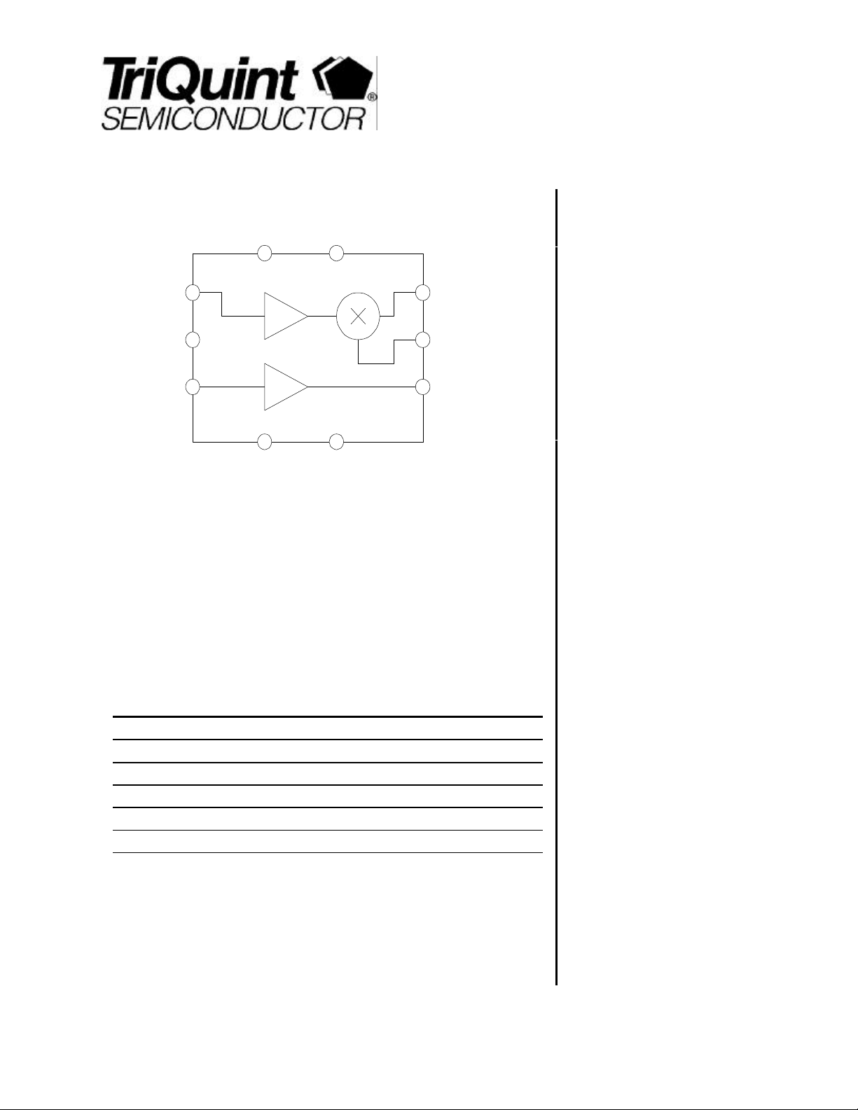
TQ9223C
VDD
Mixer
LO In
Gain
Select
RF In
GND
CNTRL
VDD
Mixer
IF out
Mixer
RF In
LNA
out
LO Tune
Product Description
The TQ9223C 3V RFIC Downconverter is a RF receiver IC front end designed for the
high dynamic range cellular communications standards. The TQ9223C provides a
2.8dB system noise figure for excellent sensitivity, and a good signal range with
-11dB input IP3. Its low current consumption, single +3V operation and small plastic
surface-mount package are ideally suited for cost-competitive, space-limited and
portable applications. The TQ9223C will operate over a RF frequency range of 800
to 1000MHz, and therefore may be used for any of the cellular and cordless
telephony standards.
Electrical Specifications
Parameter Min Typ Max Units
Frequency 800 1000 MHz
Gain 19.0 dB
Noise Figure 2.6 dB
Input 3rd Order Intercept -11.0 dBm
DC supply Current 15.0 mA
Note 1: Test Conditions: Vdd=3.75V, Ta=25C, filter IL=3.0dB, RF=881MHz, LO=966MHz, IF=85MHz,
LO input=-6dBm
1
DATA SHEET
3V Cellular TDMA/AMPS
LNA/mixer Receiver IC
Features
§ +3-V single supply
§ On-chip LO buffer
§ Mixer LO and RF matched to 50Ω
§ Low-cost SO-14 plastic package
§ Gain Select (high/low)
Applications
§ Digital Mobile Phones
§ AMPS Mobile Phones
§ ISM 900MHz
§ Cordless Telephones
§ CDPD terminals
For additional information and latest specifications, see our website: www.triquint.com 1
Page 2
TQ9223C
Data Sheet
Electrical Characteristics
Parameter Conditions Min. Typ/Nom Max. Units
RF Frequency Tuned external match 800 1000 MHz
LO Frequency Tuned external match 500 1300 MHz
IF Frequency Tuned external match 45 300 MHz
LO input level -7 -4 0 dBm
Supply voltage 3.0 3.75 5.5 V
Gain 17.0 19.0 dB
Noise Figure 2.6 3.5 dB
Input 3rd Order Intercept -11.0 dBm
Return Loss Mixer RF input
Mixer LO input
Isolation LO toRF input
Mixer LO to IF after external match
Supply Current 15 mA
Note 1: Test Conditions:, Vdd=3.75V, Ta=25C, filter IL=3.0dB, RF=881MHz, LO=966MHz, IF=85MHz, LO input=-6dBm: unless otherwise specified.
10
10
45
40
dB
dB
dB
dB
Electrical Characteristics-LNA section only
Parameter Conditions Min. Typ/Nom Max. Units
Gain 18.5 dB
Noise Figure 1.8 dB
Input 3rd Order Intercept -6.0 dBm
Reverse Isolation 28.0 dB
Supply Current 5.0 mA
Note 1: Test Conditions:, Vdd=3.75V, Ta=25C, RF=881MHz, external input and output match; unless otherwise specified.
2 For additional information and latest specifications, see our website: www.triquint.com
Page 3
TQ9223C
Data Sheet
Electrical Characteristics- Mixer section only
Parameter Conditions Min. Typ/Nom Max. Units
Conversion Gain 3.5 dB
Noise Figure 12.0 dB
Output 3rd Order Intercept 10.0 dBm
Mixer RF Return Loss 15.0 dB
Mixer LO Return Loss 10.0 dB
LO Input Power -6.0 dBm
LO to IF Isolation 40.0 dB
LO to RF Isolation 5.0 dB
RF to IF Isolation 40.0 dB
Supply Current 4.0 mA
Note 1: Test Conditions:, Vdd=3.75V, Ta=25C, RF=881MHz, LO=966MHz, IF=85MHz, LO input=-6dBm: unless otherwise specified.
Absolute Maximum Ratings
Parameter Value Units
DC Power Supply 8.0 V
RF Input Power +10 dBm
Operating Temperature -40 to 85 C
Storage Temperature -55 to 150 C
For additional information and latest specifications, see our website: www.triquint.com 3
Page 4
TQ9223C
Data Sheet
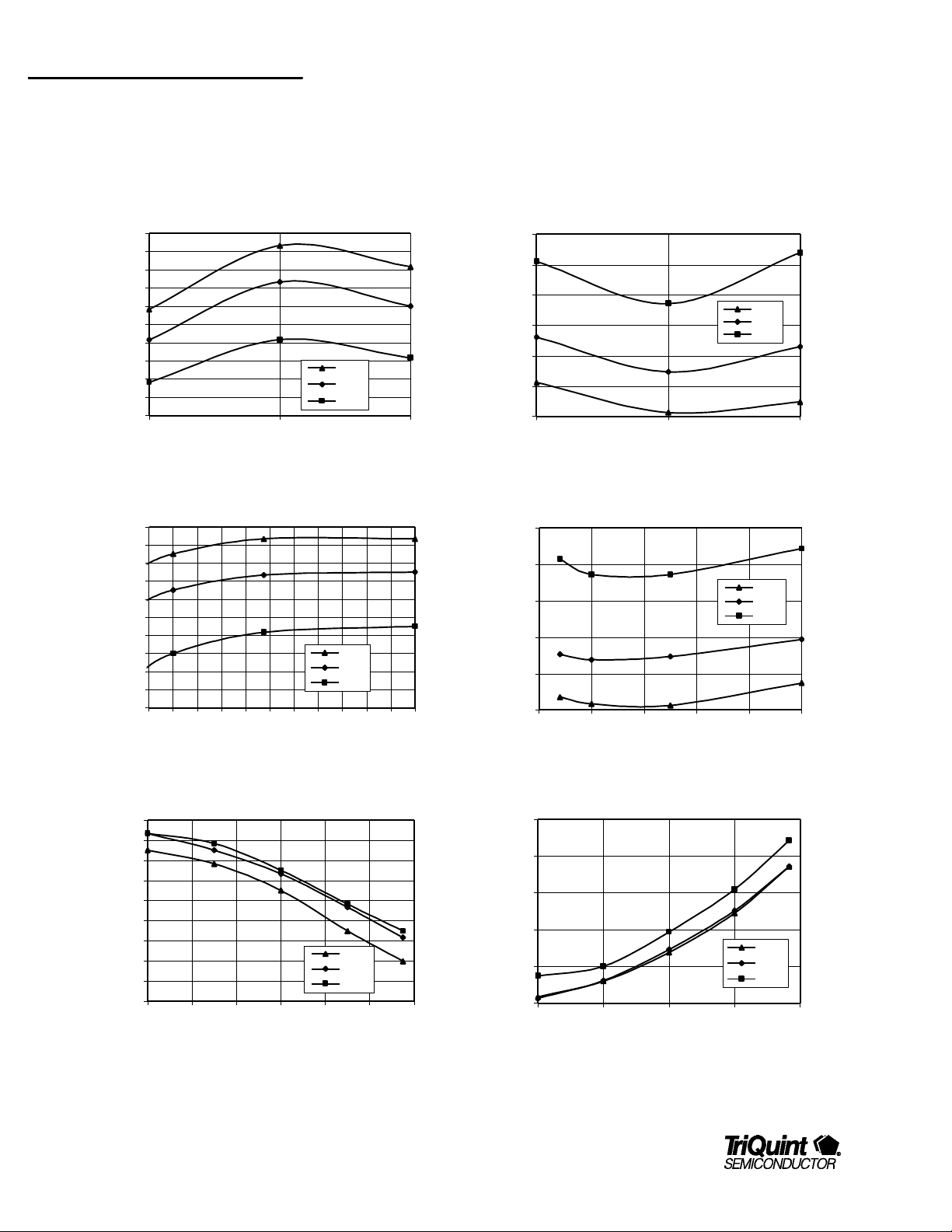
Typical Performance
Test Conditions (Unless Otherwise Specified: Vdd=3.75V, Ta=25C, filter IL=3.0dB, RF=881MHz, LO=966MHz, IF=85MHz, LO input=-6dBm
Conversion Gain v Freq v Temp
24
23
22
21
20
19
18
17
Conversion Gain (dB)
16
15
14
869 881 894
Freq (MHz)
Conversion Gain v Vdd v Temp
24
23
22
21
20
19
18
17
Conversion Gain (dB)
16
15
14
2.8 3 3.2 3.4 3.6 3.8 4 4.2 4.4 4.6 4.8 5
Vdd (Volts)
-30C
+30C
+85C
-30C
+30C
+85C
Noise Figure v Freq v Temp
5
4.5
4
3.5
3
Noise Figure (dB)
2.5
2
869 881 894
Freq (MHz)
Noise Figure v Vdd v Temp
4.5
4
3.5
3
Noise Figure (dB)
2.5
2
2.5 3 3.5 4 4.5 5
Vdd (Volts)
-30C
+30C
+85C
-30C
+30C
+85C
TQ9223 Conversion Gain v Temp v Vdd
24
23
22
21
20
19
18
Conversion Gain (dB)
17
16
15
-30 -10 10 30 50 70 90
Temp (C)
3.0V
3.75V
5.0V
4.5
4
3.5
3
Noise Figure (dB)
2.5
2
-30 0 30 60 90
4 For additional information and latest specifications, see our website: www.triquint.com
Noise Figure v Temp v Vdd
3.0V
3.75V
5.0V
Temp (C)
Page 5

TQ9223C
Data Sheet
IIP3 v Freq v Temp
-4
-6
-8
-10
IIP3 (dBm)
-12
-14
-16
869 881 894
Freq (MHz)
IIP3 v Vdd v Temp
-6
-7
-8
-9
-10
-11
-12
IIP3 (dBm)
-13
-14
-15
-16
2.5 3 3.5 4 4.5 5
Vdd (Volts)
-30C
+30C
+85C
-30C
+30C
+85C
Idd v Vdd v Temp
0.009
0.008
0.007
Idd (A)
0.006
0.005
2.5 3 3.5 4 4.5 5
Vdd (Volts)
-30C
+30C
+85C
IIP3 v Temp v Vdd
-6
-7
-8
-9
-10
-11
-12
IIP3 (dBm)
-13
-14
-15
-16
-30 0 30 60 90
Temp (C)
For additional information and latest specifications, see our website: www.triquint.com 5
3.0V
3.75V
5.0V
Page 6

TQ9223C
Data Sheet
LNA S-Parameters, VDD=3.75V
Freq |S11| <S11 |S21| <S21 |S12| <S12 |S22| <S22
0.100 0.99 -5 2.99 172 0.002 93 0.97 -3
0.200 0.98 -11 2.97 165 0.003 87 0.97 -5
0.300 0.97 -16 2.96 158 0.005 84 0.96 -7
0.400 0.95 -22 2.93 150 0.006 81 0.95 -9
0.500 0.94 -27 2.90 143 0.008 79 0.95 -12
0.600 0.91 -33 2.88 136 0.009 75 0.94 -14
0.700 0.89 -39 2.82 129 0.010 74 0.93 -16
0.800 0.86 -44 2.79 122 0.012 71 0.92 -19
0.900 0.83 -50 2.75 114 0.013 68 0.91 -21
1.000 0.80 -56 2.69 107 0.014 66 0.90 -23
1.100 0.77 -61 2.65 101 0.015 64 0.89 -25
1.200 0.74 -67 2.63 94 0.017 61 0.88 -27
1.300 0.70 -72 2.49 86 0.017 59 0.88 -29
1.400 0.67 -78 2.49 81 0.019 58 0.87 -30
1.500 0.63 -84 2.45 73 0.019 55 0.85 -31
1.600 0.60 -91 2.34 67 0.020 54 0.85 -32
1.700 0.56 -98 2.32 61 0.022 53 0.85 -32
1.800 0.52 -105 2.27 53 0.022 51 0.84 -33
1.900 0.48 -114 2.14 47 0.024 51 0.83 -34
2.000 0.44 -123 2.13 41 0.025 48 0.82 -35
LNA Noise Parameters, Vdd=3.75V
Freq Fmin Γopt (mag) Γopt (ang) Rnoise
0.500 0.618 0.678 10.7 0.59
0.750 0.791 0.656 27.9 0.51
0.900 1.102 0.573 34.3 0.45
1.225 1.311 0.548 48.4 0.42
1.575 1.292 0.522 63.5 0.38
1.900 1.408 0.429 73.6 0.30
6 For additional information and latest specifications, see our website: www.triquint.com
Page 7

TQ9223C
Data Sheet
Mixer S-Parameters, 3.75V
Freq (GHz) RF IN |S11| RF IN <S11 LO IN |S11| LO IN <S11
0.500 0.41 -22 0.12 140
0.600 0.42 -20 0.30 59
0.700 0.42 -23 0.47 28
0.800 0.41 -26 0.57 4
0.900 0.40 -30 0.61 -16
1.000 0.39 -34 0.61 -34
1.100 0.39 -38 0.58 -50
1.200 0.37 -42 0.55 -65
1.300 0.37 -47 0.51 -80
1.400 0.36 -52 0.46 -96
1.500 0.35 -57 0.43 -113
1.600 0.34 -63 0.42 -130
1.700 0.33 -70 0.41 -146
1.800 0.32 -77 0.42 -160
1.900 0.32 -85 0.44 -172
2.000 0.32 -93 0.46 180
Mixer S-Parameters, 3.75V
Freq (GHz) Mixer IF Out |S11| Mixer IF Out <S11
0.045 0.988 0.6
0.085 0.983 1.8
0.125 0.981 2.8
0.165 0.981 3.8
0.205 0.980 4.8
0.255 0.981 6.0
0.295 9.981 6.9
For additional information and latest specifications, see our website: www.triquint.com 7
Page 8

TQ9223C
Data Sheet
Application/Test Circuit
Mixer LO In
Vdd
Gain Select
RF In
R3
R2
C10
R1
L1
C6
C2
C1
C3
C4
1
2
3
4
5
6
7
14
13
12
11
10
9
8
L4
L5
R4
C8
L3
C7
L2
Vdd
C9
Mixer IF Out
Mixer RF In
LNA Out
R5
C5
Vdd
Bill of Material for TQ5121 Receiver Application/Test Circuit
Component Reference Designator Part Number Value Size Manufacturer
Receiver IC U1 TQ9223C SO-14 TriQuint Semiconductor
Capacitor C1, C2, C3, C4, C5, C6 0.01uF 0402
Capacitor C7 1.2pFpF 0402
Capacitor C8 6.0pF 0402
Capacitor C9 15pF 0402
Capacitor C10 2.7pF 0402
Inductor L1 6.8nH 0402
Inductor L2 8.2nH 0402
Inductor L3 33nH 0402
Inductor L4 12nH 0402
Inductor L5 470nH 0402
Resitor R1, R2, R3,R4, R5 10 ohm 0603
8 For additional information and latest specifications, see our website: www.triquint.com
Page 9

TQ9223C
Data Sheet
TQ9223C Product Description
The TQ9223C efficiently integrates a low-noise amplifier and
high-intercept mixer, with performance equal to a discrete
implementation, through use of circuit techniques from
monolithic and discrete design practices. The LNA consists of a
common-source amplifier cascoded to a common-gate amplifier
using a DC-stacked topology. The same DC current flows
through both stages. An external noise match is used to
achieve optimum noise figure. LNA input and output matching
is performed with PC boards microstrip lines or lumped-element
surface-mount components, using simple, well understood
networks.
The mixer is implemented as a “cascode” stage operating like a
dual-gate FET mixer. A common-gate LO buffer provides the
necessary gain to drive the mixer FET gate and establishes a
good input match. The on-chip buffer amplifier allows for direct
connection to a commercial VCO at drive levels down to –6dBm.
An “open collector” IF output allows for flexibility, matching to
various IFs and filter types.
The two topologies efficiently use the supply current for lowpower operation, approximately 10mA with a 3V supply. The
overall circuit provides a distinct performance edge over silicon
monolithic designs in terms of input intercept, noise figure and
gain. Specifically, the circuit was intended for use in the
following applications: cellular (AMPS, GSM, JDC, ETACS,
etc.) and ISM band (902 – 928 MHz)
Operation
Please refer to the test circuit above.
Internally, the downconverter has internal capacitance from Vdd
to ground for RF decoupling of the supply line. This should be
augmented with additional decoupling capacitance: 1000pF
connected externally within 5mm of the package pin. A 10-ohm
series resistor in the Vdd line may also be added (optionally) to
provide some filtering of supply line noise. Connections to
ground should go directly to a low-impedance ground plane.
Therefore, it is recommended that multiple via holes to the
ground plane occur within 2mm on the inside of the package.
LNA Input Interfacing (Pin 6)
The TQ9223C LNA was designed for low-noise operation. It
makes use of an optimum noise-matching network at the input,
not a conjugate match, as would be used for maximum power
transfer. Gamma optimum is referenced from the LNA input into
the noise-match network in series with 50 ohms. The gamma
optimum and the noise parameters for selected frequencies are
shown in the LNA Noise Parameters table.
There are several options for the physical realization of gamma
optimum: a series-shunt inductor microstrip transmission line
network or a series capacitor/shunt inductor. The microstrip
transmission lines can easily be constructed on FR-4 or G-10
circuit boards, using standard design techniques. The lumpedelement components are surface-mount elements designed for
RF use. It is important that the board-level circuit establishes an
impedance of gamma optimum, measured at the solder pad of
pin 6. Proper board design for gamma optimum eliminates the
need for tuning adjustments and produces a low-noise circuit,
which is tolerant of component variations.
LNA Out (Pin 9)
Gain Select (Pin 5)
In a strong signal environment, the LNA can be shut down by
applying 0V to pin 5. The result is that the LNA gain decreases
from a nominal of +18dB to –19dB. The current in the LNA
decreases to 1mA. In addition, the input IP3 for the LNA
increases from –6dBm to +5dBm, and for the downconverter
from –11dBm to –7.5dBm.
Power Supply Connection
The TQ9223C was designed to operate within specifications
over the power supply range of 3.0 to 5.5V. The internal biasing
maintains stable operating points with varying supply voltage.
For additional information and latest specifications, see our website: www.triquint.com 9
The TQ9223C low-noise amplifier requires external output
matching to transform the amplifier's output impedance to the
desired system impedance (typically 50Ω) and to provide a DC
bias path. The recommended output matching circuit is
illustrated in the figure above and consists of a shunt low-Q chip
inductor and a series chip capacitor. The inductor provides a
path for DC current to flow into the amplifier while
simultaneously operating as the first element in the impedance
transforming filter. The series capacitor acts as a block to DC
current and operates as the final element in the impedance
transforming filter.
Page 10

TQ9223C
Data Sheet
A number of inductor/capacitor values can be selected that will
effectively transform the LNA output impedance to the system
impedance. The actual values selected will be governed by the
trade-off between optimum impedance match and maximum IP3
match.
Mixer RF Input (Pin 11)
The mixer RF input is matched close to 50 ohms and is
internally DC-blocked. Pin 11 may be directly connected to the
filter output. The filter must be as close as possible to the mixer
RF input to maintain the proper termination impedance at the
LO frequency. Include a shunt inductor of 33nH at the mixer RF
input to improve the mixer noise performance by providing a
short to ground at the IF frequency. This provides a secondary
benefit of slightly improved input match.
Mixer LO Input (Pin 1)
The mixer LO input is matched close to 50 ohms and is
internally DC-blocked. Pin 1 may be directly connected to the
LO input signal. A level greater than –6dBm is recommended.
Standard VCO outputs of –2dBm work well.
measurement. This “tuning” needs to be done only in design,
not in production.
Mixer IF Interfacing
The mixer IF port is a high-impedance, open-drain output. The
impedance is a few K ohms in parallel with less than 1pF
capacitance. The IF port S-parameters (S11) are listed in the
table over the frequency range of 45MHz to 250MHz. It is
possible to use IFs above and below this range: however, at low
frequencies the noise increases, and at high frequencies the
LO/IF, RF/IF isolation decreases.
The open-drain output permits matching to any chosen filter
impedance. In general, a conjugate impedance match is
recommended on this port to achieve best power gain, noise
figure and output 3rd-order intercept. It is also important to
properly center the tuned circuit at the desired IF. This
maximizes circuit robustness to component tolerances. For
proper mixer operation, pin 14, the open-drain output, must also
be biased to Vdd. A practical matching network, which includes
biasing, is shown.
LO Tuning (Pin 13)
A shunt L on pin 13 resonates with some internal capacitance to
produce a bandpass frequency response of the LO buffer
amplifier. This attenuates noise at +/- one IF frequency away
from the LO frequency. The approximate value of L is
determined by the following equation:
L=1/C (2πf)2, where C=2.2pF
In practice, the value (and/or placement) of L should be
empirically determined for a particular layout, since stray
capacitance on the PCB layout can move the resident frequency
from the expected ideal. The actual value of L should be
adjusted until the buffer response (pin 1-> pin 13) produces a
peak at the LO frequency. A measurement of the response may
be accomplished with a simple coaxial probe “sniffer,” in which
the end is positioned 50 – 100 mils from the inductor at pin 13.
The frequency response of the LO buffer amplifier (pin 13) is
directly measured on the network analyzer as the LO input (pin
1) is swept in frequency. The LO drive level should be set at
approximately the operating level (-6 to -3dBm) for this
10 For additional information and latest specifications, see our website: www.triquint.com
Page 11

Package Pinout
TQ9223C
Data Sheet
Mixer LO input
GND
Mixer Vdd
CNRTL Vdd
Gain Select
LNA RF Input
GND GND
1
2
3
4
5
6
7
14
Mixer IF Output
13
LO Tune
12
GND
11
Mixer RF Input
10
GND
9
LNA Output
8
Pin Descriptions
Pin Name Pin # Description and Usage
Mixer LO IN 1
Mixer Vdd 3 Mixer LO buffer Vdd. Bypass cap required.
CNTRL Vdd 4 LNA gain select control Vdd. Bypass cap required.
Gain Select 5 LNA gain select line. Logic HIGH = high gain, logic LOW = low gain
RF IN 6 LNA RF Input port. Noise matching required. External DC blocking required.
LNA Out 9 LNA Output port. Open drain output requires connection to Vdd and optimal impedance matching.
Mixer RF IN 11
LO Tune 13 LO buffer tuning, inductor to ground.
Mixer IF Out 14 Mixer IF signal port. Open drain output requires connection to Vdd and impedance matching to load.
GND 2,7,8,
10,12
Mixer LO input. Matched to 50Ω. Internally DC blocked.
Mixer RF Input port. Matched to 50Ω. Internally DC blocked.
Ground connection. Keep physically short for stability and performance. Use several via holes immediately adjacent to
the pins down to backside ground plane.
For additional information and latest specifications, see our website: www.triquint.com 11
Page 12

TQ9223C
Data Sheet
Package Type: SO-14 Plastic Package
Dimensions in inches
Additional Information
For latest specifications, additional product information, worldwide sales and distribution locations, and information about TriQuint:
Web: www.triquint.com Tel: (503) 615-9000
Email: info_wireless@tqs.com Fax: (503) 615-8900
For technical questions and additional information on specific applications:
Email: info_wireless@tqs.com
The information provided herein is believed to be reliable; TriQuint assumes no liability for inaccuracies or omissions. TriQuint assumes no responsibility for the use of
this information, and all such information shall be entirely at the user's own risk. Prices and specifications are subject to change without notice. No patent rights or
licenses to any of the circuits described herein are implied or granted to any third party.
TriQuint does not authorize or warrant any TriQuint product for use in life-support devices and/or systems.
Copyright © 1998 TriQuint Semiconductor, Inc. All rights reserved.
Revision C,April 9, 1999
12 For additional information and latest specifications, see our website: www.triquint.com
 Loading...