

Page 1
WIRELESS COMMUNICATIONS DIVISION
TQ9222
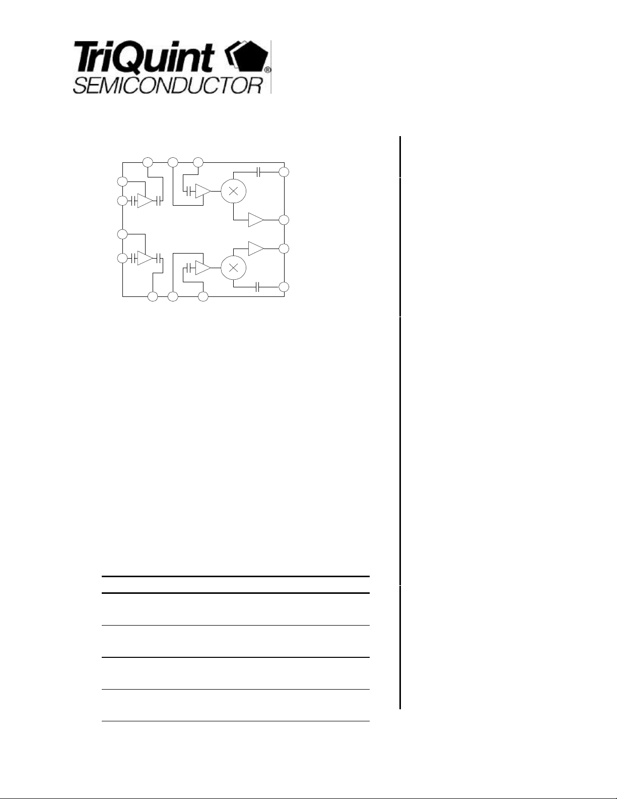
800
Vdd
MXR 1900
Vdd
MXR 800
MXR LO
1900
MXR LO
800
MXR RF
1900
MXR IF
1900
MXR IF
800
MXR RF
800
Vdd LNA
1900
LNA IN
1900
Vdd LNA
800
LNA IN
800
LNA OUT
1900
LNA OUT
Product Description
The TQ9222 is a 3-V, RF receiver IC designed specifically for dual-band TDMA
applications. Its RF performance meets the requirements of products designed to
the IS-136 and GSM standards. The TQ9222 is pin compatible with TQ5121 (cellular
band LNA/Mixer) which enables handset designers to use strategic board platform
strategy.
The TQ9222 contains two separate LNA+Mixer circuits to handle both the 800 MHz
cellular band and the 1900 MHz PCS band. The mixers use a high-side LO
frequency, with the IF covering a range of 70-140 MHz. IF frequencies below 120
MHz are possible due to the ½-IF spurious signal rejection in the 1900 MHz
LNA+Mixer. The IF outputs are designed for use of a common IF frequency. Most
RF ports are internally matched to 50Ω, greatly simplifying the design and keeping
the number of external components to a minimum. Separate supply voltage
connections provide the required flexibility for dual-band operation. The TQ9222
achieves good RF performance with low current consumption, supporting long
standby times in portable applications. Coupled with the very small QSOP-24
package, the part is ideally suited for dual-band mobile phones.
DATA SHEET
Dual-Band TDMA
LNA/Downconverter IC
Features
§ Pin compatible with TQ5121
§ Single 3 V operation
§ Low-current operation
§ Low-frequency IF capability
§ Excellent ½ IF rejection
§ IF output combining
§ 50 Ω matched inputs (most ports)
§ QSOP-24 plastic package
Applications
Electrical Specifications
1
§ IS-136 dual-band Mobile Phones
§ Tri-Mode Phones
Parameter Typ Units
Gain 800 band
1900 band
Noise Figure 800 band
1900 band
Input 3rd Order Intercept 800 band
1900 band
DC supply Current 800 band
1900 band
Note 1: Test Conditions: Vdd=2.8V, Ta=25C, filter IL=2.5dB, RF1=881MHz, RF 2=1960MHz,
LO1=991MHz, LO2= 2070MHz, IF=110MHz, LO Input=-7dBm; unless otherwise specified
17.5
17.5
2.7
3.0
-9.0
-9.0
10.0
22.0
MHz
MHz
dB
dB
dBm
dBm
mA
mA
For additional information and latest specifications, see our website: www.triquint.com 1
§ GSM dual-band Mobile Phones
§ Wireless local loop
Page 2
TQ9222
Data Sheet
Electrical Characteristics
Parameter Conditions Min. Typ/Nom Max. Units
RF Frequency Cellular band
PCS band
LO Frequency Cellular band
PCS band
IF Frequency Cellular band 85 140 MHz
LO input level -7 -4 0 dBm
Supply voltage 2.7 2.8 3.0 V
Gain Cellular band
PCS band
Gain Variation vs. Temp. -40 to 85C -2.0 +2.0 dB
Noise Figure Cellular band
PCS band
Input 3rd Order Intercept Cellular band
PCS band
Return Loss
Cellular and PCS band
Isolation
Cellular and PCS bands
IF Output Impedance
Cellular and PCS band
Supply Current Cellular band
Note 1: Test Conditions: Vdd=2.8V, Ta=25C, filter IL=2.5dB, RF1=881MHz, RF2=1960MHz, LO1=991MHz, LO2= 2070MHz, IF=110MHz, LO Input=-7dBm; unless
otherwise specified
LNA input – external match
LNA output
Mixer RF input
Mixer LO input
LO to LNA in
LO to IF; after IF match
RF to IF; after IF match
Vdd = 2.8V; “ON”
Vdd = 0V; “OFF”
PCS band
Absolute Maximum Ratings
869
1930
950
2010
16.0
16.0
-11.0
-11.0
10
10
10
10
40
17.5
17.5
2.7
3.0
-9.0
-9.0
40
40
500
<50
10
22
894
1990
1040
2140
3.5
3.5
13 mA
MHz
MHz
MHz
MHz
dB
dB
dB
dB
dBm
dBm
dB
dB
dB
dB
dB
dB
dB
Ohm
Ohm
mA
Parameter Value Units
DC Power Supply 5.0 V
Power Dissipation 500 mW
Operating Temperature -40 to 85 C
Storage Temperature -60 to 150 C
Signal level on inputs/outputs +20 dBm
Voltage to any non supply pin -.3 to +.3 V
2 For additional information and latest specifications, see our website: www.triquint.com
Page 3
TQ9222
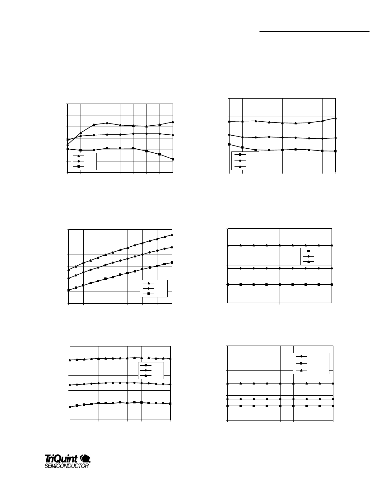
Conversion Gain vs. Vdd vs. Temp
Noise Figure vs. Freq vs. Temp
Data Sheet
Typical Performance
Test Conditions: TQ9222 Low Band (Unless Otherwise Specified): Vdd=2.8V, Ta=25C, filter IL=2.5dB, RF=881MHz, LO=991MHz, IF=110MHz, LO input=-7dBm
Conversion Gain vs. Freq vs. Temp
*Note: rolloff at -40C and +85C due to change in SAW filter Fc over temperature
20
5
19
18
17
Gain (dB)
16
15
14
869 872 875 878 881 884 887 890 893
20
19
18
17
Gain (dB)
16
15
14
2.5 2.6 2.7 2.8 2.9 3 3.1 3.2
-40C
+25C
+85C
Freq (MHz)
-40C
+25C
+85C
Vdd (volts)
4
3
Noise Figure (dB)
2
1
869 872 875 878 881 884 887 890 893
11
10
9
Idd (mA)
8
7
869 875 881 887 893
-40C
+25C
+85C
Freq (MHz)
Idd vs. Freq vs. Temp
-40 C
+25 C
+85 C
Freq (MHz)
-7
-8
-9
-10
IIP3 (dBm)
-11
-12
IIP3 vs. Vdd vs. Temp
-40C
+25C
+85C
2.5 2.6 2.7 2.8 2.9 3 3.1 3.2
Vdd (volts)
For additional information and latest specifications, see our website: www.triquint.com 3
Idd vs. Freq vs. Vdd
11
Vdd= 2.8v
Vdd= 2.7v
10
Idd (mA)
9
8
869 872 875 878 881 884 887 890 893
Freq (MHz)
Vdd= 3.0v
Page 4

TQ9222
Data Sheet
Typical Performance:
Test Conditions: TQ9222 High Band (Unless Otherwise Specified): Vdd=2.8V, Ta=25C, filter IL=2.5dB, RF=1960MHz, LO=2070MHz, IF=110MHz, LO input=-7dBm
Conversion Gain vs. Freq. vs. Temp.
20
19
18
CG (dB)
17
16
15
1930 1940 1950 1960 1970 1980 1990
Conversion Gain vs. Vdd vs. TEMP
21
20
19
18
17
CG (dB)
16
15
14
2.5 2.6 2.7 2.8 2.9 3 3.1 3.2
Freq (MHz)
Vdd (v)
-40 C
+25 C
+85 C
-40 C
+25 C
+85 C
Noise Figure vs. Freq. vs. Temp.
5
4
3
NF (dB)
2
1
1930 1940 1950 1960 1970 1980 1990
Freq (MHz)
Idd vs Freq. vs Temp.
26
24
22
Idd (mA)
20
18
1930 1940 1950 1960 1970 1980 1990
Freq (MHz)
-40 C
+85 C
+25 C
-40 C
+25 C
+85 C
IIP3 vs. Vdd vs. TEMP
-7
-8
-9
-10
IIP3 (dBm)
-11
-12
-13
2.5 2.6 2.7 2.8 2.9 3 3.1 3.2
Vdd (v)
-40 C
+25 C
+85 C
26
24
22
Idd (mA)
20
18
1930 1940 1950 1960 1970 1980 1990
4 For additional information and latest specifications, see our website: www.triquint.com
Idd vs Freq. vs Vdd
Vdd= 2.7v
Vdd= 2.8v
Vdd= 3.0v
Freq (MHz)
Page 5
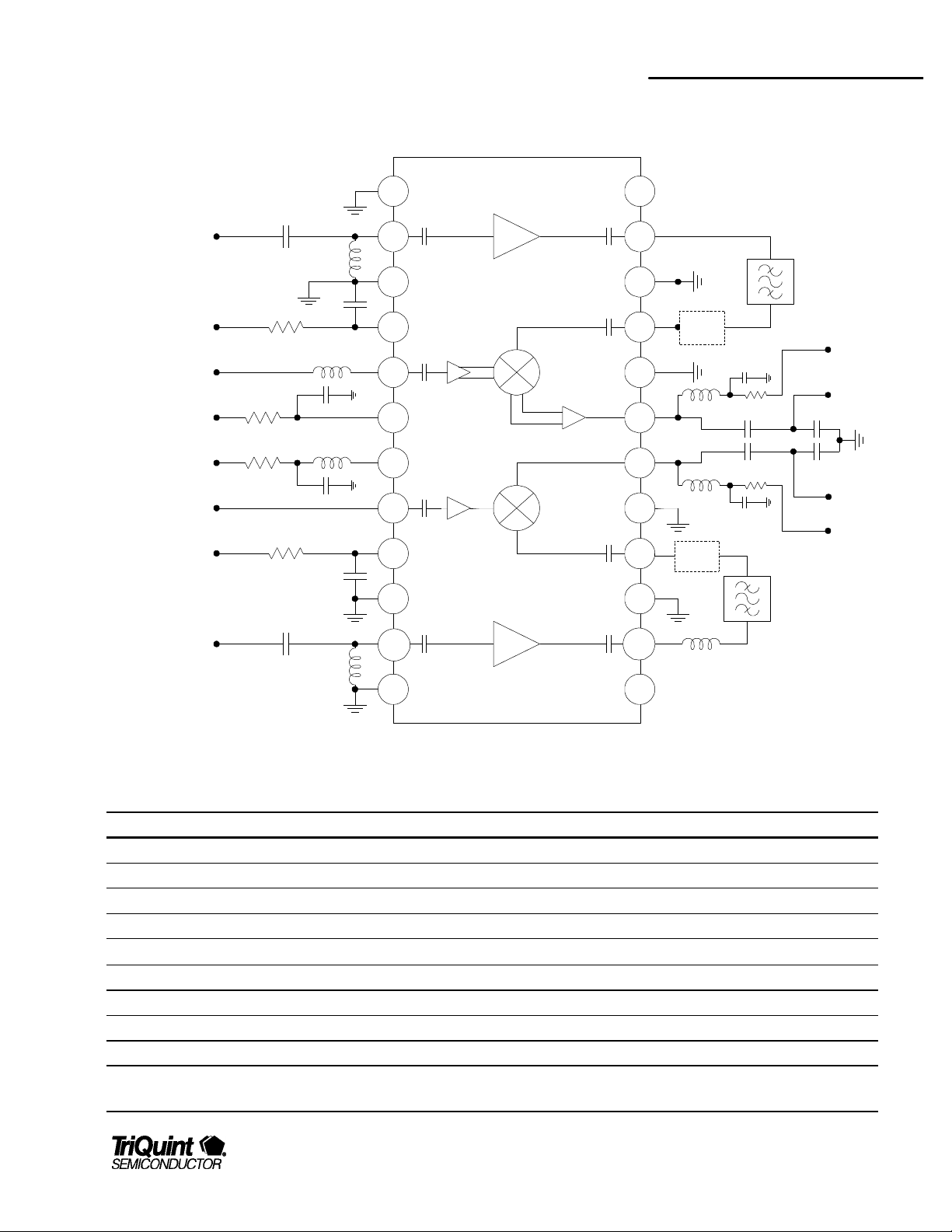
Application/Test circuit
TQ9222
Data Sheet
LNA in B
V LNA B
LO in B
V MX B
V MX A
LO in A
V LNA A
LNA in A
R4
R2
R5
R1
C1
C6
C4
C3
C2
1
2
L4
3
C5
L3
L2
L1
4
5
6
7
8
9
10
11
12
24
23
22
2
21
20
19
18
17
2
16
15
14
13
N2
L6
L5
L8
N1
1
C7
R6
C8
C11
R3
C10
1
F2
V IF B
IF out B
C9
C12
IF out A
V IF A
F1
TQ9222
Bill of Material for TQ9222 Receiver Application/Test Circuit
Component Reference Designator Part Number Value Size Manufacturer
Receiver IC U1 TQ9222 QSOP-24 TriQuint Semiconductor
Capacitor C1 1.2pF 0603
Capacitor C2, C3, C4, C5 1000pF 0603
Capacitor C6 1.5pF 0603
Capacitor C7, C10
.01µF
Capacitor C9 4.7pF 0603
Capacitor C8, C11 12pF, 10pF 0603
Capacitor C12 8.2pF 0603
Capacitor C13 1.5pF 0603
Capacitor C14, C15 (filter
0.5pF 0603
dependent)
For additional information and latest specifications, see our website: www.triquint.com 5
0603
Page 6

TQ9222
Data Sheet
Flter F1 869-894MHz
Filter F2 1930-1990MHz
Inductor L1 10nH 0603
Inductor L2 8.2nH 0603
Inductor L3 6.8nH 0603
Inductor L4 2.7nH 0603
Inductor L5, L6 180nH 0603
Inductor L7 (filter dpendent) 2.7nH 0603
Inductor L8 10nH 0402
Inductor L9 (filter dependent) 2.2nH 0603
Resistor R1-6 (power supply
only)
10 Ohm 0603
C13
N1
N1
L7
C14
C15
2
2
1
1
N2
L9
1
1
*
OPTIONAL FILTER OUTPUT NETWORKS, DEPENDING UPON FILTER TYPE, BOARD
denotes networks used for data sheet parameters
*
LAYOUT, AND IF FREQUENCY
*
6 For additional information and latest specifications, see our website: www.triquint.com
Page 7

Introduction
Vdd
The TQ9222 3V RFIC Downconverter is designed specifically
for dual-band TDMA applications. The TQ9222 contains two
separate LNA+Mixer circuits to handle both the 800 MHz
cellular band and the 1900 MHz PCS band. The IF frequency
range covers 70 to 140 MHz. Most of the ports are internally
matched to 50 Ω simplifying the design and keeping the number
of external components to a minimum. Separate supply voltage
connections provide the required flexibility for dual-band
operation.
Operation: Please refer to the applications test circuit above.
General Description
Low Noise Amplifier (LNA)
TQ9222
Data Sheet
gate LO buffer provides a good input match, and supplies the
voltage gain necessary to drive the mixer FET gate. The "open-
drain " IF output allows for flexibility in matching to various IF
frequencies and filter impedances (see Fig. 2).
Fig 2. Cellular Band Mixer
Mixer LO
Input
LO Bias and
Tuning
Mixer RF
Input
Mixer IF
Output
The LNA sections of the TQ9222 consist of two cascaded
common source FETs (see Fig 1). Each LNA is designed to
operate on supply voltages from 3V to 5V. The main differences
between the high and low band LNAs are the bias circuits. The
source terminal of the first stage has to be grounded very close
to the pin (pin 1 for PCS band and pin 12 for cellular band). This
will avoid a significant gain reduction due to degeneration. The
LNA requires a matching circuit on the input to provide a good
noise, gain and return loss performance. The output is close to
50 Ω for direct connection to a 50 Ω image stripping filter.
Fig 1. TQ9222
Simplified
Schematic of
LNA Section
LNA
in
BIAS
LOAD
LNA
out
BIAS
Fig 1. LNA Sections
PCS Band Mixer
The PCS band mixer section of the TQ9222 is a balanced
mixer with a single ended output. This balanced mixer topology
minimizes the LO leakage out of the RF and IF ports thereby
giving excellent LO suppression (see Fig. 3)
Mixer LO
Input
Mixer RF
Input
Vdd
Mixer IF
Output
Fig 3. PCS Band Mixer
Low Noise Amplifier Application
Cellular Band Mixer
The cellular band mixer of the TQ9222 is implemented by a
common source depletion FET. The mixer is designed to
operate on supply voltages from 3V to 5V. An on-chip buffer
amplifier simplifies direct connection of the LO input to a
commercial VCO at drive levels down to -7dBm. The common-
For additional information and latest specifications, see our website: www.triquint.com 7
To obtain the best possible combination of performance and
flexibility, the high and low band LNAs were designed to be
used with off-chip input impedance matching. Based on the
system requirements, the designer can make several
performance trade-offs and select the best impedance match for
the particular application.
Page 8

TQ9222
F
−
1
Data Sheet
LNA Input Match
The input matching network primarily determines the noise and
gain performance. Fig 4 shows a suggested input match for the
high band. The low band uses a series 1.2pF capacitor and a
shunt 10nH inductor.
1.2pF
RF
IN
Note: These values assume ideal components and neglect board parasitics.
The discrepancy between these values and those of the typical application
circuit are the board and component parasitics.
10nH
Fig 4. LNA Input Match
The LNA gain, noise figure and input return loss are a function
of the source impedance (Zs), or reflection coefficient (Γs),
presented to the input pin. Highest gain and lowest return loss
occur when Γs is equal to the complex conjugate of the LNA
input impedance. A different source reflection coefficient, Γ
which is experimentally determined, will provide the lowest
possible noise figure, F
min
.
Pin 2
opt
Designing the input matching network involves a compromise
between optimum noise performance and best input return loss.
For example, when the TQ9222 LNA is matched for optimum
noise figure (1.35dB @ 880 MHz, and 1.45dB @ 1960 MHz),
the input return loss is only about 4dB. On the other hand,
when the LNA is matched for best return loss, the LNA noise
figure is approximately 1.95dB @ 881 MHz and 2.14dB @
1960MHz (see Table 1.)
Low Band
Freq |Γopt| <Γopt Fmin Rn
(MHz) (dB)
835 0.678 33 1.34 61.6
850 0.655 34 1.38 61.1
865 0.652 36 1.36 61.2
880 0.652 38 1.35 60.9
895 0.649 38 1.36 61.3
910 0.659 40 1.35 61.2
925 0.687 41 65.6
High Band
Freq |Γopt| <Γopt Fmin Rn
,
(MHz) (dB)
1860 0.557 51 1.44 31.1
1960 0.555 54 1.45 31.7
2060 0.532 59 1.61 29.0
1.35
(Ω)
(Ω)
Table 1. Noise Parameters
The noise resistance, Rn, provides an indication of the sensitivity
of the noise performance to changes in Γs as seen by the LNA
input.
2
−
2 2
s
( )
F F
LNA MIN
= + ⋅
R
N opt S
4
Z
0
Γ Γ
opt
+ ⋅ −
1 1
Γ Γ
Components such as filters and mixers placed after the LNA
degrade the overall system noise figure according to the
following equation:
F F
SYSTEM LNA
= +
where F
LNA
and G
2
G
LNA
represent the linear noise factor and gain
LNA
of the LNA and F2 is the noise factor of the next stage. Thus, the
system noise figure depends on the highest gain and minimum
noise figure of the LNA.
LNA Output Match
The output impedance of the high and low band LNAs, were
designed to interface directly with 50Ω terminations. This
internal match serves to reduce the number of external
components required at this port. An additional benefit accrues
as an improvement in IP3 performance, return loss and power
gain.
Low Band LNA Output
The output of the low band LNA will most often be connected to
an image stripping filter. Depending on the filter type, additional
components might be needed to present a better match to the
LNA output. The TQ9222 general applications circuit shows a
TOYOCOM (637-881A) saw filter for the low band. A series
inductor “L8” of 10nH is added to the filter input to improve the
match. This series inductor also smoothes out excessive ripple
in the filter passband improving the overall performance of the
circuit.
8 For additional information and latest specifications, see our website: www.triquint.com
Page 9

TQ9222
TQ9222 Mixer
Data Sheet
High Band LNA Output
The output of the high band LNA can also be connected directly
to the image stripping filter. However, it has been found that
some SAW filters can cause low image rejection in the circuit as
a whole, even as their individual characteristics show rejection
of 30-40dB. It appears that the very low impedance of the SAW
filter at the image frequency can be reflected back to the LNA
output pin, lessening the effectiveness of the ground, and
leaking into the mixer input.
The optimum solution would be to include a 1/4 wavelength
transmission line between the LNA output and SAW input in
order to invert the impedance. However, a more compact
solution is to bridge a small capacitor across a much shorter
transmission line, giving a much longer effective length. (refer to
Fig 9). It may also be possible to entirely use lumped
components to accomplish the same. On the evaluation board,
the transmission line is looped to that the capacitor can be
varied in its positioning, thus facilitating tuning.
Low Band Mixer: LO Port
evaluation board, a small inductance “L8” is added on the SAW
output to compensate. With certain longer line lengths it is
possible to omit “L8”.
Low Band LO Buffer Tune
While the broadband input match of the LO buffer amplifier
makes interfacing easy, the broadband gain means that thermal
and induced noise at other frequencies can be amplified and
injected directly into the LO port of the mixer. Noise at the IF
frequency, and at LO +/- IF will be downconverted and emerge
at the IF port, degrading the downconverter noise figure.
As indicated on the diagram of Fig 5, in order to test the LO
response to these spurious signals, a two-tone signal was
injected into the LO port with the RF port terminated in 50Ω.
One signal generator is set to the LO frequency at its normal LO
drive level usually (-7 dBm). The second signal generator
(spurious signal) is set to the LO +/- the IF frequency. The
combined input power at mixer LO port has to be less than -50
dBm. The results shown in Table 2 indicate a good suppression
of the interfering signals.
As mentioned earlier, a common gate buffer amplifier is
positioned between the LO port and the mixer FET gate in order
to provide a good impedance to the VCO and to allow operation
at lower LO drive levels. The buffer amplifier provides the
voltage gain needed to drive the gate of the mixer FET while
consuming very little current (approximately 1.5mA).
Because of the broadband 50Ω input impedance of the buffer
amplifier and the internal DC blocking capacitor, the user’s VCO
can be directly connected to the LO input via a 50Ω line with no
additional components.
Low Band Mixer Input
Although the low band mixer input port has been designed with
a 50Ω impedance, it has been found that LO leakage out
through the pin can in some cases reflect off the SAW filter and
travel back to the mixer input out of phase, causing some
degradation in conversion gain and system noise figure.
Sensitivity to the phenomena depends on the particular filter
model and SAW-mixer transmission line length. On the
50 ohm
SIG 1:
FLO
RF IF
LO
Directional
+
FLO +/- IF
Spectrum
Analyzer
Coupler
SIG 2:
Fig. 5 LO Spurious Response Diagram
LO/Spurious
(MHz)
Mixer LO Port
Input Power
991/1101 -57 -71.7
991/1101 -58.9 -71.8
Table 2. LO Spurious Response Data
C/V
(dB)
For additional information and latest specifications, see our website: www.triquint.com 9
Page 10

TQ9222
Ground
Data Sheet
Calculation of Nominal L Value
The node between the LO buffer amplifier and the mixer FET is
brought out to Pin 7 (L_tune) and connected to a shunt inductor
to AC ground. This inductor is selected to resonate with internal
capacitance at the L0 frequency in order to suppress out-ofband gain and improve noise performance.
The internal capacitance of the LO amplifier output plus the
stray capacitance on the board surrounding Pin 7 is
approximately 1.8 pF. The inductor is selected to resonate with
the total capacitance at the LO frequency using the following
equation:
L
1
= ⋅ =
C f
2
Π
( )
where C pF
, .
2
15
but must be confirmed with measurements on a board
approximating the final layout.
Measuring the LO Frequency Response
The frequency response of the LO driver amplifier can be
measured using a semi-rigid probe (see Fig. 6) and a network
analyzer.
Connect port 1 to the LO input (Pin 8) of the TQ9222 with the
source power set to deliver -7 dBm. Connect the coaxial probe
to Port 2 and place the probe tip approximately 0.1 inch away
from either Pin 7 or the inductor.
Network
Analyzer
Port 2
Port 1
7
Probe
8
TQ9222
If the calculated shunt inductor (L2) is not a standard value, the
AC ground, implemented with C3, can be slide along the
transmission line to adjust for the right inductance (see Fig 7).
Once this is completed, the peak of the response should be
centered at the center of the LO frequency band.
7
TQ9222
Placement of inductor
will adjust between
standard values
Fig 7. Adjusting AC Ground
Mixer IF Port
The Mixer IF output is an "open-drain" configuration, allowing for
flexibility in efficient matching to various filter types and at
various IF frequencies.
For evaluation of the LNA and mixer, it is usually necessary to
impedance match the IF port to the 50Ω test systems. When
verifying or adjusting the matching circuit on the prototype circuit
board, the LO drive should be injected at pin 8 for the Low Band
and pin 5 for the High Band at the nominal power level of -7
dBm, since the LO level does have an impact on the IF port
impedance.
There are several networks that can be used to properly match
the IF port to the SAW or crystal IF filter. The mixer supply
voltage is applied through the IF port, so the matching circuit
topology must contain either an RF choke or shunt inductor. An
extra DC blocking capacitor is not necessary if the output will be
attached directly to a SAW or crystal bandpass filters.
-30
-32
-34
-36
-38
S21 (dB)
-40
-42
1000
Frequency (MHz)
1100 1200900800700
Fig 6. LO Buffer Amplifier Tuning
shunt L, series C, shunt C, is the simplest and requires the
fewest components. The only difference with the high band is
the series capacitor value of 10pF as opposed to 8.2pF. DC
current can be easily injected through the shunt inductor and the
series C provides a DC block, if needed. The shunt C, is used
to reduce the LO leakage.
10 For additional information and latest specifications, see our website: www.triquint.com
Figure 8 shows the IF matching network for the low band. A
Page 11

TQ9222
10pF
700 mils from pin
Data Sheet
10
Mx IF
out
Vdd
Ω
Pin 14
180nH
Note: These values assume ideal components and neglect board parasitics.
The discrepancy between these values and those of the typical application
circuit are the board and component parasitics
8.2pF
0.01uF
Fig. 8 Suggested IF Match
Half-IF Application
When the intermediate frequency is less than twice the
bandwidth of the receiver, Half-IF intermodulation spurs will fall
within the frequency of operation. The image filter and mixer are
the main circuit blocks that influence Half-IF spur suppression.
However, it was shown experimentally that the preselector filter
plays an important role as well in suppressing half-IF and image
spurious signals. The preselector filter eliminates out of band
spurs that could get amplified and degrade the performance.
A narrow band pass filter and a high IF frequency are best to
eliminate Half-IF problems. The other major contribution is mixer
balance which is affected by two factors. First, the LO signal that
leaks into the mixer inputs via parasitics. The second major
contribution is the source impedance presented at the mixer RF
input port. Depending on the board layout, the optimum mixer
source impedance may shift which will degrade the Half-IF
performance.
It is possible to optimize mixer source impedance for Half-IF
rejection at the LO frequency only. This will avoid affecting the
desired signal to a large degree. Experience with the TQ9222,
has shown that optimum mixer source impedance results in a
significant mismatch causing gain reduction. Therefore, a tradeoff has to be made between optimum Half-IF performance and
conversion gain.
The standard TQ9222 evaluation board uses a Toko TDFM1B1960L-11 dielectric filter in the high band. It was found that an Lnetwork, comprised of a series 1.8 nH inductor and a shunt 1.8
pF capacitor on the mixer input, produces the best Half-IF
rejection and conversion gain. To a lesser extent, it was found
that the length of the transmission line in the filter input also has
an effect on Half-IF performance.
to filter input
23
TQ9222
22
1.8pF
21
1.8nH
Fig. 9 Image and Half-IF circuit
Note that if the final board layout is significantly different from
our evaluation board, the network shown will only be useful as a
guideline for development or to show what performance is
possible with the TQ9222. A SAW filter will probably require a
totally different type of network; and network component values
vary widely between SAW filter models.
Usually only a portion of the frequency band will be of concern
for half-IF interference. It will depend on the injection mode of
the LO signal and the IF frequency being used. For example If
the LO is a high side injection such as the case of the TQ9222
and the IF = 110 MHz then (theoretically) we worry about the
first 5 MHz of the band (1930-1935) only if we have ideal filters.
Unfortunately most of the image stripping filters roll-off around
2000 MHz or higher hence the need to optimize performance up
to 1945 MHz. The opposite occurs for low side LO.
Since the frequency response of the preselector and image
stripping filter help the performance at the high end of the band,
the TQ9222 was tuned to give good half-IF rejection at the low
end of the band over a wide temperature range (-40 °C to +85
°C). That was accomplished with a Pi-network* (between the
filter output and the mixer input) comprise of a series L = 2.2
nH, shunt C = 1.0 and 0.5 pF. As expected this tuning network
degraded the half-IF performance from 1970 to 1990 MHz
specially at the extremes temperatures. However, once the
For additional information and latest specifications, see our website: www.triquint.com 11
Page 12

TQ9222
Data Sheet
downconverter was tested with the preselector filter, the
performance improved significantly. The results are shown in
Table 3.
Freq Temp Half-IF
(MHz) (°C) (dB)
1930 -40 70.30
1940 -40 71.72
1980 +85 72.46
1990 +85 70.21
Table 3. TQ9222 Performance with Preselector Filter (IF = 110
MHz, PLO = -7 dBm, Vdd = 2.8v)
The preselector filter not only improved the half-IF performance
but also the image rejection up to 70 dB, RF to IF isolation up to
33dB, and LO to IF isolation up to 43dB.
*This is one of many different circuit topologies that could give similar results.
The circuit selected that gives the best performance will depend on the PCB
layout.
12 For additional information and latest specifications, see our website: www.triquint.com
Page 13

Package Pinout
TQ9222
Data Sheet
LNA GND 1900
LNA IN 1900
GND
Vdd LNA 1900
MXR LO 1900
Vdd MXR 1900
Vdd MXR 800
MXR LO 800
Vdd LNA 800
GND
LNA IN 800
LNA GND 800
1
2
3
4
5
6
7
8
9
10
11
12
24
N/C
23
LNA OUT 1900
22
GND
21
MXR RF 1900
20
IF TUNE
19
MXR IF 1900
18
MXR IF 800
17
GND
16
MXR RF 800
15
GND
14
LNA OUT 800
13
N/C
TQ9222
Pin Descriptions
Pin Name Pin # Description and Usage
LNA GND 1900 1 High-band LNA first-stage ground connection. Direct connection to ground.
LNA IN 1900 2
Vdd LNA 1900 4 High-band LNA supply voltage. Local bypass cap required.
MXR LO 1900 5
Vdd MXR 1900 6 High-band Mixer LO buffer supply voltage. Local bypass cap required.
Vdd MXR 800 7 Low-band Mixer LO buffer supply voltage. Local bypass cap required.
MXR LO 800 8
Vdd LNA 800 9 Low-band LNA supply voltage. Local bypass cap required.
LNA IN 800 11
GND LNA 800 12 Low-band LNA first-stage ground connection. Connection to ground.
N/C 13 Open pin. No connection.
LNA OUT 800 14
High-band LNA input. DC blocked, requires external matching elements for noise match and match to 50Ω.
High-band Mixer LO input. Internally DC blocked. L3 required for 50Ω match.
Low-band Mixer LO input. Matched to 50Ω. Internally DC blocked.
Low-band LNA input. DC blocked, requires external matching elements for noise match and match to 50Ω.
Low-band LNA output. Matched to 50Ω. Internally DC blocked.
For additional information and latest specifications, see our website: www.triquint.com 13
Page 14

TQ9222
Data Sheet
MXR RF 800 16
MXR IF 800 18 Low-band Mixer IF output. Open-drain output. Connection to Vdd required, external matching is required.
MXR IF 1900 19 High-band Mixer IF output. Open-drain ouput. Connection to Vdd required, external matching is required.
IF TUNE 20 Half-IF tuning inductor to ground for optimum half-IF performance in the high-band mixer.
MXR RF 1900 21
LNA OUT 1900 23
N/C 24 Open pin. No connection.
GND 3, 10, 15,
17, 22
Low-band Mixer RF input. Matched to 50Ω, internally DC blocked.
High-band Mixer RF input. Matched to 50Ω, internally DC blocked.
High-band LNA output. Matched to 50Ω, internally DC blocked.
Ground connection. Use several via holes immediately adjacent to the pins down to backside ground plane.
14 For additional information and latest specifications, see our website: www.triquint.com
Page 15

Package Type: Power QSOP-24 plastic Package
TQ9222
Data Sheet
For additional information and latest specifications, see our website: www.triquint.com 15
Page 16

TQ9222
Data Sheet
Additional Information
For latest specifications, additional product information, worldwide sales and distribution locations, and information about TriQuint:
Web: www.triquint.com Tel: (503) 615-9000
Email: info_wireless@tqs.com Fax: (503) 615-8900
For technical questions and additional information on specific applications:
Email: info_wireless@tqs.com
The information provided herein is believed to be reliable; TriQuint assumes no liability for inaccuracies or omissions. TriQuint assumes no responsibility for the use of
this information, and all such information shall be entirely at the user's own risk. Prices and specifications are subject to change without notice. No patent rights or
licenses to any of the circuits described herein are implied or granted to any third party.
TriQuint does not authorize or warrant any TriQuint product for use in life-support devices and/or systems.
Copyright © 1998 TriQuint Semiconductor, Inc. All rights reserved.
Revision B, December 1, 1998
16 For additional information and latest specifications, see our website: www.triquint.com
 Loading...