

Page 1
WIRELESS COMMUNICATIONS DIVISION
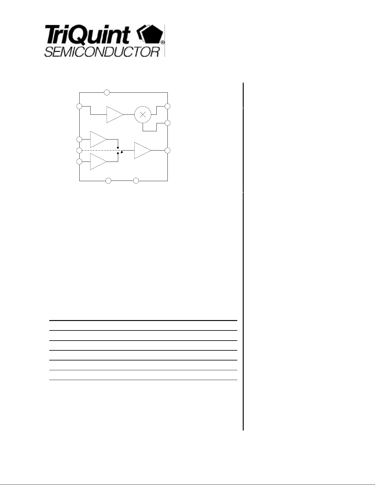
TQ9203
VDD
Mixer
LO In
LNA
IN0
Select
LNA
IN1
GND
LO Tune
Mixer
IF out
Mixer
RF In
LNA
out
Product Description
The TQ9203 RFIC Downconverter is a multifunction RF front end designed for the
high dynamic range cellular communications standards. The design of the TQ9203
provides a 2.5dB system noise figure for excellent sensitivity, and a good signal
range with –10dBm input IP3. Its low current consumption, single +5V operation and
small, plastic surface-mount package are ideally suited for cost-competitive, spacelimited and portable applications. In addition, two selectable RF inputs simplify
implementation of “antenna diversity” in applications such as CDPD. The TQ9203 is
specified over a RF frequency range of 800 to 1000MHz, and therefore may be used
for any of the cellular and cordless telephony standards.
DATA SHEET
Low-Current Cellular
Band Downconverter IC
Features
§ +5-V single supply
§ Internal buffer amplifier on mixer
LO port
§ On-chip matching to 50Ω
§ Two selectable RF inputs
§ Low-cost SO-14 plastic package
§ 21dB system gain
§ -10dBm typical input intercept point
§ 2.5dB typ. system noise figure
§ 10.5mA typ. operating current
Electrical Specifications
Parameter Min Typ Max Units
Frequency 800 1000 MHz
Gain 21.0 dB
Noise Figure 2.5 dB
Input 3rd Order Intercept -10.0 dBm
DC supply Current 10.5 mA
Note 1. Test Conditions: Vdd=5V, Ta=25C, filter IL=3.0dB, RF=881MHz, LO=966MHz, IF=85MHz,
LO input=-6dBm
2. Specified with external noise-matching circuit elements, with image-stripping BPF IL=3dB
3. Frequency separation of the two signals is 500KHz; BPF IL=3dB
1
Applications
§ Cellular Communications
§ Spread-Spectrum Receivers
§ Cordless Phones
Electrical Characteristics
For additional information and latest specifications, see our website: www.triquint.com 1
Page 2

TQ9203
Data Sheet
Parameter Conditions Min. Typ/Nom Max. Units
RF Frequency Tuned external match 800 1000 MHz
LO Frequency Tuned external match 700 1300 MHz
IF Frequency Tuned external match 30 300 MHz
LO input level -6 dBm
Supply voltage 4.5 5.0 5.5 V
Gain (LNA IN1)
Gain (LNA IN0)
Noise Figure LNA IN0 Pin; SSB
Input 3rd Order Intercept Frequency Sep. = 500KHz -10.0 dBm
Return Loss Mixer RF input
Supply Current 10.5 12 mA
Note 1. Test Conditions:, Vdd=5.0V, Ta=25C, filter IL=3.0dB, RF=881MHz, LO=966MHz, IF=85MHz, LO input=-6dBm: unless otherwise specified.
2. Conversion gain, noise figure, and IP3 assume an image stripping band-pass filter between the LNA section and the Mixer section with a 3dB insertion loss.
LO=-6dBm, RF=-35dBm
LO=-6dBm, RF=-35dBm
LNA IN1 Pin; SSB
Mixer LO input
LNA OUT Return Loss
18.0 21.0
21.0
2.8
2.5 3.0
10
10
20
dB
dB
dB
dB
dB
dB
dB
Electrical Characteristics-LNA section only
Parameter Conditions Min. Typ/Nom Max. Units
Gain RF=-40dBm 18.0 dB
Noise Figure LNA0 Active
LNA1 Active
Input 3rd Order Intercept Separation: 500KHz +13.0 dBm
Output Gain Compression 1.5 dBm
Off Isolation, LNA In1/Out
Off Isolation, LNA In0/Out
Reverse Isolation 38.0 dB
Supply Voltage 4.5 5.0 5.5 V
Supply Current Mixer Off
Note 1. Test Conditions:, Vdd=5.0V, Ta=25C, RF=881MHz.
2. Vdd pin supplies connect to both the LNA and the LO buffer amps. Mixer cannot operate without Vdd connection. Mixer Vdd through the IF pin connects
only to the mixer FET.
Select=0V, LNAo On
Select=5C, LNA1 On
(2)
Powered down 8.8 mA
2.1
1.8
-7
-5
dB
dB
dB
dB
2 For additional information and latest specifications, see our website: www.triquint.com
Page 3
TQ9203
Data Sheet
Electrical Characteristics- Mixer section only
Parameter Conditions Min. Typ/Nom Max. Units
Conversion Gain 0 dB
Noise Figure 12.0 dB
Output 3rd Order Intercept 10.0 dBm
Mixer RF Return Loss 15.0 dB
Mixer LO Return Loss 10.0 dB
LO Input Power -6.0 dBm
LO to IF Isolation 40.0 dB
LO to RF Isolation 5.0 dB
RF to IF Isolation 40.0 dB
Supply Current 4.0 mA
Note 1: Test Conditions:, Vdd=5.0V, Ta=25C, filter IL=3.0dB, RF=881MHz, LO=996MHz, IF=85MHz, LO input=-6dBm: unless otherwise specified.
-Absolute Maximum Ratings
Parameter Value Units
DC Power Supply 8.0 V
RF Input Power +10 dBm
Operating Temperature -40 to 85 C
Storage Temperature -55 to 150 C
For additional information and latest specifications, see our website: www.triquint.com 3
Page 4

TQ9203
Gain vs. Freq. vs. Temp.
Data Sheet
Typical Performance
Test Conditions (Unless Otherwise Specified): Vdd=5.0V, Ta=25C, filter IL=3.0dB, RF=881MHz, LO=996MHz, IF=85MHz, LO input=-6dBm
Conversion Gain vs. Freq. vs. Temp.
23
22
21
20
19
18
Gain (dB)
17
16
15
14
869 872 875 878 881 884 887 890 893
Freq. (MHz)
Input IP3 vs. Freq. vs. Temp.
-6
-7
-8
-9
Input IP3 (dB)
-10
-11
-12
869 872 875 878 881 884 887 890 893
Freq. (MHz)
-40C
+25C
+85C
-40C
+25C
+85C
LNA Performance
Noise Figure vs. Freq. vs. Temp.
3
2.5
2
1.5
1
Noise Figure (dB)
0.5
0
869 872 875 878 881 884 887 890 893
Freq. (MHz)
LNA Performance
19
18
17
16
Gain (dB)
15
14
13
12
869 872 875 878 881 884 887 890 893
Freq. (MHz)
+85C
+25C
-40C
-40C
+25C
+85C
4 For additional information and latest specifications, see our website: www.triquint.com
Noise Figure vs. Freq. vs. Temp.
4
3.5
3
2.5
2
1.5
1
Noise Figure (dB)
0.5
0
869 872 875 878 881 884 887 890 893
Freq (MHz)
+85C
+25C
-40C
LNA Performance
IP3 vs. Freq. vs. Temp.
13.5
13
12.5
12
Input IP3 (dB)
11.5
11
869 872 875 878 881 884 887 890 893
Freq. (MHz)
-40C
+25C
+85C
Page 5

TQ9203
Data Sheet
LNA Performance
Gain vs. Vdd vs. Freq.
17.5
17
16.5
16
Gain (dB)
15.5
15
14.5
4 4.5 5 5.5 6
Vdd (V)
LNA Performance
IP3 vs. Vdd vs. Freq.
16
15
14
13
12
11
Output IP3 (dB)
10
9
8
4 4.5 5 5.5 6
Vdd (V)
820MHz
881MHz
947MHz
820MHz
881MHz
947MHz
Mixer Performance
Noise Figure vs. Freq. vs. Temp.
14
13
12
11
10
Noise Figure (dB)
9
8
869 872 875 878 881 884 887 890 893
Freq. (MHz)
Mixer Performance
IP3 vs. Freq. vs. Temp.
11
10
9
8
7
Input IP3 (dB)
6
5
4
869 872 875 878 881 884 887 890 893
Freq. (MHz)
-40C
+25C
+85C
-40C
+25C
+85C
Mixer Performance
Gain vs. Freq. vs. Temp.
6
5
4
3
Gain (dB)
2
1
0
869 872 875 878 881 884 887 890 893
Freq. (MHz)
-40C
+25C
+85C
For additional information and latest specifications, see our website: www.triquint.com 5
Mixer Performance
Gain vs. Input IP3 vs. LO Power
10
9
8
7
6
5
4
3
2
Gain (dB): Input IP3 (dBm)
1
0
-8 -6 -4 -2 0
Gain 881MHz
IP3 881MHz
LO Power (dBm)
Page 6

TQ9203
Data Sheet
LNA0 S-Parameters, VDD=5.0V
Freq |S11| <S11 |S21| <S21 |S12| <S12 |S22| <S22
800 0.76 -39 4.30 4 0.0033 -161 0.25 -110
825 0.75 -40 4.42 -2 0.0034 -158 0.16 -120
850 0.74 -41 4.50 -8 0.0038 -160 0.10 -138
875 0.73 -42 4.54 -13 0.0044 -164 0.05 167
900 0.72 -43 4.58 -22 0.0047 -170 0.07 93
925 0.71 -43 4.57 -28 0.0051 -174 0.12 75
950 0.71 -44 4.53 -34 0.0054 -178 0.18 60
975 0.70 -46 4.50 -38 0.0056 178 0.23 52
1000 0.70 -47 4.43 -45 0.0062 174 0.29 47
LNA1 S-Parameters, Vdd=5.0V
Freq |S11| <S11 |S21| <S21 |S12| <S12 |S22| <S22
800 0.82 -40 4.55 17 0.0058 171 0.30 -94
825 0.82 -41 4.70 10 0.0061 166 0.23 -98
850 0.82 -42 4.82 4 0.0067 161 0.16 -100
875 0.81 -43 4.92 -2 0.0069 156 0.09 -99
900 0.81 -45 4.97 -8 0.0075 151 0.03 -69
925 0.80 -46 5.00 -13 0.0078 150 0.05 24
950 0.80 -47 4.99 -19 0.0079 145 0.11 37
975 0.79 -48 4.97 -24 0.0078 142 0.16 37
1000 0.79 -49 4.94 -29 0.0085 142 0.21 36
LNA0 Noise Parameters, Vdd=5.0V LNA1 Noise Parameters, Vdd=5.0V
Freq
(MHz)
820 1.51 0.65 26.5 40.1
Fmin
(dB)
Γopt
(mag)
Γopt
(ang)
Rnoise
(Ω)
Freq
(MHz)
820 1.30 0.67 27.4 38.9
Fmin
(dB)
Γopt
(mag)
Γopt
(ang)
Rnoise
(Ω)
881 1.54 0.65 29.0 40.0
915 1.57 0.64 30.5 39.9
947 1.60 0.64 32.0 39.9
881 1.33 0.66 30.4 39.9
915 1.36 0.66 31.5 39.9
947 1.39 0.66 32.7 38.7
6 For additional information and latest specifications, see our website: www.triquint.com
Page 7

TQ9203
Data Sheet
Mixer S-Parameters, 5.0V
Freq (MHz) RF IN |S11| RF IN <S11 LO IN |S11| LO IN <S11
700 0.36 -42 0.21 -48
750 0.36 -45 0.19 -44
800 0.35 -45 0.17 -40
850 0.34 -46 0.15 -33
900 0.33 -47 0.13 -14
950 0.34 -45 0.17 6
1000 0.40 -47 0.26 0
1050 0.39 -56 0.33 -23
1100 0.39 -60 0.31 -37
Mixer S-Parameters, 5.0V
Freq (MHz) Mixer IF Out |S11| Mixer IF Out <S11
50 0.993 -2
75 0.991 -2
100 0.991 -2
125 0.994 -3
150 0.995 -4
175 0.995 -4
200 0.994 -5
225 0.994 -5
250 0.994 -6
For additional information and latest specifications, see our website: www.triquint.com 7
Page 8

Data Sheet
Application/Test Circuit
TQ9203
Vdd
RF In
Mixer
LO In
R1
C1
L1
C3
C5
R2
Vdd
C8
L5
L3
C7
Mixer RF In
L4
LNA out
Mixer IF Out
C6
1
2
3
4
5
6
7
14
13
12
11
10
9
8
Bill of Material for TQ9203 Receiver Application/Test Circuit
Component Reference Designator Part Number Value Size Manufacturer
Receiver IC U1 TQ9203 SO-14 TriQuint Semiconductor
Capacitor C1 1.5pF 0402
Capacitor C3, C8
Capacitor C5, C6 33pF 0402
Capacitor C7 5.6pF 0402
Inductor L1, L3, L4 12nH 0402
Inductor L5 470nH 0402
Resistor R1, R2 10 ohm 0603
0.01µF
0402
*Component values for L5, C6, and C7 depend upon the IF frequency and the IF filter impedance. R1 and R2 are optional. Here they
are chosen for an 85MHz IF and 50W load.
8 For additional information and latest specifications, see our website: www.triquint.com
Page 9

TQ9203
Data Sheet
TQ9203 Product Description
The TQ9203 efficiently integrates a low-noise amplifier and
high-intercept mixer, with performance equal to a discrete
implementation, though use of circuit techniques from monolithic
and discrete design practices. The LNA consists of two
cascaded common-source amplifier stages, using a “DCstacked” topology, in which the same DC current flows through
both stages. An external noise match is used to achieve
optimum noise figure. Matching is performed with PC board
microstrip lines or lumped-elements surface-mount components,
using simple, well understood networks. The output on-chip
impedance is matched to 50 ohms.
The mixer is implemented as a “cascode” stage operating like a
dual-gate FET mixer. A common-gate LO buffer provides the
necessary gain to drive the mixer FET gate and establishes a
good input match. The on-chip buffer amplifier allows for direct
connection to a commercial VCO at drive levels down to –6dBm.
An “open collector” IF output allows for flexibility, matching to
various Ifs and filter types.
The two topologies efficiently use the supply current for lowpower operation, approximately 10mA with a 5V supply. The
overall circuit provides a distinct performance edge over silicon
monolithic designs in terms of input intercept, noise figure and
gain. Specifically, the circuit was intended for use in the
following applications: cellular (AMPS, NADC, GSM, JDC,
ETACS, etc.) and ISM band (902 – 928MHz).
In addition, two selectable LNA inputs are available. They are
implemented through the use of two independent first stages,
each connected to the second-stage input. A SELECT pin
controls which input is active by steering the current through the
selected input stage and cutting it off from the other. This
provides the optional functionality of a diversity switch in front of
the LNA, but without the insertion loss and noise figure penalty
from the switch.
Operation
Please refer to the test circuit above.
Power Supply Connection
The TQ9203 was designed to operate within specifications over
the power supply range of 4.5 to 5.5V, although it will function
over a range of 4.0 to 6.0V. The internal biasing maintains
stable operating points with varying supply voltage. However,
the electrical parameters do vary slightly with supply voltage.
Internally, the downconverter has 50pF of capacitance from Vdd
to ground for RF decoupling of the supply line. This should be
augmented with additional decoupling capacitance: 1000pF
connected externally within 5mm of the package pin. A 10-ohm
series resistor in the Vdd line may also be added (optionally) to
provide some filtering of supply line noise. Connections to
ground should go directly to a low-impedance ground plane.
Therefore, it is recommended that multiple via holes to the
ground plane occur within 2mm on the inside of the package
pins.
LNA Input Interfacing
The TQ9203 LNA was designed for low-noise operation. It
makes use of an optimum noise-matching network at the input,
not a conjugate match, as would be used for maximum power
transfer (although gamma optimum is near the conjugate
match). Gamma optimum is referenced from the LNA input into
the noise-match network in series with 50 ohms. The gamma
optimum and the noise parameters for selected frequencies are
shown in the LNA Noise Parameters table.
There are several options for the physical realization of gamma
optimum: a series-shunt microstrip transmission line network, a
series capacitor/shunt inductor, and a series inductor. Ideal
values for these components are included in the Noise
Parameters table. The microstrip transmission lines can easily
be constructed on FR-4 or G-10 circuit boards, using standard
design techniques. The lumped-element components are
surface-mount elements designed for RF use. Slight
adjustments in the actual values of the elements are likely, due
to the effects of component parasitics. It is important that the
board-level circuit establishes an impedance of gamma
optimum, measure at the solder pad of pin 6. Proper board
design for gamma optimum eliminates the need for tuning
adjustments and produces a low-noise circuit, which is tolerant
of component variations.
For additional information and latest specifications, see our website: www.triquint.com 9
Page 10

TQ9203
Data Sheet
LNA Output (Pin 9)
The LNA output is internally matched to 50 ohms over the 800
to 1000MHz frequency band and it is internally DC-blocked.
Therefore, direct connections may be made to pin 9.
Mixer RF Input
The mixer RF input is matched close to 50 ohms and is
internally DC-blocked. Pin 11 may be directly connected to the
filter output. The filter must be as close as possible to the mixer
RF input to maintain the proper termination impedance at the
LO frequency. Include a shunt inductor of 22nH at the mixer RF
input to improve the mixer noise performance by providing a
short to ground at the IF frequency. This provides a secondary
benefit of slightly improved input match.
Mixer LO Input
The mixer LO input is matched close to 50 ohms and is
internally DC-blocked. Pin 1 may be directly connected to the
LO input signal. A level greater than –6dBm is recommended.
Standard VCO outputs of –2dBm work well.
Mixer IF Interfacing
The mixer IF port is a high-impedance, open-drain output. The
impedance is a few K ohms in parallel with less than 1pF
capacitance. The IF port S-parameters (S11) are listed in the
table over the frequency range of 45MHz to 250MHz. It is
possible to use Ifs above and below this range: however, at low
frequencies the noise increases, and at high frequencies the
LO/IF, RF/IF isolation decreases.
The open-drain output permits matching to any chosen filter
impedance. In general, a conjugate impedance match is
recommended on this port to achieve best power gain, noise
figure and output 3rd-order intercept. It is also important to
properly center the tuned circuit at the desired IF. This
maximizes circuit robustness to component tolerances. For
proper mixer operation, pin 14, the open-drain output, must also
be biased to Vdd. A practical matching network, which includes
biasing, is shown.
Vdd
LO Tuning (Pin 13)
A shunt L on pin 13 resonates with some internal capacitance to
produce a bandpass frequency response of the LO buffer
amplifier. This attenuates noise at +/- one IF frequency away
from the LO frequency. The approximate value of L is
determined by the following equation:
L=1/C (2πf)2, where C=2.2pF
In practice, the value (and/or placement) of L should be
empirically determined for a particular layout, since stray
capacitance on the PCB layout can move the resident frequency
from the expected ideal. The actual value of L should be
adjusted until the buffer response (pin 1-> pin 13) produces a
peak at the LO frequency. A measurement of the response may
be accomplished with a simple coaxial probe “sniffer,” in which
the end is positioned 50 – 100 mils from the inductor at pin 13.
The frequency response of the LO buffer amplifier (pin 13) is
directly measured on the network analyzer as the LO input (pin
1) is swept in frequency. The LO drive level should be set at
approximately the operating level (-6 to 3dBm) for this
measurement. This “tuning” needs to be done only in design,
not in production.
TQ9203
TQ9203
14
13
L1
C1
C2
Vdd
L1
L2
C1
14
13
Z Load
C2
Z Load
10 For additional information and latest specifications, see our website: www.triquint.com
Page 11
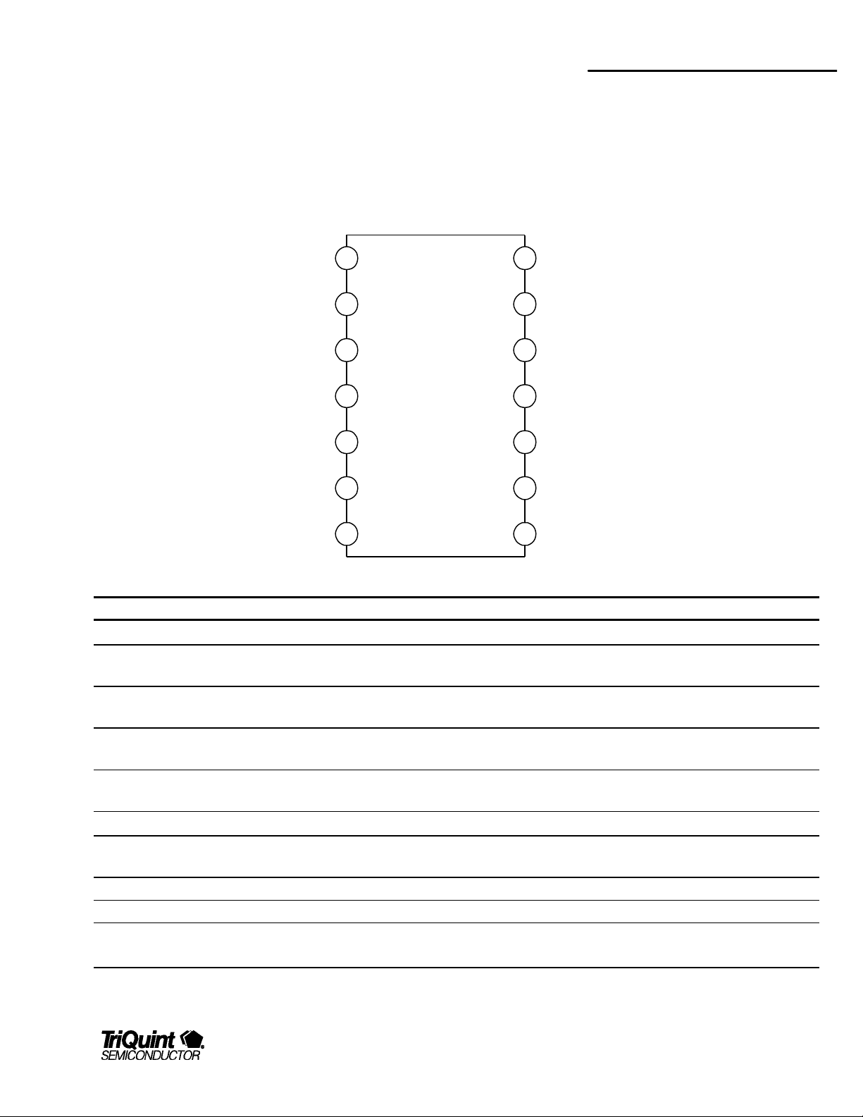
Package Pinout
TQ9203
Data Sheet
Mixer LO input
GND
Vdd
LNA IN0
Select
LNA IN1
GND GND
1
2
3
4
TQ9203
5
6
7
14
Mixer IF Output
13
LO Tune
12
GND
11
Mixer RF Input
10
GND
9
LNA Output
8
Pin Descriptions
Pin Name Pin # Description and Usage
Mixer LO IN 1
Vdd 3 Supply voltage for bias circuitry and LNA. This pin draws 8mA, typically. Decouple with 0.01uF within 0.25 inch of
LNA IN0 4 LNA IN0 is an auxiliary input and has characteristics similar to the LNA IN1 input port. Best performance is achieved
Select 5 Input port selection switch. CMOS-compatible drive, switches input ports from LNA IN1 to LNA IN0. Low=IN0,
LNA IN1 6 LNA IN1 is the primary input port. Best performance is achieved with external noise-matching network. Internally DC
LNA Out 9
Mixer RF IN 11 Mixer RF Input port. Image stripping band pass filtering before Mixer section improves noise and spurious performance.
LO Tune 13 LO buffer tuning, inductor to ground.
Mixer IF Out 14 Mixer IF signal port. Open “collector-” type output requires connection to Vdd and impedance matching to load.
GND 2,7,8,
10,12
Buffered LO port. There is an internal DC block on this port, which is matched to 50Ω.
package.
with external noise-matching network. Internally DC blocked.
High=IN1.
blocked.
Output port from switched LNA section. Internally matched to 50Ω. Internally DC blocked.
No return to ground is required. Shunt L recommended for IF suppression.
Ground connection. Keep physically short for stability and performance. Use several via holes immediately adjacent to
the pins down to backside ground plane.
For additional information and latest specifications, see our website: www.triquint.com 11
Page 12

TQ9203
Data Sheet
Package Type: SO-14 Plastic Package
Additional Information
For latest specifications, additional product information, worldwide sales and distribution locations, and information about TriQuint:
Web: www.triquint.com Tel: (503) 615-9000
Email: info_wireless@tqs.com Fax: (503) 615-8900
For technical questions and additional information on specific applications:
Email: info_wireless@tqs.com
The information provided herein is believed to be reliable; TriQuint assumes no liability for inaccuracies or omissions. TriQuint assumes no responsibility for the use of
this information, and all such information shall be entirely at the user's own risk. Prices and specifications are subject to change without notice. No patent rights or
licenses to any of the circuits described herein are implied or granted to any third party.
TriQuint does not authorize or warrant any TriQuint product for use in life-support devices and/or systems.
Copyright © 1998 TriQuint Semiconductor, Inc. All rights reserved.
Revision F, March 23, 1999
12 For additional information and latest specifications, see our website: www.triquint.com
 Loading...