

Page 1
WIRELESS COMMUNICATIONS DIVISION
TQ9147B
RF
GND
GND
GND
GND
RF
GND
V
OUT
1 16
2
3
4
5
6
IN
7
G1
RF
OUT
15
GND
14
GND
13
GND
GND
12
11
V
G2
10
GND
98
V
D1
Product Description
The TQ9147 is a high efficiency two stage GaAs MESFET power amplifier IC
intended for use in AMPS (IS-19) applications that operate in the US Cellular (824 849 MHz) band. The TQ9147 requires minimal external RF circuitry and operates
from a 4.8-Volt supply. With its flexible, off-chip, single component output matching
circuit, the TQ9147 is suitable for use in other applications near the cellular band,
such as 900 MHz ISM applications.
The TQ9147 utilizes a space saving SO-16 plastic package that minimizes board
area and cost.
DATA SHEET
2-Stage AMPS
Power Amplifier IC
Features
§ High Efficiency
§ +32 dBm Output Power
§ 50Ω Matched Input
§ SO-16 Plastic Package
§ Monolithic Power Amp
Applications
§ AMPS Mobile Phones
§ CDPD Modems
§ General ISM Band Applications
Electrical Specifications
Parameter Min Typ Max Units
Output Power +31.5 +32 dBm
Efficiency 55 60 %
Note 1: Test Conditions: VDD = 4.8 V, PIN = +7 dBm, Freq. = 824 & 849 MHz, TC = 25° C,
Min/max values 100% production tested.
1
Electrical Characteristics
For additional information and latest specifications, see our website: www.triquint.com 1
Page 2

TQ9147B
Data Sheet
Electrical Characteristics
Parameter
Frequency tuned for cellular band 824 849 MHz
Supply Voltage (VDD)
Temperature measured at case -40 25 +110
P
OUT
Efficiency 55 60 %
Rx band Noise
Small Signal Gain PIN = -10 dBm 32 dB
Power Gain P
Input Return Loss PIN = -30 to +7 dBm 10 dB
Harmonics
4th Harmonic
Spurious (Stability) PIN = -30 to +7 dBm -70 dBc/30 kHz
RF Off Isolation 20 dBc
Ruggedness VDD at burnout 6.5 V
Note 1: Test Conditions: VDD = 4.8 V, PIN = +7 dBm, Freq. = 824 & 849 MHz, VGG = 3.5 V, TC = 25° C.
Note 2: Noise power is measured in 30 kHz band width at the transmit frequency plus 45 MHz
Note 3: Load is set to 50 ohms, output power measured at nominal test conditions. Load VSWR is set to 10:1 and the angle is varied 360 degrees over 5 seconds.
1
Conditions Min Typ/Nom Max Units
2.7 4.8 6.0 V
2
2nd Harmonic
3rd Harmonic
VDD = 4.8 V
VDD = 4.3 V
PIN = -30 to +7 dBm -90 dBm
= 32 dBm (typ) 25 dB
OUT
31.5 32
30
-30
-35
-35
Load set to 50 ohms, output power remeasured and compared with the first measurement to check for no degradation from the first measurement.
o
C
dBm
dBm
dBc
dBc
dBc
Absolute Maximum Ratings
Parameter Value Units
DC Power Supply
1
8.0 V
DC Gate Voltage -5.0 V
RF Input Power 20 dBm
Storage Temperature -55 to 150
Operating Temperature (case) -40 to 110
Note 1: Into a 10:1 mismatch.
° C
° C
2 For additional information and latest specifications, see our website: www.triquint.com
Page 3
TQ9147B
Data Sheet
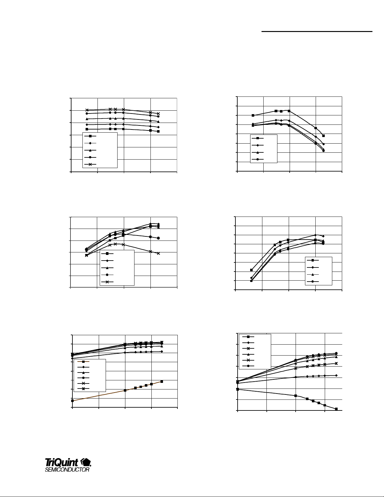
Typical Performance
Test Conditions (Unless Otherwise Specified): VDD = 4.8 V, PIN = +7 dBm, Freq. = 824 & 849 MHz, TC = 25° C, constant gate
voltages: VG1 = -1.5 V, VG2 = -2.2 V.
Output Power vs. Frequency and VDD
40
35
30
25
POUT (dBm)
20
15
VDD=3.0 V
VDD=3.6 V
VDD=4.6 V
VDD=5.8 V
VDD=7.0 V
10
750 800 850 900 950
Frequency (MHz)
Efficiency vs. Frequency and VDD
70
65
60
55
50
Efficiency (%)
45
VDD=3.0 V
VDD=3.6 V
VDD=4.6 V
VDD=5.8 V
VDD=7.0 V
40
750 800 850 900 950
Frequency (MHz)
Output Power vs. Frequency vs. Temp.
33.0
32.5
32.0
31.5
31.0
30.5
Pout (dBm)
30.0
29.5
-30 C
25 C
85 C
110 C
29.0
750 800 850 900 950
Frequency (MHz)
Efficiency vs. Frequency vs. Temp
70
68
66
64
62
60
Efficiency ( % )
58
56
-30 C
25 C
85 C
110 C
54
750 800 850 900 950
Freq ( MHz )
Output Power vs. Input Power vs. VD1
40
30
20
10
0
-10
POUT (dBm)
-20
Vd1=0V
Vd1=1V
Vd1=2V
Vd1=3V
Vd1=4V
Vd1=5V
-30
-40
-10 -5 0 5 10
PIN (dBm)
For additional information and latest specifications, see our website: www.triquint.com 3
Efficiency vs. Input Power vs. Vd1
100
80
60
40
Vd1=0V
Vd1=1V
Vd1=2V
Vd1=3V
Vd1=4V
Vd1=5V
20
Efficiency (%)
0
-20
-40
-10 -5 0 5
PIN (dBm)
Page 4

TQ9147B
Data Sheet
Harmonics vs. Frequency @ T = 25 C
-20
-30
-40
-50
Level (dBc)
-60
-70
-80
750 800 850 900 950
Frequency (MHz)
2nd Harm.
3rd Harm.
4th Harm.
-5
-7
-9
-11
-13
-15
S11 (dB)
-17
-19
-21
-23
-25
750 800 850 900 950
S11 vs. Frequency
Frequency (MHz)
Test Conditions (Unless Otherwise Specified): VDD = 5 V, PIN = +7 dBm, VGG = -3.5 V, Freq. = 824 & 849 MHz, TC = 25° C, Gate
voltage determined by the recommended bias circuit
Output Power vs. Frequency vs. VDD
33.2
33.0
32.8
32.6
(dBm)
32.4
OUT
P
32.2
32.0
31.8
820 825 830 835 840 845 850 855
Frequency (MHz)
VDD=4.75V
VDD=5V
VDD=5.25V
60.0
59.5
59.0
58.5
58.0
57.5
Efficiency (%)
57.0
56.5
56.0
820 825 830 835 840 845 850 855
Efficiency vs. Frequency vs. VDD
Eff, 4.75V
Eff, 5V
Eff, 5.25V
Frequency (MHz)
Output Power vs. Frequency vs. Temperature
33.0
32.9
32.8
32.7
32.6
32.5
32.4
Pout (dBm)
32.3
32.2
32.1
32.0
820 825 830 835 840 845 850 855
Frequency (MHz)
-30 C
25 C
110 C
60
59
58
57
56
55
Efficiency (%)
54
53
52
820 825 830 835 840 845 850 855
.
4 For additional information and latest specifications, see our website: www.triquint.com
Efficiency vs. Frequency vs. Temperature
-30 C
25 C
110 C
Frequency (MHz)
Page 5

TQ9147B
Data Sheet
Test Conditions (Unless Otherwise Specified): VDD = 5 V, PIN = +7 dBm, VGG = -3.5 V, Freq. = 824 & 849 MHz, TC = 25° C, Gate
voltage determined by the recommended bias circuit
Output Power vs. Frequency vs. Input Power
33.0
32.5
32.0
31.5
(dBm)
OUT
P
31.0
30.5
30.0
820 825 830 835 840 845 850 855
Frequency (MHz)
Pin=7dBm
Pin=3dBm
Pin=-2dBm
Efficiency vs. Frequency vs. Input Power
65
60
55
50
45
Efficiency (%)
40
35
30
820 825 830 835 840 845 850 855
Frequency (MHz)
Pin=7 dBm
Pin=3 dBm
Pin=-2 dBm
For additional information and latest specifications, see our website: www.triquint.com 5
Page 6

TQ9147B
Data Sheet
Application/Test Circuit
50 Ω Transmission Line
50 Ω Transmission Line
L1
1
RF
OUT
2
GND
3
GND
4
GND
RF
GND
V
TQ9147B
IN
G1
5
6
7
8
RF
GND
GND
GND
GND
16
OUT
15
14
13
12
11
V
G2
10
V
D1
C1
R1
C4
9
VD2 = 4.8 V
C2
R2
Q1
R5
C3
VD1 = 4.8 V
Q2
R3
R4
C5
VGG = -3.5 V
Bill of Material for TQ9147B Power Amplifier Application/Test Circuit
Component Reference Designator Part Number Value Size Manufacturer
Power Amplifier IC U1 TQ9147B TSSOP-20 TriQuint Semiconductor
PNP Transistor Q1, Q2 2N3906
Capacitor C1, C4, C5 MCH182F104ZK
0.1 µF
Capacitor C2, MCH155A8R2CK 8.2 pF 0402 Rohm
Capacitor C3 MCH155A680JK 68 pF 0402 Rohm
Resistor R1 MCR01JW510
Resistor R2 MCR01JW100
Resistor R3 MCR01JW621
Resistor R4 MCR01JW202
Resistor R5 MCR01JW391
51 Ω
10 Ω
620 Ω
2 kΩ
390 Ω
Inductor L1 0805CS470 47 nH Coilcraft
0603 Rohm
0402 Rohm
0402 Rohm
0402 Rohm
0402 Rohm
0402 Rohm
6 For additional information and latest specifications, see our website: www.triquint.com
Page 7

TQ9147B
Data Sheet
Product Description
The TQ9147 is a high efficiency two stage GaAs MESFET
power amplifier IC intended for use in AMPS (IS-19)
applications that operate in the US Cellular (824 - 849 MHz)
band. The TQ9147 requires minimal external RF circuitry and
operates from a 4.8-Volt supply. With its flexible, off-chip, single
component output matching circuit, the TQ9147 is suitable for
use in other applications near the cellular band, such as 900
MHz ISM applications.
The TQ9147 utilizes a space saving SO-16 plastic package that
minimizes board area and cost.
Operation
Please refer to the application circuit above.
Gate Biasing and Bypassing
The TQ9147 is a dual-supply power amplifier (PA). Because it
utilizes depletion-mode MESFETs, a negative bias voltage must
be supplied to the gate of each FET. There are several
excellent choices of negative voltage bias supplies (charge
pumps) on the market, such as the Maxim MAX881R, or the
Harris ILC7660S. A simple resistor divider circuit is the most
inexpensive way to bias the gates of each stage from the charge
pump. However, due to fabrication tolerances and the large
window of main supply voltages under which the device can
function, the active bias method shown in the application circuit
is recommended.
This bias technique accurately sets the bias point for each stage
and optimizes the quiescent current and efficiency over a wide
range of supply voltages and output power levels. The following
table lists the nominal values of gate voltage and quiescent
current when this bias method is used. It is important to
remember that the negative gate voltage must be supplied first
in order to protect the device from inadvertent high drain
currents. If the drains are turned on before the gate bias is set,
the IC can be damaged or destroyed.
Gate Bias Voltages and Drain Quiescent Current
Parameter Value Units
V
DD
V
G1
V
G2
I
DQ1
I
DQ2
4.8 V
-1.5 V
-2.2 V
50 MA
0-100 mA
The gate of each FET in the IC is RF bypassed on chip.
However, additional low frequency filtering and noise
suppression must be done externally. This is accomplished with
a 51 Ohm resistor (R1) and 0.1 µF cap (C4) from pin 11 (Vg2).
This capacitor and resistor combination also ensures device
stability under all conditions.
Drain Bypassing
C1 (0.1 µF) provides RF bypassing for the high impedance side
of the RF choke (L1).
Input Match
The device input is internally matched to 50 Ohms. A 50-Ohm
transmission line is all that is required between the PA and the
driver amp.
Output Match and High Power Bias Injection
Pins 1 and 16 are dual-purpose pins, providing for both the RF
output and the high power DC input for the drain of the second
stage FET. As such, these pins are connected to a 50-Ohm
transmission line. Locating C2 (8.2 pF) approximately 200 mils
from the device along this transmission line acts as a shorted
stub tuner that transforms the low output impedance (~ 7.5
Ohms) of the power stage to 50 Ohms. Varying the position of
C2 along the line can alter the output match in order to optimize
either power output or efficiency. In general, the farther away
C2 is from the pins the higher the efficiency at the expense of
power output. The closer the cap is, the higher the output
power at the expense of efficiency. By varying the value and
position of C2, the device can be easily tuned for a different
frequency range such as the 902 – 928 MHz ISM band. C3 (68
pF) is a DC blocking cap.
For additional information and latest specifications, see our website: www.triquint.com 7
Page 8

TQ9147B
Data Sheet
Drain current for the second stage is injected through L1 (47
nH), which acts as an RF choke on the high power DC feed line.
As stated above, C1 is the bypass cap for the high impedance
side of L1.
Power down Function
To fully turn off the PA when not transmitting, a PMOS FET
(PFET) switch can be used to control the drain bias to the PA.
There are several acceptable models available on the market,
such as the IRF7604 from International Rectifier, or any device
with low R
this type is that it protects the PA from inadvertently powering up
the device incorrectly. Since depletion-mode FETs are used in
the PA, care must be taken to insure that the gate bias is fully
stabilized before drain bias is applied. If not, the full value of I
will flow, which could damage or destroy the IC. A feature
included in the Maxim charge pump allows for a separate
control output to run the PFET. This control line holds the PFET
off until the gate bias voltage has stabilized.
. An added benefit of incorporating a switch of
DSon
Dss
RF Power Control
There are three methods of controlling the output power from
the TQ9147. All three methods can provide a minimum 25 dB of
control range for the device, which exceeds the requirements of
IS-19.
The first method is to vary the gate bias voltages. Though this
approach has the advantage of increased efficiency at lower
output power levels, it is hampered by two problems. First, both
gate voltages must be varied. Since each stage typically
requires a different bias point, the control circuit must monitor
both bias points, thereby complicating the design.
The second drawback is that most charge pumps, including
those recommended above, require large capacitors on the
output for filtering and stability. Such large cap values may not
allow full compliance with the required 20 mS transition spec
between any two power levels.
The second method is to vary the input power level. Though
this can be done with a simple attenuator between the driver
amp and the PA, the response is very non-linear, as the PA
must first come out of saturation before the output power can
change. Once out of saturation, the first stage is class A biased,
which means that the drain current is constant regardless of
power settings. The addition of an attenuator also adds to the
expense of the parts list and to the board size equation, and
increases the insertion loss the driver amp must overcome.
The third, and preferred, method is to vary the drain supply
voltage to the first stage. By forcing the first stage bias lower,
the first stage is always heavily saturated, thus saving battery
power. Since the second stage is biased class AB, drain current
to that stage lowers as the drive level decreases. This method
optimizes battery savings over the other approaches. The
simplest implementation of this technique would be to
incorporate a second PFET to control the first stage drain. This
circuit can be realized buy utilizing a dual PFET such as the
International Rectifier IRF7314, which has two low R
a single SO-8 package. By cascoding the two FETs, one
implements a master on/off function while the second controls
only the first stage drain bias. This technique also fits very well
with the active gate biasing circuit that was recommended
previously.
DSon
FETs in
8 For additional information and latest specifications, see our website: www.triquint.com
Page 9

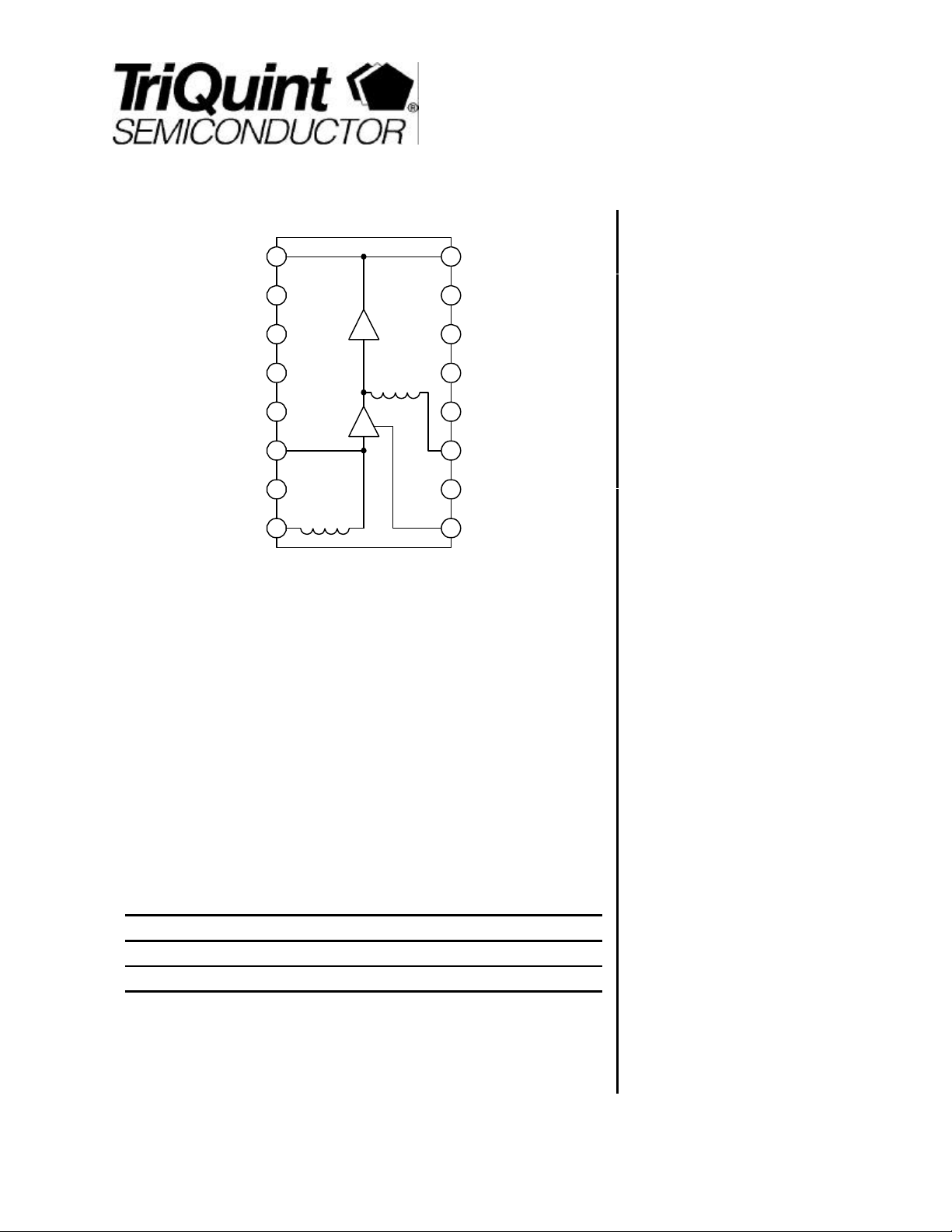
Package Pinout
TQ9147B
Data Sheet
RF
OUT
GND
V
G3
GND
RF
IN
GND
V
G1
Pin Descriptions
Pin Name Pin # Description and Usage
RF
OUT
RF
IN
V
G1
V
D1
V
G2
GND 2, 3, 4, 5, 7,
1,16 Power Amplifier output and second-stage supply voltage. Critical, but simple, matching circuit required. Bias choke for V
required, local bypass cap recommend, and DC blocking capacitor required.
6
RF input to power amplifier. Matched to 50 Ω. Internal DC block.
8 First stage gate voltage. Local bypass cap needed. Set VG1 = -1.5 V or use bias stabilization circuit.
9 First stage supply voltage. Local bypass cap recommended. Use same voltage as VD2 or use bias stabilization circuit.
11
Second stage gate voltage. Local bypass cap needed. Required 50 Ω series resistor near device for stability. Set
VG2 = -2.2 V or use bias stabilization circuit.
Ground connections. Provide thermal path for heat dissipation and RF grounding. Very important to place multiple via holes
10, 12, 13,
immediately adjacent to the pins.
14, 15
1
2
3
4
5
6
7
8
TQ9147B
16
RF
OUT
15
GND
14
V
D2
13
GND
12
11
V
G2
10
GND
9
V
D1
D2
Revision AA June 30November, 1998
TQS Wireless Communications • 2300 NE Brookwood Parkway • Hillsboro, OR 97124 • (503) 615-9000 • FAX:(503) 6158900
Page 10
TQ9147B
Data Sheet
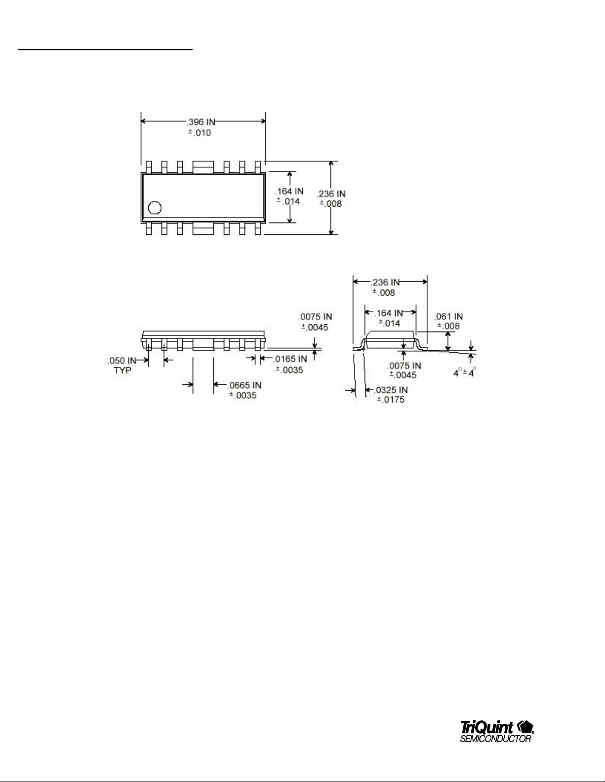
Package Type: SOIC-16 Plastic Package with Thermal Tabs
Additional Information
For latest specifications, additional product information, worldwide sales and distribution locations, and information about TriQuint:
Web: www.triquint.com Tel: (503) 615-9000
Email: info_wireless@tqs.com Fax: (503) 615-8900
For technical questions and additional information on specific applications:
Email: info_wireless@tqs.com
The information provided herein is believed to be reliable; TriQuint assumes no liability for inaccuracies or omissions. TriQuint assumes no responsibility for the use of
this information, and all such information shall be entirely at the user's own risk. Prices and specifications are subject to change without notice. No patent rights or
licenses to any of the circuits described herein are implied or granted to any third party.
TriQuint does not authorize or warrant any TriQuint product for use in life-support devices and/or systems.
Copyright © 1998 TriQuint Semiconductor, Inc. All rights reserved.
Revision B, March 18, 1999
10 For additional information and latest specifications, see our website: www.triquint.com
 Loading...