

Page 1
WIRELESS COMMUNICATIONS DIVISION
TQ9132B
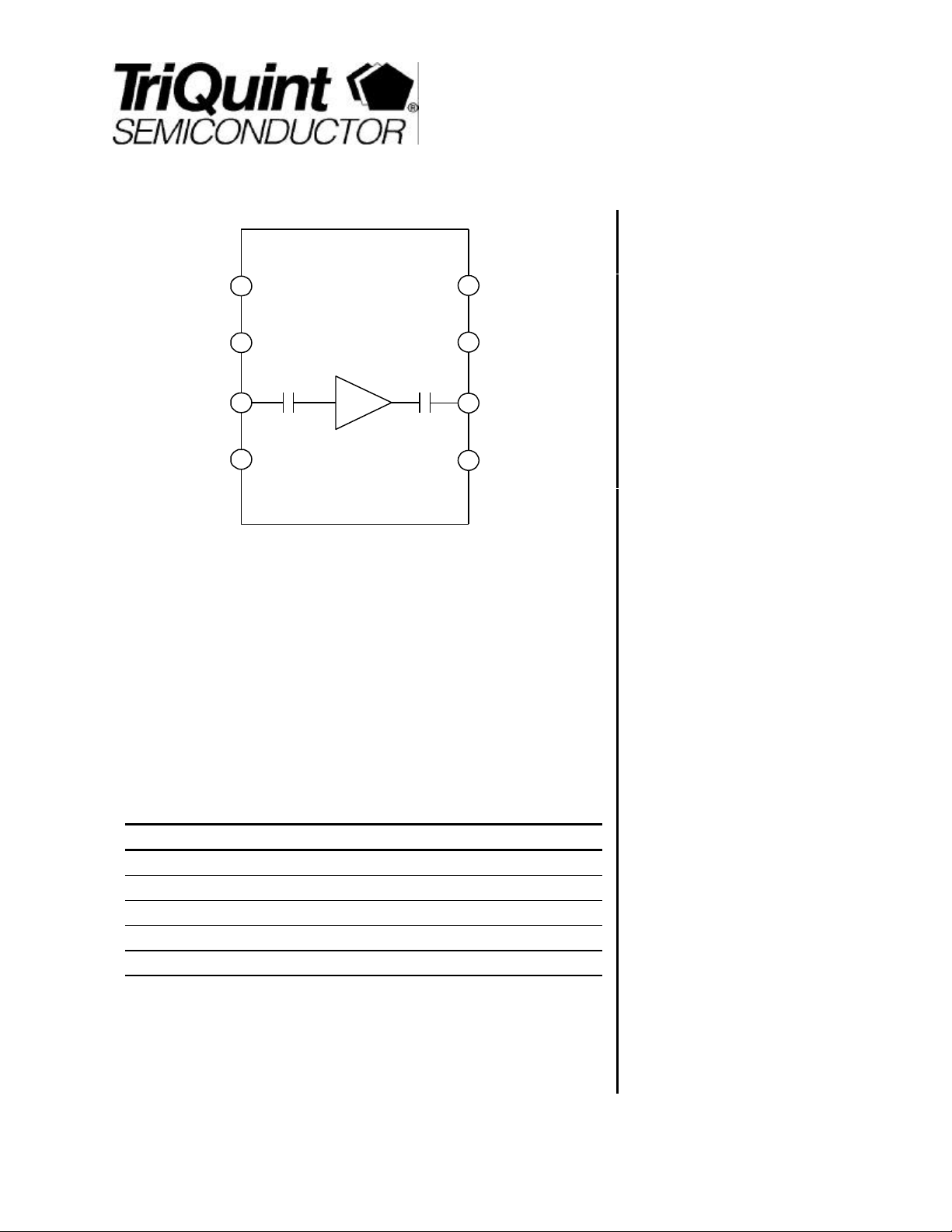
VDD
1
DATA SHEET
GND
8
GND
GND GND
IN
2
3
4
GND
7
6
OUT
5
TQ9132B
Product Description
The TQ9132B amplifier is an 800-2500 MHz amplifier capable of providing moderate
output power (50 mW) for a wide variety of transmit and receive applications. The
amplifier’s input and output are matched to 50 Ω with internal circuitry, simplifying
interfaces to 50 Ω systems. In addition, DC blocking capacitors are included on chip,
permitting direct connections to the input and output. Its 8-pin surface mount
package and low cost are well suited to many wireless communications applications.
Electrical Specifications
1
3V Cellular TDMA/AMPS
Power Amplifier IC
Features
§ Single 3V- 6V supply
§ Wide frequency range
§ +17 dBm output power
§ Input and output matched to 50 Ω
§ SO-8 surface mount plastic package
Applications
§ Power Amplifier drivers
§ PCN Medium-power amplifiers
§ Medium-power WLANs
Parameter Min Typ Max Units
Gain 13.5 16 dB
Output 1 dB Gain Compression 15.5 17 dBm
Input Return Loss 12 dB
Output Return Loss 12 dB
DC Supply Current 85 100 MA
Note 1: Test Conditions: VDD = 5.0 V, Freq. = 2500 MHz, TA= 25° C.
Note 2: . Min/max values 100% production tested
Electrical Characteristics
For additional information and latest specifications, see our website: www.triquint.com 1
§ CDPD Modems
§ Base Station receivers
Page 2
TQ9132B
Data Sheet
Electrical Characteristics
Parameter Conditions Min. Typ/Nom Max. Units
Frequency 800 800 to 2500 2500 MHz
Supply Voltage (VDD)
Gain 13.5 16 dB
Noise Figure 4.1 dB
Output 1 dB Gain Compression 15.5 17 dBm
Output 3rd Order Intercept 27 dBm
Input Return Loss 12
Output Return Loss 12 10 dB
DC Supply Current 85 100 mA
Note 1: Test Conditions: VDD = 5.0 V, Freq. = 2500 MHz, TA= 25° C.
Note 2: . Min/max values 100% production tested
Absolute Maximum Ratings
3.0 5.0 6.0 V
10
dB
Parameter Value Units
DC Power Supply 7.0 V
Power Dissipation 500 mW
Input Power +10 dBm
Storage Temperature -55 to 150
Operating Temperature (case) -40 to 70
Thermal Resistance 135.5
° C
° C
o
C/W
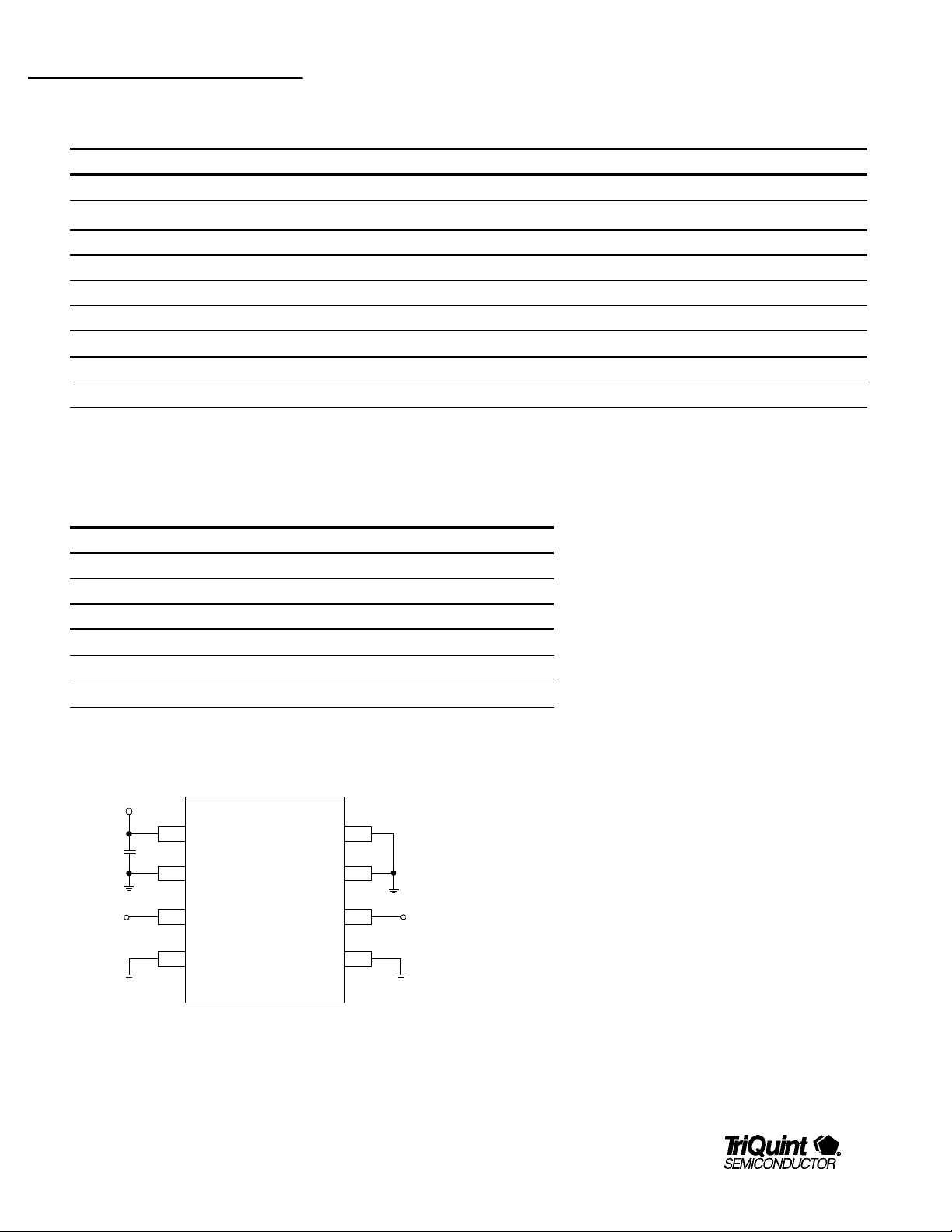
Application/Test Circuit
VDD
0.01 µF
Input
1
2
GND
TQ9132B
3
IN
GND GND
4
GND
GND
OUT
8VDD
7
6
5
Output
2 For additional information and latest specifications, see our website: www.triquint.com
Page 3
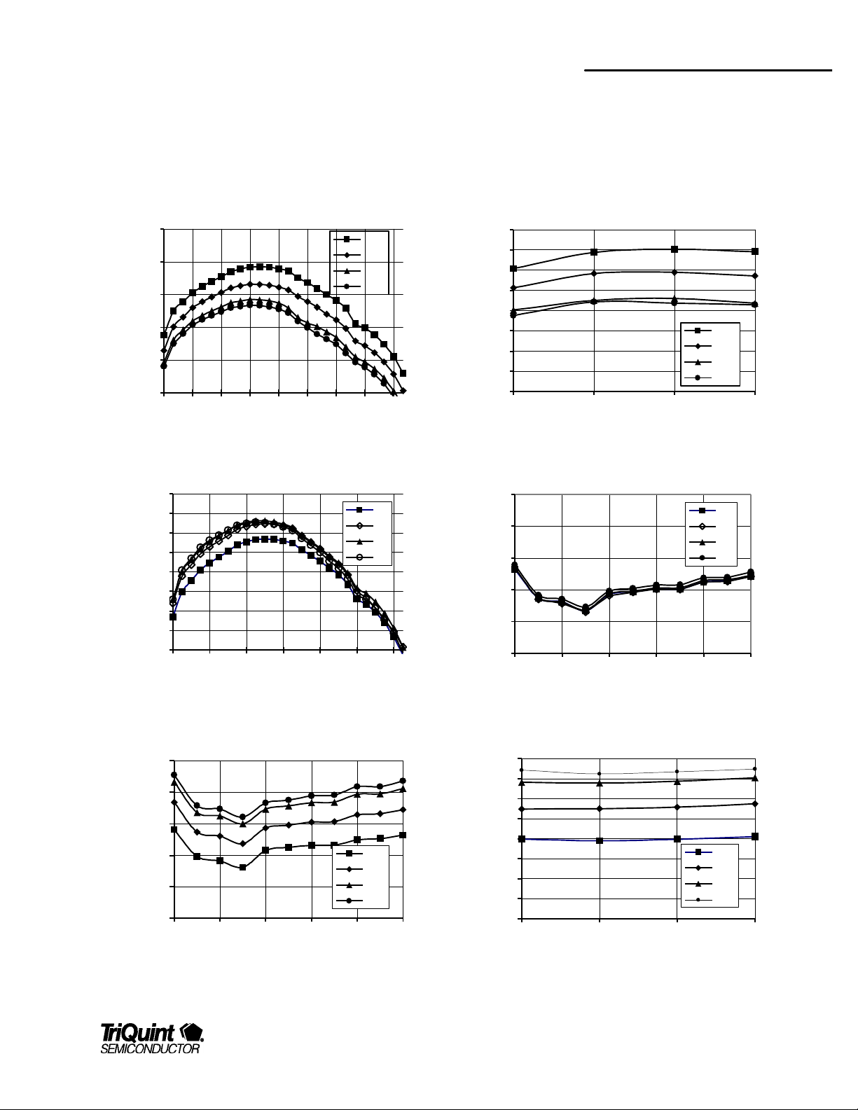
Typical Performance
Gain vs. Frequency vs. Vdd
Test Conditions (Unless Otherwise Specified): VDD = 5 V, Freq. = 2500 MHz, TC = 25° C.
TQ9132B
Data Sheet
Gain vs. Frequency vs. Temperature (Vdd = 5V)
22
20
18
16
Gain (dB)
14
12
500 800 1100 1400 1700 2000 2300 2600 2900
Frequency (MHz)
20
19
18
17
16
Gain (dB)
15
14
13
12
500 900 1300 1700 2100 2500 2900
Frequency (MHz)
-40 C
25 C
70 C
85 C
3 V
4V
5V
6V
Gain vs. Vdd vs. Temperature (1900 MHz)
20
19
18
17
16
Gain (dB)
15
14
13
12
3.0 4.0 5.0 6.0
Vdd (V)
NF vs. Frequency vs. Vdd
8.0
7.0
6.0
NF (dB)
5.0
4.0
3.0
500 1000 1500 2000 2500 3000
Frequency (MHz)
-40 C
25 C
70 C
85 C
3 V
4 V
5 V
6 V
NF vs. Frequency vs. Temperature
7.0
6.0
5.0
4.0
NF (dB)
3.0
2.0
500 1000 1500 2000 2500 3000
Frequency (MHz)
For additional information and latest specifications, see our website: www.triquint.com 3
-40 C
25 C
70 C
85 C
NF vs. VDD vs. Temperature
6.5
6.0
5.5
5.0
4.5
NF (dB)
4.0
3.5
3.0
2.5
3.0 4.0 5.0 6.0
VDD (V)
-40 C
25 C
70 C
85 C
Page 4

TQ9132B
Data Sheet
Typical Performance
Test Conditions (Unless Otherwise Specified): VDD = 5 V, Freq. = 2500 MHz, TC = 25° C.
P1dB vs. Frequency vs. Temperature (Vdd = 3V)
19
17
15
13
P1dB (dBm)
11
9
500 1000 1500 2000 2500 3000
Freq (MHz)
P1dB vs. Frequency vs. Vdd
23
21
19
17
15
P1dB (dBm)
13
11
9
500 1000 1500 2000 2500 3000
Frequency (MHz)
-40 C
25 C
70 C
85 C
3 V
4 V
5 V
6 V
P1dB vs. VDD vs. Temperature
18
16
14
P1dB (dBm)
12
3.0 4.0 5.0 6.0
VDD (V)
IP3 vs. Frequency vs. VDD
34
32
30
3 V
4 V
5 V
6 V
28
IP3 (dBm)
26
24
22
500 1000 1500 2000 2500 3000
Frequency (MHz)
-40 C
25 C
70 C
85 C
IP3 vs. Frequency v.s Temperature
32
31
30
29
IP3 (dBm)
28
27
26
500 1000 1500 2000 2500 3000
Frequency (MHz)
-40 C
25 C
70 C
85 C
28
27
26
IP3 (dBm)
25
24
3.0 4.0 5.0 6.0
4 For additional information and latest specifications, see our website: www.triquint.com
IP3 vs. VDD vs. Temperature
-40 C
25 C
70 C
85 C
VDD (V)
Page 5

Typical Performance
Test Conditions (Unless Otherwise Specified): VDD = 5 V, Freq. = 2500 MHz, TC = 25° C.
TQ9132B
Data Sheet
S11 vs. Frequency vs. VDD
0
-5
-10
-15
S11 (dB)
-20
-25
-30
500 1000 1500 2000 2500 3000
Frequency (MHz)
S22 vs. Frequency vs. VDD
-10
-15
-20
-25
S22 (dB)
-30
-35
3V
4V
5V
6V
500 1000 1500 2000 2500 3000
Frequency (MHz)
3 V
4 V
5 V
6 V
S12 vs. Frequency vs. VDD
-25
-30
-35
-40
-45
S12 (dB)
-50
-55
-60
500 1000 1500 2000 2500 3000
Frequency (MHz)
3V
4V
5V
6V
For additional information and latest specifications, see our website: www.triquint.com 5
Page 6

TQ9132B
Data Sheet
S-Parameters (typical)
Freq (MHz) | S11 |
500 0.769 -110 5.2 22 0.012 83 0.157 12
600 0.644 -127 5.9 -15 0.010 17 0.159 -44
700 0.543 -144 6.5 -48 0.011 -17 0.185 -77
800 0.450 -159 7.0 -78 0.010 -38 0.206 -103
900 0.382 -172 7.4 -106 0.010 -56 0.216 -126
1000 0.326 92 7.7 -132 0.010 -72 0.219 -150
1100 0.281 166 7.9 -158 0.010 -85 0.221 -125
1200 0.247 157 8.2 152 0.010 -98 0.214 -164
1300 0.220 147 8.4 151 0.010 -109 0.204 140
1400 0.199 137 8.5 126 0.009 -120 0.194 118
1500 0.177 126 8.6 102 0.009 -130 0.185 92
1600 0.154 113 8.6 78 0.009 -137 0.175 64
1700 0.131 99 8.5 53 0.009 -133 0.165 36
1800 0.102 85 8.4 30 0.010 -141 0.165 7
1900 0.072 62 8.1 6 0.011 -158 0.165 -24
2000 0.053 -2 7.8 -17 0.012 -155 0.171 -54
2100 0.050 -49 7.5 -39 0.013 -127 0.18 -82
2200 0.063 -105 7.2 -62 0.015 137 0.188 -107
2300 0.085 -84 6.7 -84 0.016 159 0.194 -128
2400 0.119 58 6.4 -105 0.017 147 0.199 -148
2500 0.153 149 6.0 -127 0.019 134 0.201 -107
2600 0.182 146 5.6 -147 0.020 120 0.199 -8
2700 0.210 131 5.3 -132 0.021 107 0.198 160
2800 0.234 117 5.0 135 0.023 93 0.196 145
2900 0.258 103 4.7 151 0.024 76 0.191 128
3000 0.285 86 4.4 131 0.025 63 0.178 112
1
∠S11
| S21 |
∠S21
| S12 |
∠S12
| S22 |
∠S22
Note 1: Test Conditions: VDD = 5.0 V, Freq. = 2500 MHz, TA= 25° C. Reference plane at package leads.
6 For additional information and latest specifications, see our website: www.triquint.com
Page 7

Package Pinout
TQ9132B
Data Sheet
GND
1
2
8VDD
GND
7
GND
TQ9132B
IN
3
4
GND GND
6
OUT
5
Pin Descriptions
Pin Name Pin # Description and Usage
V
DD
1
Voltage from desired power supply. Decoupling is required. Decouple with a 0.01 µF capacitor within 5 mm of package.
IN 3 RF Input. Internally DC blocked and matched to 50 ohms. Connect directly to any 50 ohm source with 50 ohm printed
microstrip line.
OUT 6 RF Output. Internally DC blocked and matched to 50 ohms. Connect directly to any 50 ohm source with 50 ohm printed
microstrip line.
GND 2,4,5,7,8 Ground connections. Connect immediately to ground plan for stability and performance. Pins are internally connected.
Simplified Schematic
1
19 nH
.
3 pF
300
Ω
1.3 nH 8
3
15 pF
2,5,7,8
Ω
.
35 pF
7.9 pF 3 nH
.2 pF
5K
35 pF
65
Ω
500
35 pF 5K
19 nH
.
3 pF
Ω
35 pF
6.5 pF
.1 pF
15
Ω
6
Revision AA June 30November, 1998
TQS Wireless Communications • 2300 NE Brookwood Parkway • Hillsboro, OR 97124 • (503) 615-9000 • FAX:(503) 6158900
Page 8

TQ9132B
_
_+_+_+_+_+_+_+_+_
_
Data Sheet
Package Type: SO-8 Plastic Package
.199 IN
+
.010
.050 IN
TYP
.164 IN
.014
.0075 IN
.0165 IN
.0035
.236 IN
+
.0045
.008
.236 IN
.008
.164 IN
.014
.0075 IN
.0045
.0325 IN
.0175
.061 IN
.008
4 4
O
O
+
Additional Information
For latest specifications, additional product information, worldwide sales and distribution locations, and information about TriQuint:
Web: www.triquint.com Tel: (503) 615-9000
Email: info_wireless@tqs.com Fax: (503) 615-8900
For technical questions and additional information on specific applications:
Email: info_wireless@tqs.com
The information provided herein is believed to be reliable; TriQuint assumes no liability for inaccuracies or omissions. TriQuint assumes no responsibility for the use of
this information, and all such information shall be entirely at the user's own risk. Prices and specifications are subject to change without notice. No patent rights or
licenses to any of the circuits described herein are implied or granted to any third party.
TriQuint does not authorize or warrant any TriQuint product for use in life-support devices and/or systems.
Copyright © 1998 TriQuint Semiconductor, Inc. All rights reserved.
Revision B, January 7, 1999
8 For additional information and latest specifications, see our website: www.triquint.com
 Loading...