

Page 1
T R I Q U I N T S E M I C O N D U C T O R , I N C .
1
PRELIMINARY DATA SHEET
For additional information and latest specifications, see our website: www.triquint.com
TELECOM
PRODUCTS
The TQ8105/TQ8106 are SONET/SDH transceivers that integrate
multiplexing, demultiplexing, SONET/SDH framing, clock-synthesis PLL, and
enhanced line and clock diagnostic functions into a single monolithic device.
The TQ8106 is a pin-compatible upgrade of the TQ8105 that includes a
Clock and Data Recovery (CDR) function. The TQ8105 and TQ8106 allow
maximum flexibility in the selection of internal/external Clock and Data
Recovery, Opto-Electronic (O/E) Module, and Reference Clock Sources.
On-chip PLLs use external RC-based loop filters to allow custom tailoring of
loop response and support the wide range of reference clock frequencies
found in SONET/SDH/ATM systems. For transmit clock synthesis or for CDR,
the PLLs exceed ANSI, Bellcore, and ITU jitter specifications for systems
when combined with industry-typical O/E devices such as Sumitomo, AT&T,
HP, and AMP. The TQ8105/TQ8106 PLLs provide byte clocks and constantrate 38.88 MHz and 51.84 MHz, synthesized clock outputs, providing
clocking for UTOPIA and other system busses. Transmit data may also be
clocked into the devices with respect to the reference clock.
Operating from a single +5V supply, the TQ8105/TQ8106 provides fully
compliant functionality and performance, utilizing direct-connected PECL
levels (differential or single-ended) for high-speed I/O. As compared to ACcoupled schemes, the direct-coupled connections reduce jitter and
switching-level offsets due to data patterns. The TQ8105/TQ8106 can also
provide direct connection to high-speed I/O utilizing ECL levels with a –5V
supply. Low-speed bus, control, and clock I/O utilize TTL levels. (An ECL/
PECL reference clock input is also provided; at 155.52 MHz the input should
be only PECL/ECL.) Output TTL pins can be tristated and may also be
configured for V
OH
with a 3.3V supply connection.
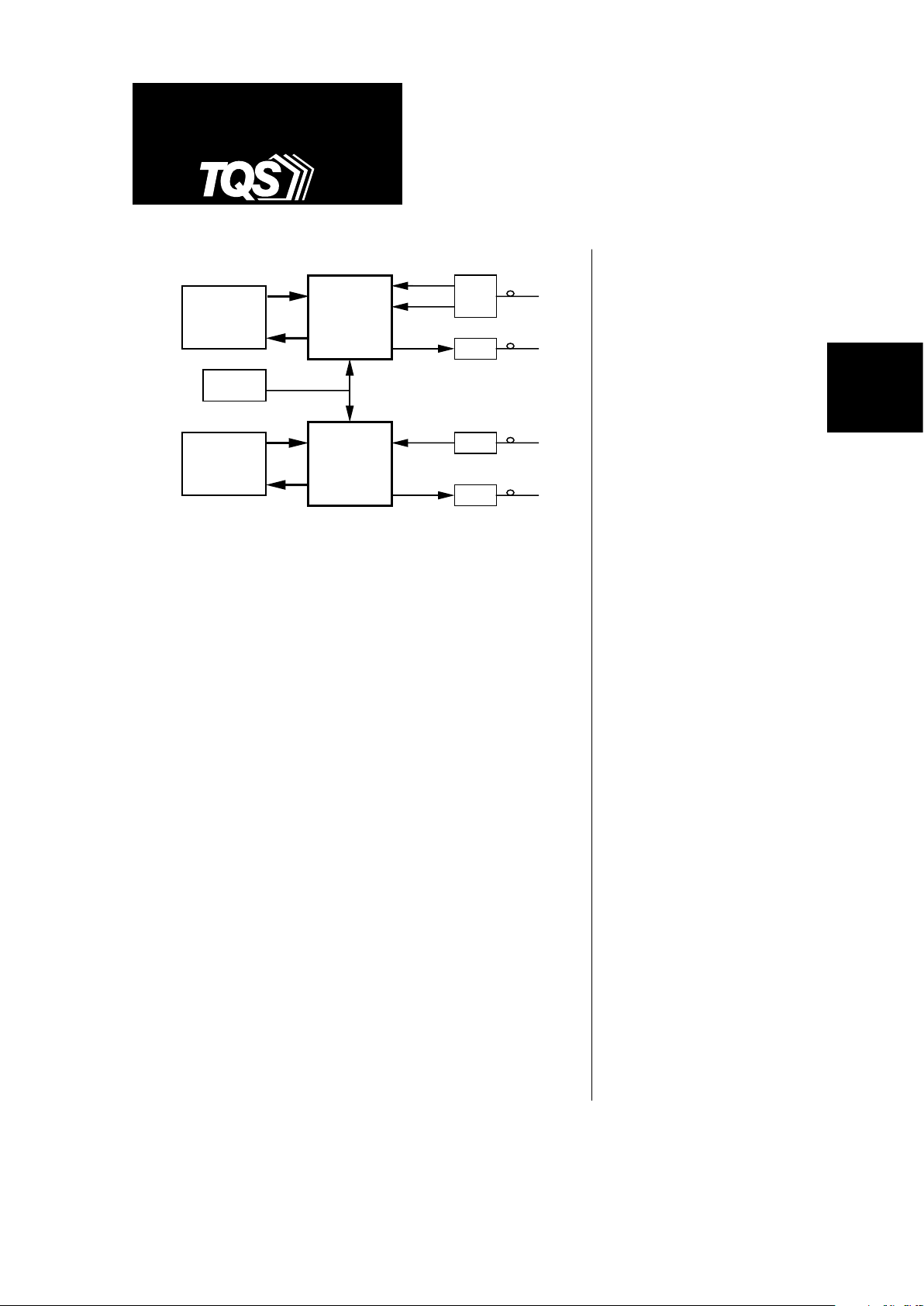
TQ8105/8106
SONET/SDH
Overhead
Processor
TQ8105
or
TQ8106
SONET/SDH
Transceiver
Tx O/E
Rx O/E
with
CDR
SONET/SDH
Overhead
Processor
TQ8106
SONET/SDH
Transceiver
with CDR
Tx O/E
Rx O/E
Reference
Clock
SONET/SDH
Transceivers
Features
• Single-chip, byte-wide Mux,
Demux, Framer, and Tx clocksynthesis PLL with enhanced
diagnostics
• TQ8106 includes monolithic
Clock and Data Recovery
• SONET/SDH/ATM compliant for
STS-12/STM-4 (622 Mb/s) or
STS-3/STM-1 (155 Mb/s) rates
• 155.52, 77.76, 51.84, 38.88, or
19.44 MHz reference clock inputs
with TTL, PECL, or ECL level
• 38.88 MHz and 51.84 MHz clock
outputs for UTOPIA as well as
byte clock rate (77.76 or 19.44 MHz)
• External RC-based loop filters
• Integrated loopbacks with
enhanced line and reference
clock diagnostics
• Direct-coupled standard, PECL,
high-speed I/O with ECL option
• Clean TTL interface to
PMC-Sierra devices
• 100-pin 14x14 mm JEDEC
plastic package
• +5V-only supply for PECL I/O
(–5.2V required for ECL I/O option)
• –40 to +125°C case operating
temperature
Page 2
2
TQ8105/TQ8106
PRELIMINARY DATA SHEET
For additional information and latest specifications, see our website: www.triquint.com
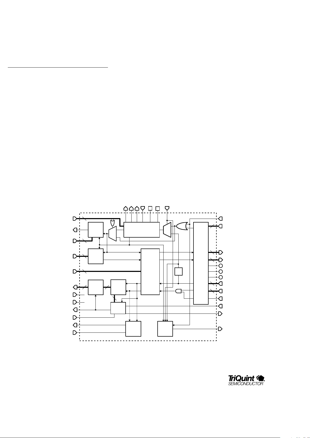
Figure 1. TQ8105 Block Diagram
The combination of a thermally enhanced, 100-pin
JEDEC, metric, plastic package, the low-power
dissipation of the device, and the wide casetemperature range permits operation without a heat
sink in most designs.
The TQ8106 uses the same pinout as the TQ8105 and
is compatible with it.
The TQ8105/TQ8106 provides comprehensive,
integrated, loopback functionality and enhanced line
and reference clock diagnostics required of SONET/
SDH systems, minimizing additional external circuitry.
TQ8105/TQ8106 diagnostics include:
• Loss of Reference clock detector (LOR) output to
indicate that the PLL Reference Clock is not toggling
• Lock Indicator (RLOCK), which permits monitoring
of the receiver clock frequency, flagging when the
frequency drifts beyond approximately 500 ppm
• Loss of Signal (LOS) detector output to indicate that
the incoming data stream has no data transitions in
128-bit periods
• ECL/PECL input (NSOL) to allow LOS from an O/E
module to force the data stream to all zeroes,
eliminating the need for external glue logic.
CKSRC(2:0)
MXD(7:0)
TXD
TXCK
RXD
RXCK
2
2
2
2
ECL/
PECL
I/O
Block
DVPP
8
Parallel
to
Serial
DXD(7:0)
8
LBM(1:0)
2
PH(1:0)
2
Loop
Back &
Retime
Block
LOS
Detect
VPP
VNN
FP1
REFCKE
2
REFCKT
B
Y
A
B
Y
A
MMS
Clock
Data
Clock
Data
Clock
Data
Clock
Data
/8
Ext. Clk
OC3
11
Hold
Register
NOE
LOS
DXSYNC
OOF
8
Serial
to
Parallel
Clock
Phase
TxBC
RxBC
Framer
Clock/8
LOR
NRESET
SDHCK
3
PLL Clock
Synthesizer
FP2
NSOL
SONETC
K
CLRLOS
Freq.
Lock
Detect
RLOCK
FRPWR
TQ8105
Page 3
TQ8105/TQ8106
3
PRODUCTS
PRELIMINARY DATA SHEET
For additional information and latest specifications, see our website: www.triquint.com
TELECOM
PRODUCTS
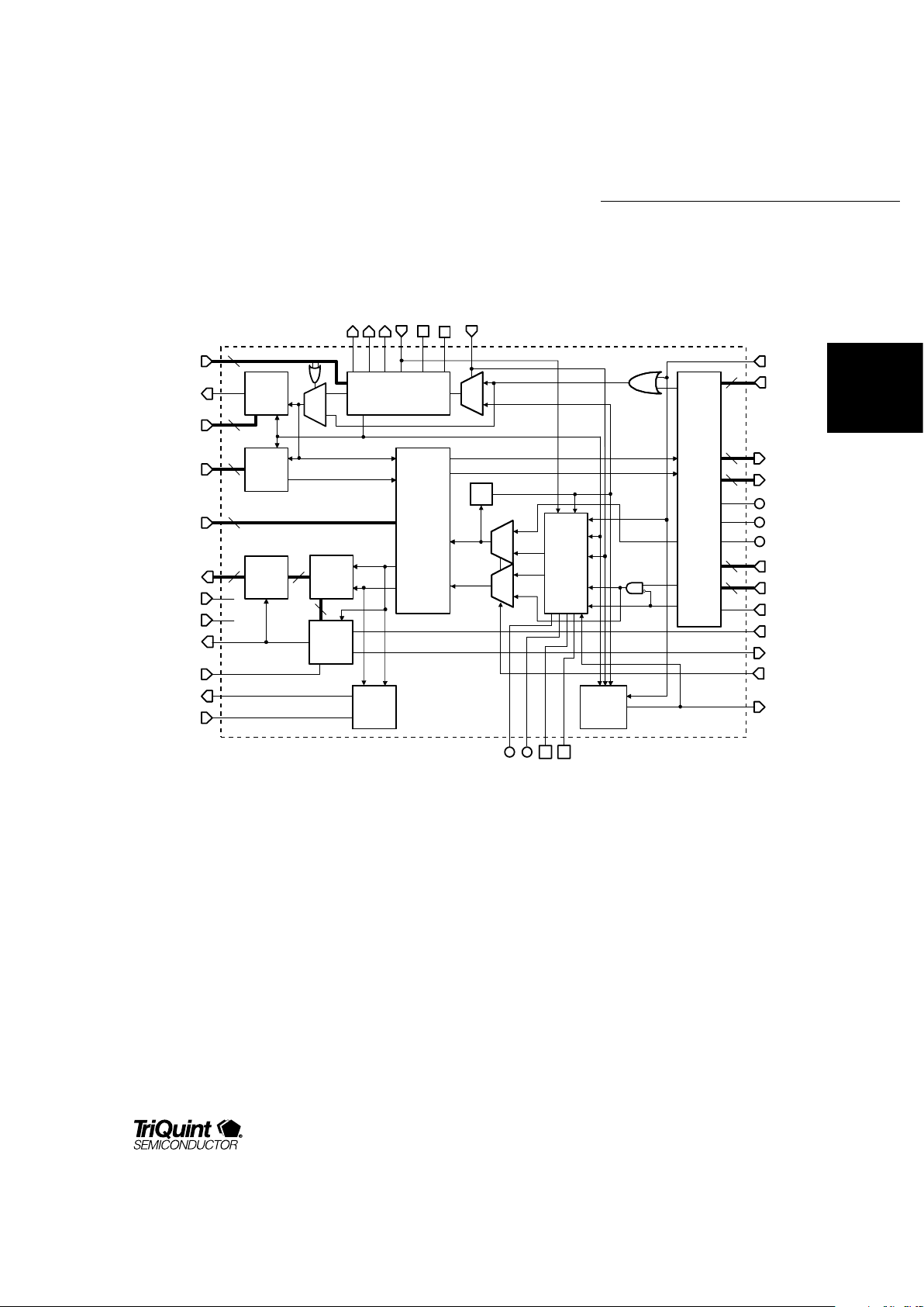
Figure 2. TQ8106 Block Diagram
CKSRC(2:0)
MXD(7:0)
TXD
TXCK
RXD
RXCK
2
2
2
2
ECL/
PECL
I/O
Block
DVPP
8
Parallel
To
Serial
DXD(7:0)
8
LBM(1:0)
2
PH(1:0)
2
Loopback
& Retime
Block
LOS
Detect
VPP
VNN
FP1
REFCKE
2
REFCKT
B
Y
A
MMS
Clock
Data
Clock
Data
Clock
Data
Clock
Data
/8
Ext. Clk
OC3
11
Hold
Register
NOE
LOS
DXSYNC
OOF
8
Serial
To
Parallel
Clock
Phase
TxBC
RxBC
Framer
Clock/8
LOR
NRESET
SDHCK
3
PLL Clock
Synthesizer
FP2
NSOL
SONETCK
CLRLOS
Freq.
Lock
Detect
RLOCK
FRPWR
B
Y
A
B
Y
A
B
Y
A
Clock
& Data
Recovery
Data
Clock
NCDREN
CDRFP2
CDRFP1
CDRGND
CDRAVDD
Clock
Data
TQ8106
Page 4
4
TQ8105/TQ8106
PRELIMINARY DATA SHEET
For additional information and latest specifications, see our website: www.triquint.com
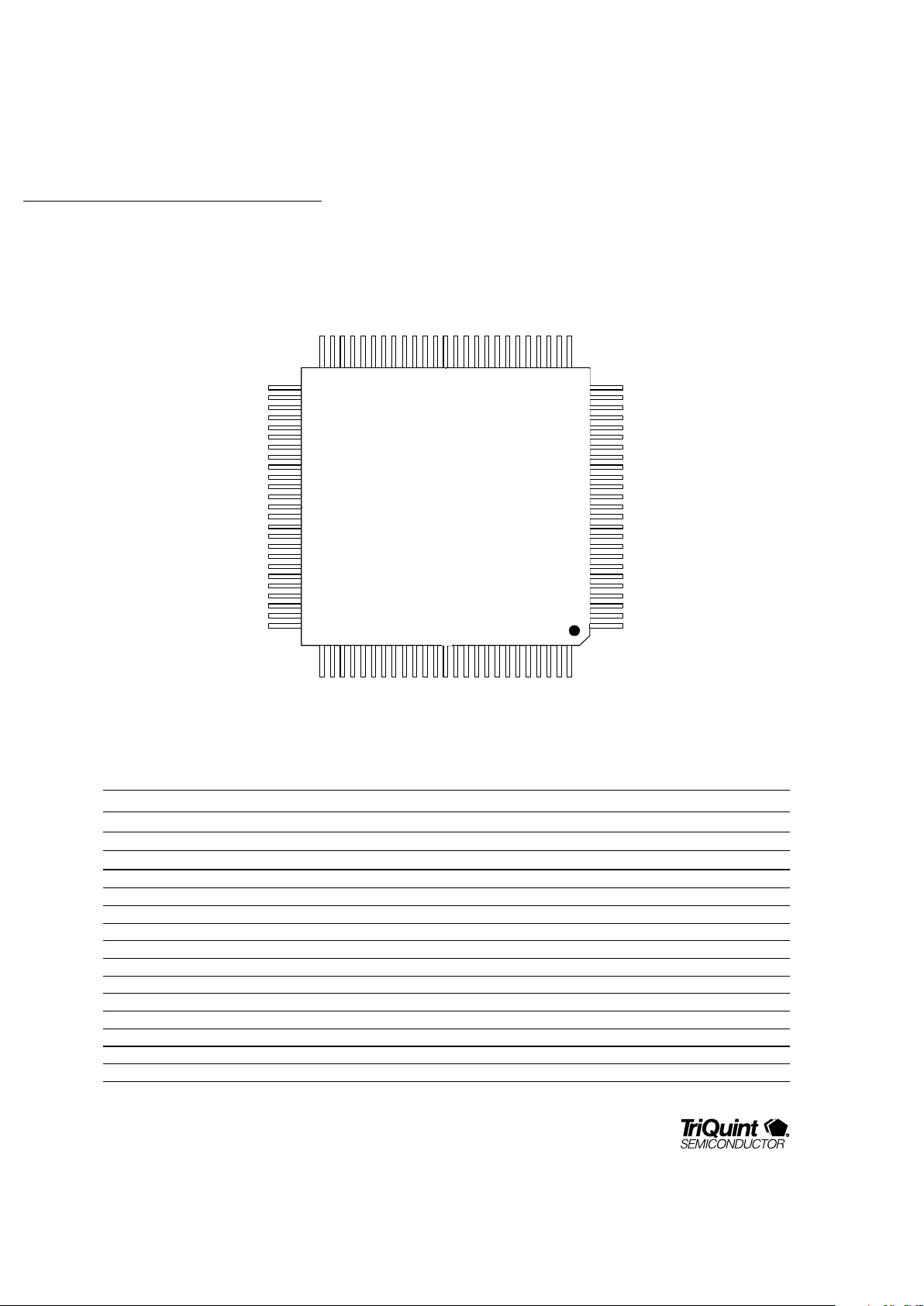
Figure 3. 100-Pin Enhanced Plastic 14x14 mm Package Pinout
Table 1. Signal Descriptions (continues on next page)
Pin Signal Function Description
1 VNN –5.2V/Ground ECL/PECL section power
2 NC No Connect Do not connect
3 VPP Ground/+5V ECL/PECL Positive Supply (see Table 6B)
4 DVPP Ground/+5V ECL/PECL Driver Return (see Table 6B)
5 REFCKEN ECL/PECL Input Tx Ref. Clock or Bypass Clock, Complement
6 REFCKEP ECL/PECL Input Tx Ref. Clock or Bypass Clock, True
7 DVPP Ground/+5V ECL/PECL Driver Return (see Table 6B)
8 TXCKN ECL/PECL Out Transmit Clock, Complement
9 TXCKP ECL/PECL Out Transmit Clock, True
10 DVPP Ground/+5V ECL/PECL Driver Return (see Table 6B)
11 TXDN ECL/PECL Out Transmit Data, Complement
12 TXDP ECL/PECL Out Transmit Data, True
13 DVPP Ground/+5V ECL/PECL Driver Return (see Table 6B)
14 RXDN ECL/PECL Input Receive Data, Complement
15 RXDP ECL/PECL Input Receive Data, True
Note: *TQ8106-specific signal
Note: *TQ8106-specific signal
13
TXDP
14
15
12
TXDN
11
DVPP
18
RXDP
19
DVPP
20
RXCKP
17
RXDN
16
DVPP
23
NSOL
24
VNN
25 GND
22
DVPP
21
RXCKN
8
DVPP
9
TXCKN
10
TXCKP
7
63REFCKEP
4
VPP
5
REFCKEN
21NC
38
DXD2
39
DGND
40
DXD337VCC36DXD1
43
DGND
44
DXD5
45 VCC
42 DXD4
41
VCC
48 DXD7
49 SVDD
50
VDD47DGND
46 DXD6
33 VCC
34 DXD0
35 DGND
32
DXSYNC
31 DGND
28
NC/CDRAVDD*29VCC30RXBC
27 VDD
26
SVDD
63
VDD
62
LBM0
61
GND
64
NOE
65
GND
58
RLOCK
57
56
CLRLOS
59
CDRGND*/NC
60
LBM1
53
VCC
52
OOF
51
GND
54
LOS
55
DGND
68
MMS
67
OC3
66
NRESET
69
CKSRC2
70
CKSRC1
73
PH0
72
PH1
71
CKSRC0
74
VDD
75
SVDD
88
DGND
87
TXBC
86
VCC
89
SONETCK
90
VCC
83
MXD5
82
MXD4 81
MXD384MXD685MXD7
78
MXD0 77
76
79
MXD180MXD2
93
LOR
92
DGND
91
SDHCK
94
AGND
95
FP2
98
VDD
97
AVDD
96
FP1
99
REFCKT
100
GND
DVPP
NC/CDRFP2*
NC/CDRFP1*
VPP
GND
VNN
FRPWR
NCDREN*/NC
Page 5
TQ8105/TQ8106
5
PRODUCTS
PRELIMINARY DATA SHEET
For additional information and latest specifications, see our website: www.triquint.com
TELECOM
PRODUCTS
Table 1. Signal Descriptions (continued)
Pin Signal Function Description
16 DVPP Ground/+5V ECL/PECL Driver Return (see Table 6B)
17 RXCKP ECL/PECL Input Receive Clock, True (Ignored when CDR used)
18 RXCKN ECL/PECL Input Receive Clock, Complement (Ignored when CDR used)
19 DVPP Ground/+5V ECL/PECL Driver Return (see Table 6B)
20 VPP Ground/+5V ECL/PECL Positive Supply (see Table 6B)
21 NSOL ECL/PECL Input Loss of Signal — zeroes serial data in when low; RXBC=TXCK/8
22 VNN –5.2V/Ground ECL/PECL section power (see Table 6B)
23 NC/CDRFP1* Analog Output CDR Loop Filter Pin 1 — Charge Pump Out (ignored by TQ8105)
24 NC/CDRFP2* Analog Input CDR Loop Filter Pin 2 — VCO Tune (ignored by TQ8105)
25 GND GND Core Ground
26 SVDD +5V Output Driver Internal Positive Supply
27 VDD +5V Core Positive Supply
28 CDRAVDD* Analog +5V TQ8106 CDR Analog +5V Supply
(not connected if CDR not used; ignored by TQ8105)
29 VCC +5V/+3.3V TTL Driver Positive Supply
30 RxBC Tristate TTL Out Demultiplexer Byte Clock
31 DGND GND TTL Driver Ground
32 DXSYNC Tristate TTL Out Frame Synchronization Signal
33 VCC +5V/+3.3V TTL Driver Positive Supply
34 DXD0 Tristate TTL Out Demultiplexer Data Bit 0 (LSB)
35 DGND GND TTL Driver Ground
36 DXD1 Tristate TTL Out Demultiplexer Data Bit 1
37 VCC +5V/+3.3V TTL Driver Positive Supply
38 DXD2 Tristate TTL Out Demultiplexer Data Bit 2
39 DGND GND TTL Driver Ground
40 DXD3 Tristate TTL Out Demultiplexer Data Bit 3
41 VCC +5V/+3.3V TTL Driver Positive Supply
42 DXD4 Tristate TTL Out Demultiplexer Data Bit 4
43 DGND GND TTL Driver Ground
44 DXD5 Tristate TTL Out Demultiplexer Data Bit 5
45 VCC +5V/+3.3V TTL Driver Positive Supply
46 DXD6 Tristate TTL Out Demultiplexer Data Bit 6
47 DGND GND TTL Driver Ground
48 DXD7 Tristate TTL Out Demultiplexer Data Bit 7 (MSB)
49 SVDD +5V Output Driver Internal Positive Supply
50 VDD +5V Core Positive Supply
51 NC/CDRGND* GND GND for TQ8106 to powerup CDR (ignored by TQ8105)
52 GND GND Core Ground
53 FRPWR TTL Input Framer Power Control (power on when high)
54 OOF TTL Input Out-of-Frame: Initiates Frame Search/Bit Alignment
55 VCC +5V/+3.3V TTL Driver Positive Supply
56 LOS Tristate TTL Output Loss of Signal (high when > 128 bit periods without transitions)
57 DGND GND TTL Driver Ground
Note: *TQ8106-specific signal
Page 6

6
TQ8105/TQ8106
PRELIMINARY DATA SHEET
For additional information and latest specifications, see our website: www.triquint.com
Table 1. Signal Descriptions (continued)
Pin Signal Function Description
58 CLRLOS TTL Input Active-high Clear LOS output
59 RLOCK Tristate TTL Output Receive Clock meets lock criteria when high
60 LBM1 TTL Input Loopback Mode Control (see Table 3)
61 GND GND Core Ground
62 LBM0 TTL Input Loopback Mode Control (see Table 3)
63 VDD +5V Core Positive Supply
64 NOE TTL Input TTL tristate control (active low to enable)
65 GND GND Core Ground
66 NRESET TTL Input Global Reset (active low)
67 OC3 TTL Input OC3/OC12 Mode Select
68 MMS TTL Input Master/Slave Mode Control
69 CKSRC2 TTL Input Clock Source Select (see Table 3)
70 CKSRC1 TTL Input Clock Source Select (see Table 3)
71 CKSRC0 TTL Input Clock Source Select (see Table 3)
72 PH1 TTL Input TxBC Phase Select (see Table 3)
73 PH0 TTL Input TxBC Phase Select (see Table 3)
74 VDD +5V Core Positive Supply
75 SVDD +5V Output Driver Internal Positive Supply
76 GND GND Core Ground
77 MXD0 TTL Input Multiplexer Data Bit 0 (LSB)
78 MXD1 TTL Input Multiplexer Data Bit 1
79 MXD2 TTL Input Multiplexer Data Bit 2
80 MXD3 TTL Input Multiplexer Data Bit 3
81 MXD4 TTL Input Multiplexer Data Bit 4
82 MXD5 TTL Input Multiplexer Data Bit 5
83 MXD6 TTL Input Multiplexer Data Bit 6
84 MXD7 TTL Input Multiplexer Data Bit 7 (MSB)
85 VCC +5V/+3.3V TTL Driver Positive Supply
86 TxBC Tristate TTL Out Transmit Byte Clock
87 DGND GND TTL Driver Ground
88 SONETCK Tristate TTL Out 51.84 MHz Clock Output
89 VCC +5V/+3.3V TTL Driver Positive Supply
90 SDHCK Tristate TTL Out 38.88 MHz Clock Output
91 DGND GND TTL Driver Ground
92 LOR Tristate TTL Out Indicates Reference Clock is Absent
93 AGND Analog Ground VCO Analog Ground
94 FP2 Analog Output Transmit PLL Loop Filter, Charge Pump Out
95 FP1 Analog Input Transmit PLL Loop Filter, VCO Tune
96 AVDD Analog +5V VCO & Filter Analog VDD Supply
97 VDD +5V Core Positive Supply
98 REFCKT TTL Input Tx Reference Clock or Bypass Clock
99 GND GND Core Ground
100 NC/NCDREN* TTL Input Internal Pull-up, Low = CDR receiver clock; Float = Pin 17/18 Rx Clk
(ignored by TQ8105)
Note:*TQ8106-specific signal
Page 7

TQ8105/TQ8106
7
PRODUCTS
PRELIMINARY DATA SHEET
For additional information and latest specifications, see our website: www.triquint.com
TELECOM
PRODUCTS
Function Description
PLL
The TQ8105 & TQ8106 incorporate high-stability, lowjitter Phase Locked Loops (PLLs) running at 2488.32
MHz. The PLLs use external surface mounted loop filters
consisting of an RC network as shown in the diagrams
that accompany the values shown in Table 2. Analog
design principles should be applied to the loop filter
portions of the circuit to ensure optimal jitter generation
performance. To reduce cross-coupling of clocks, both
CDR clocks and analog pins should be isolated from the
transmit PLL clock and analog pins. An analog ground
plane under the two capacitors and the resistor, along
with guards around the filter pins is excellent practice, as
is a well-filtered analog supply (AVDD) and a clean
analog ground (AGND). The loop filter values specified in
this preliminary data sheet may change.
Reference clock sourcing can be through a variety of
mechanisms. As shown in Table 3, the MMS pin
determines whether the device operates in Master
mode (where the PLL reference comes in on either a
TTL or PECL/ECL pin), or a Slave mode (where the PLL
reference is derived from the DEMUX high-speed line
clock input). If the external reference clock pins are
used, note that they are logical ORs and that the
unused pin should be tied to (a) GND for unused
REFCKT, or (b) REFCKEN should be tied to VPP for TTL
reference operation. The reference clock frequency can
be selected from any number of values, as indicated in
Table 3. Note that the PLL may be bypassed, allowing
use of an external clock reference.
Internal dividers determine the operating line rate, as
shown in Table 3. The device is capable of operating at
STM1/STS-3 or STM4/STS-12 rates. The transmit PLL
provides high performance and compliance with ITU/
Bellcore requirements found in the first-generation
TQ8101. The TQ8106 receiver's CDR can be disabled
for backwards pin-compatibility with the TQ8105. For
circuits not requiring the TQ8106's CDR, the CDR is
disabled by floating NCDREN (pin 100). Further, the CDR
section of the TQ8106 can be powered down by
disconnecting the CDRGND and CDRAVDD pins, thereby
reducing power consumption. If the TQ8106 CDR is not
used, the CDR filter pins may be left unconnected.
The transmit PLL also provides constant-rate 38.88 MHz
and 51.84 MHz TTL outputs which may be tristated. The
38.88 MHz & 51.84 MHz output may also be achieved by
using high-speed receiver timing in Clock Source Mode
011 (see Table 3).
Framer
The TQ8105 and TQ8106 provide a clean interface to
devices from PMC-Sierra and others. The Out-of-Frame
(OOF) input is a state (level)-initiated event, rather than
the edge-triggered event found on TriQuint’s firstgeneration TQ8101 transceiver. When OOF is high, the
TQ8105/TQ8106 initiates a frame search for a serial bit
pattern of twelve A1s (three A1s in OC3 mode)
followed
by three A2s. If a match occurs, the device realigns
byte boundaries and issues a logic high on the DXSYNC
pin during the third A2. In the absence of OOF,
the
device will not realign byte boundaries, but will report
any bit-level matching of twelve A1s (three A1s in OC3
mode) followed by three A2s as a DXSYNC pulse.
Framer circuit power may be switched off by a TTL low on
the FRPWR pin, saving approximately 0.25W. No further
DXSYNC pulses will be issued, though bit alignment is
preserved in the demux. Note that the OOF and FRPWR
pins may be tied together, powering the framer only when
bit realignment is required (this is not recommended
practice, however, due to the inrush currents that may
result).
Loopbacks
As part of the TQ8105 and TQ8106 on-chip diagnostics,
four loopback modes are supported. These are selected
by the dedicated pins LBM0 and LBM1, as shown in
Table 3. The loopback modes are shown in Figure 5.
Page 8

8
TQ8105/TQ8106
PRELIMINARY DATA SHEET
For additional information and latest specifications, see our website: www.triquint.com
Functional Description (continued)
Enhanced Diagnostics
The TQ8105 and TQ8106 incorporate on-chip clock
diagnostics, allowing fast, efficient fault detection and
isolation at the systems level.
The LOR (Loss Of Reference) output goes high when the
reference clock is absent. Note that this signal is not
latched and is only high when the reference clock is
missing. A reference clock is required for the TQ8106
CDR to function correctly.
The NSOL (Loss-of-signal input, active low, PECL/ECL
level) input allows the receiver to force zeroes onto the
demux outputs. A TTL-level signal may also be used for
NSOL if the resistor network, shown in the applications
section of this data sheet, is used. NSOL is useful when a
Loss Of Signal occurs on the receive optics, and a
quieting of invalid data is desired. The receiver is clocked
from the transmit clock when NSOL is active, and the
output RXBC clock is obtained from the transmit portion
of the TQ8105/TQ8106. This ensures compatibility with
devices, such as the PMC-Sierra S/UNI-622 and STTX
components, which may contain dynamic registers that
lose contents if clocks are removed. NSOL forces the
CDR to lock on REFCLK, except when in slave mode.
The LOS (Loss Of Signal) output goes high whenever
128-bit periods occur without transitions on the data
input to the demux. CLRLOS forces LOS low.
The RLOCK (Receiver LOCK) output goes low whenever the
signal on RXCK or the recovered clock drifts more than
500 ppm from the reference frequency. This output returns
high whenever the frequency accuracy is within 100 ppm.
Demux
The TQ8105/TQ8106 demultiplexer converts an NRZ
PECL/ECL data input, at either 155 Mb/s or 622 Mb/s,
and its corresponding PECL/ECL clock into a byte-
parallel
78 MHz or 19 MHz tristatable TTL data bus. The timing is
shown in Figures 6 through 8. See the previous “Framer”
description for bit alignment details. The TQ8106 can
recover both clock and data from a NRZ data stream,
whereas the TQ8105 requires NRZ data and a recovered
clock.
Mux
The TQ8105/TQ8106 multiplexer converts a 78 MHz or
19 MHz byte-wide bus to a serial NRZ PECL/ECL data
stream. The bytes are clocked into the device with the
TXBC byte clock output. The timing is shown in Figures
6 through 8. Note that the TXBC output can be adjusted
in 90-degree phase increments to accommodate
variations in interface requirements. See Table 3 for
settings on the PH0 and PH1 pins controlling this
function. Data may also be clocked into the TQ8105/
TQ8106 by a 77 MHz reference, oscillator-clock source,
provided the data is within the timing limits shown in the
timing diagram labelled “Reference Clock Based
Transmit Timing.” The TQ8105 and TQ8106 do not
require the transmit latch found on earlier TQ8101
reference designs and are backwards compatible with
designs that have the latch incorporated.
High-Speed I/O and TTL Interfaces
The TQ8105/06P will operate with either PECL or ECL
operation on the high-speed I/O. With a single +5V
supply, the part interfaces directly with TTL and PECL
(Positive Emitter Coupled Logic). By providing an
additional -5.2V supply, the device’s high-speed I/O
becomes ECL, instead of PECL. The TQ8105/06S is
designed only for PECL high-speed I/0 operation with a
single +5V supply. The power supply connections for
PECL and ECL are shown in Table 6B.
The TTL outputs (Vcc) may be connected to either +5V or
+3.3V supplies. True TTL may be obtained with the +5V
connection; clamped operation, when connected to +3.3V,
ensures that maximum Voh levels do not exceed +3.3V.
Page 9

TQ8105/TQ8106
9
PRODUCTS
PRELIMINARY DATA SHEET
For additional information and latest specifications, see our website: www.triquint.com
TELECOM
PRODUCTS
TQ8105/TQ8106 Design Notes
These design notes are provided to assist the circuit
designer in achieving the highest possible performance
while reducing design time. Unless noted otherwise,
references to the TQ8105 apply equally to the TQ8106.
Interfacing to PMC-Sierra Devices
The transmit timing of the TQ8105 is such that the
PMC-Sierra byte outputs (POUT(0:7)) may be directly
connected to the TQ8105 mux inputs (MXD(0:7)). The
TQ8105 uses an Out-Of-Frame (OOF) input as a signal
to reframe while high, allowing direct connection of the
PM5355's OOF output to the TQ8105 OOF input. The
following summarizes connectivity between the devices.
PM5355 TQ8105/TQ8106
POUT(0:7) MXD(0:7)
PIN(0:7) DXD(0:7)
OOF OOF
PICLK RXBC
FPIN DXSYNC
TCLK TXBC
POP(0:5) Any TQ8105 modes to be programmable
PIP(0:3) Any TQ8105 diag outputs to be readable
Reference Design
A reference design (see Figure 4) and evaluation board
are available from TriQuint. They incorporate a 1x9 or
2x9 fiber optic transceiver (with the option of clock
recovery), the PM5355 PMC Sierra framer device, and
a TQ8105 or TQ8106.
Thermal Considerations
Figure 9 shows the region where the use of a heatsink is
not required. For example, the TQ8105 does not require
a heatsink for ambient temperatures up to 55°C in still
air. An airflow of 100 LFPM raised this temperature to
approximately 75°C, eliminating heatsink requirements.
In applications requiring a heatsink, a standard pin-fin
heat-sink is appropriate. To attach the sink, use spring
clips soldered to the board to cross and hold the
heatsink. The clip holes in the board are at the corners of
a 1.275” x 1.5” rectangle. Another alternative is the
circular heatsink, #2288B from Thermalloy attached with
their Thermattach #19686-3.
Power Supplies
Good decoupling practices should be observed, with a
0.1 uF decoupling capacitor at each supply pin, ideally
on the component side of the board.
Keep the analog
supplies (Vdd and AVdd) pristine.
Proper design will
isolate the supply groups using point grounding to tie
supplies together (
all
grounds at a single point having
multiple vias).
For the analog supply, flood copper under the loop filter
on the component side of the board, tying the flood to
the analog ground pin, with the point ground away from
the filter and analog pin, so that any switching currents
are kept away from these areas. If any switching,
power-supply frequencies below 500 kHz are used in
the system, use a supply filter on the analog supply pin.
These practices help minimize the generation of jitter.
High-Speed Connections
Connections to E/O modules (and clock reference, if
used) are direct-coupled PECL and need to be terminated
with decoupled 50 ohms to 3V at the receiving end of the 50
ohm transmission line. Ensure that each 50 ohm resistor
(or Thevenin equivalent) has its own decoupling
capacitor. Place the resistor at the end of a 50 ohm
transmission line (use a controlled impedance layer),
ideally with a minimal-length stub attached to either the
resistor or the receiving device.
If there is no room for the resistor, use a minimallength stub to drop the signal at the receiving device
pins, continue the 50 ohm transmission line to an area
where the termination resistors can be placed, and
terminate at the endpoint of that line. If in doubt,
contact factory applications for assistance.
Page 10

10
TQ8105/TQ8106
PRELIMINARY DATA SHEET
For additional information and latest specifications, see our website: www.triquint.com
10
0.1u
gnd_s
330
220
VDD
gnd_s
VDD
gnd_s
330
220
PIN0
148
PIN1
147
PIN2
146
PIN3
145
PIN4
144
PIN5
143
PIN6
142
PIN7
141
FPIN
149
FPOS
150
PICLK
137
TLAIS
88
TSD
103
TSOW
94
TSUC
93
TLRDI
89
TLD
91
TLOW
92
TTOH1
86
TTOH2
85
TTOH3
84
TTOH4
83
TTOHEN
101
TPOH
82
TPOHEN
77
TPAIS
73
TPRDI
72
RSICLK
139
RSIN
140
TSICLK
104
TFCLK
65
XOFF
63
TSOC
60
TXPRTY0
58
TXPRTY1
59
TWRENB
61
TDAT0
42
TDAT1
43
TDAT2
44
TDAT3
45
TDAT4
46
TDAT5
47
TDAT6
48
TDAT7
49
TDAT8
50
TDAT9
51
TDAT10
52
TDAT11
53
TDAT12
54
TDAT13
55
TDAT14
56
TDAT15
57
RRDENB
186
RFCLK
190
TSEN
192
TGFC
62D0 23D1 24D2 25D3 26D4 31D5 32D6 33D7 34A0 15A1 16A2 17A3 18A4 19A5 20A6 21A7 22
ALE
14
CSB
36
WRB
37
RDB
38
RSTB
35
TCK
70
TMS
126
TDI
127
TDO
71
TRSTB
125
FPOUT
123
POUT0
122
POUT1
121
POUT2
116
POUT3
115
POUT4
114
POUT5
113
POUT6
112
POUT7
111
OOF
164
LOF
163
LOS
169
TSDCLK
102
TOWCLK95RSDCLK
159
RSD
160
ROWCLK
168
RSOW
162
RSUC
161
OHFP
175
LAIS
171
LRDI
170
RLDCLK
173
RLD
172
RLOW
167
TLDCLK
90
RTOH1
156
RTOH2
155
RTOH3
154
RTOH4
153
RTOHCLK
157
RTOHFP
158
TTOHCLK
99
TTOHFP
100
RPOH
181
RPOHCLK
176
RPOHFP
177
TPOHCLK
75
TPOHFP
76
LOP
178
PAIS
182
PRDI
185
TSOUT
124
GTOCLK87GROCLK
174
LCD
188
RSOC
195
RXPRTY0
196
RXPRTY1
197
RDAT0
198
RDAT1
199
RDAT2
200
RDAT3
201
RDAT4
202
RDAT5
203
RDAT6
204
RDAT7 1RDAT8 2RDAT9
3
RDAT10 4RDAT11 5RDAT12 6RDAT13 7RDAT14 8RDAT15
9
RCA
194
TCA67RCP
187
RGFC
193
TCP
68
POP0
135
POP1
134
POP2
133
POP3
132
POP4
131
POP5
130
PIP0
108
PIP1
107
PIP2
106
PIP3
105
INTB
39
VDD_AC1
1
0
VDD_AC2
2
7
VDD_AC3
8
1
VDD_AC4
120
VDD_AC5
152
VDD_AC6
183
VDD_AC7
205
VDD_DC1
1
1
VDD_DC2
2
8
VDD_DC3
4
0
VDD_DC4
6
6
VDD_DC5
8
0
VDD_DC6
9
8
VDD_DC7
110
VDD_DC8
119
VDD_DC9
129
VDD_DC1
0
138
VDD_DC1
1
165
VDD_DC1
2
179
VDD_DC1
3
189
VDD_DC1
4
206
TCL
K
9
7
TFP
7
4
VSS_AC1
1
3
VSS_AC2
3
0
VSS_AC3
7
8
VSS_AC4
117
VSS_AC5
151
VSS_AC6
184
VSS_AC7
208
VSS_DC1
1
2
VSS_DC2
2
9
VSS_DC3
4
1
VSS_DC4
6
4
VSS_DC5
7
9
VSS_DC6
9
6
VSS_DC7
109
VSS_DC8
118
VSS_DC9
128
VSS_DC1
0
136
VSS_DC1
1
166
VSS_DC1
2
180
VSS_DC1
3
191
VSS_DC1
4
207
NC6
9
6
9
U?
S/UNI 622
VDD
gnd_s
VDD
8141
7
U?
77.76M Osc
gnd_s
0.1u
MXD0
77
MXD1
78
MXD2
79
MXD3
80
MXD4
81
MXD5
82
MXD6
83
MXD7
84
OOF
54
DXD034DXD136DXD238DXD340DXD442DXD544DXD646DXD7
48
DXSYNC
32
RXBC30TXBC
86
REFCKT
98
REFCKEP
6
REFCKEN
5
RXDP
15
RXDN
14
RXCKP
17
RXCKN
18
NSOL
21
PH0
73
PH1
72
CKSRC0
71
CKSRC1
70
CKSRC2
69
LBM0
62
LBM1
60
MMS
68
OC3
67
CLRLOS
58
FRPWR
53
NOE
64
NRESET
66
LOR
92
FP195FP2
94
AVDD96AGND
93
NCI_1
100
NCI_551NCI_428NCI_324NCI_2
23
LOS
56
RLOCK
59
GND_1
2
5
GND_2
5
2
GND_3
6
1
GND_4
6
5
GND_5
7
6
GND_6
9
9
DGND_
1
3
1
DGND_
2
3
5
DGND_
3
3
9
DGND_
4
4
3
DGND_
5
4
7
DGND_
6
5
7
DGND_
7
8
7
DGND_
8
9
1
VDD_1
2
7
VDD_2
5
0
VDD_3
6
3
VDD_4
7
4
VDD_5
9
7
SVDD_
1
2
6
SVDD_
2
4
9
SVDD_
3
7
5
VCC_1
2
9
VCC_2
3
3
VCC_3
3
7
VCC_4
4
1
VCC_5
4
5
VCC_6
5
5
VCC_7
8
5
VCC_8
8
9
VNN_1
1
VNN_2
2
2
SDHCK
90
SONETCK
88
VPP_1
3
VPP_2
2
0
DVPP_1 4DVPP_2 7DVPP_310DVPP_413DVPP_516DVPP_6
19
TXDP
12
TXDN
11
TXCKP 9TXCKN
8
U?
TQ8105
VDD
1uH
1uH
gnd_s
gnd_s
gnd_s
VDD
0.1u
0.1u
10u
0.1u 0.1u
VDD
gnd_s
REFCLK
1
LCKREFN
2
TXVCC
1
3
RXVCC
1
4
RXVEE
1
8
TXVEE
1
0
TD
11
TDN
12
SD
15
CLKN
3
CLK 4RDN
16RD17
U?
HFBR5207
82
130
82
0.1u
gnd_s
VDD
*Note 1
130
UTOPIA
*Note 4
VDD
330
330
330
gnd_s
VDD
VDD
*Note 2
*330
*330
*330
*330
gnd_s
*Note 3
330
VDD
VDD
gnd_s
VDD
4.7K
*0
gnd_s
0.1u
R1
10u
C1
C2
gnd_s
gnd_s
1uH
gnd_s
VDD
0.1u
VDD
1uH
0.1u
R2
C4
10u 10u
0.1u
C3
Note: See Tables 2A & 2B
for loop filter values.
gnd_s
VDD
2K
2K
82 82
82 82
VDD
20K
*Note 1
470
470 470
gnd_s
Notes:
1) Place termination networks as close to
their respective input pins as possible.
2) Setting of PH(0:1) is board-layout dependent.
These 4 resistors are used as placeholders
for the appropriate strapped settings that
are determined at initial board evaluation.
(See Table 3 and associated text.)
3) Install 0-ohm resistor for TQ8106 operation.
4) May use SONETCK (51.84MHz) for
UTOPIA bus clock.
gnd_s
VDD
NLOCKED
LOSLOR
130
130
0.1u
130
130
gnd_s
gnd_s
10u
VDD
TQ8105 Decoupling
0.1u
gnd_s
(Decoupling not shown for PM5355)
*Only connections pertinent to the TQ8105/06
to S/UNI overhead processor chip are shown.*
10u
0.1u 0.1u
10u
0.1u
0.1u
0.1u
0.1u
VDD
VDD
0.1u 0.1u
0.1u 0.1u
0.1u
0.1u 0.1u
0.1u
0.1u
0.1u 0.1u
0.1u
gnd_s
gnd_s
gnd_s
Reset
gnd_s
47u
gnd_s
10K
VDD
330
Figure 4. Reference Design Schematic
Page 11

TQ8105/TQ8106
11
PRODUCTS
PRELIMINARY DATA SHEET
For additional information and latest specifications, see our website: www.triquint.com
TELECOM
PRODUCTS
Table 2B. TQ8106 Recommended CDR Loop Filter Values
(Preliminary)
Incoming Resistor Capacitor Capacitor
NRZ Data Rate Value R2 Value C3 Value C4
(Mbs) (ohms) (µF) (pF)
155.52 470 1.0 39
622.08 680 4.7 39
RXD
DXD
TXD
TXCK
RXBC
MXD
Normal
Equipment
RXD
DXD
RXBC
MXD
RXCK
TXCK
TXCK
TXCK
TXD
TXDTXD
MXD
DXD
RXD
RXD
DXD
RXCK
RXCK
Split
Facility
MXD
RXBC
RXCK
Figure 5. Loopback Modes
Table 2A. TQ8105/TQ8106 Recommended Transmit Loop Filter Values (Preliminary)
Reference Resistor Capacitor Capacitor
Frequency Divide Value R1 Value C1 Value C2
(MHz) Ratio (ohms) (µF) (pF)
19.44 32 1200 0.082 82
38.88 16 620 0.15 150
51.84 12 470 0.22 220
77.76 8 300 0.33 330
155.52* 4 300 0.33 330
Note: *Internal divide by two on Reference
CDRFP2
CDRFP1
CDRAVDDAVDD
FP2
FP1
C2
C1
R1
C3
R2
C4
Page 12

12
TQ8105/TQ8106
PRELIMINARY DATA SHEET
For additional information and latest specifications, see our website: www.triquint.com
Table 3. Mode Selection
Signals Mode
LBM(1:0) Loopback: 00 = Normal, 01 = Equipment, 10 = Facility, 11 = Split
PH(1:0) 00 = 0 degrees delay, 01 = 90 degrees delay, 10 = 180 degrees delay, 11 = 270 degrees delay
MMS 1 = Master (use REFCKT/E as reference), 0 = Slave (use receive clock as reference)
CKSRC(2:0) Clock Source: 000 = PLL bypass
001 = 51.84 MHz PLL reference, SONETCK & SDHCK tristate
010 = 155.52 MHz PLL reference
011 = 51.84 MHz PLL reference, SONETCK=8, SDHCK derived from receiver timing
100 = 77.76 MHz PLL reference
101 = 51.84 MHz PLL reference
110 = 38.88 MHz PLL reference
111 = 19.44 MHz PLL reference
OOF 1 = Initiate frame search, 0 = Do not permit reframing (see FRPWR pin in Table 1)
NSOL 1 = Pass receive data, 0 = Force receive data to 0
OC3 1 = Operate at STM1/STS-3 (or PLL bypass divided by 4), 0 = Operate at STM4/STS-12/PLL bypass
NRESET 1 = Normal operation, 0 = Reset internal counters
NCDREN 1 = TQ8105/CDR Off mode, 0 = Enable CDR (TQ8106 only)
Table 4. Absolute Maximum Ratings
Parameter Symbol Level Minimum Maximum Unit
Positive supply V
CC, VPP
, V
DD, AVDD
GND 7 V
Negative supply (VPP = 0 V) V
NN
–7 GND V
Output voltage V
O
ECL/PECL VNN–0.5 VPP+0.5 V
Output current I
O
ECL/PECL — 40 mA
Input voltage V
I
ECL/PECL VNN–0.5 VPP+0.5 V
Input current I
I
ECL/PECL –1 1 mA
Output voltage V
O
TTL –0.5 VCC+0.5 V
Output current I
O
TTL — 100 mA
Input voltage V
I
TTL –0.5 VCC+0.5 V
Input current I
I
TTL –1 1 mA
Biased junction temperature T
J
— –55 +150 ° C
Storage temperature T
S
— –65 +150 ° C
Page 13

TQ8105/TQ8106
13
PRODUCTS
PRELIMINARY DATA SHEET
For additional information and latest specifications, see our website: www.triquint.com
TELECOM
PRODUCTS
Table 6A. Recommended Operating Conditions
Parameter Symbol Minimum Typical Maximum Unit
Positive supply V
PP
4.75 5.0 5.25 V
Output driver positive supply V
CC
3.0 5.25 V
Negative supply (ECL mode only) V
NN
–5.5 –5.2 –4.75 V
Operating case temperature (see Figure 9) –40 125 °C
Table 6B. Power Supply Connections
Pin +5V TTL/PECL I/O +3.3V TTL/PECL I/O +5V TTL/ECL I/O +3.3V TTL/ECL I/O
VDD +5V +5V +5V +5V
SVDD +5V +5V +5V +5V
VCC +5V +3.3V +5V +3.3V
AVDD Filtered +5V Filtered +5V Filtered +5V Filtered +5V
CDRAVDD Filtered +5V Filtered +5V Filtered +5V Filtered +5V
GND 0V (ground) 0V (ground) 0V (ground) 0V (ground)
AGND 0V (ground) 0V (ground) 0V (ground) 0V (ground)
CDRGND 0V (ground) 0V (ground) 0V (ground) 0V (ground)
VPP/DVPP +5V +5V 0V (ground) 0V (ground)
VNN 0V (ground) 0V (ground) -5.2V -5.2V
Table 5. Power Consumption
Symbol Function Minimum Typical Maximum Unit
I
DD
+5V supply — 0.323 TBD I
I
CC
+5V / +3V supply — 0.016 TBD I
I
PP
+5V / 0V supply — 0.055 TBD I
I
ADD
+5V supply — 0.018 TBD I
P
DF
Power dissipation, Framer on, TQ8106 CDR off — 1.9 2.3 W
P
D
Power dissipation, Framer off, TQ8106 CDR off — 1.7 2.1 W
P Power dissipation, Framer on, TQ8106 CDR on 2.75 W
Page 14

14
TQ8105/TQ8106
PRELIMINARY DATA SHEET
For additional information and latest specifications, see our website: www.triquint.com
Table 8. DC Characteristics—TTL I/O
(Specifications apply over recommended operating ranges)
Parameter Condition Symbol Minimum Nominal Maximum Unit
Input HIGH voltage V
IH
2.0 — V
CC
V
Input LOW voltage V
IL
0 — 0.8 V
Input HIGH current V
IH(MAX)
I
IH
— — 200 uA
Input LOW current V
IL(MIN)
I
IL
–400 –200 — uA
Output HIGH voltage IOH = 50 mA V
OH
2.4 — V
CC
V
Output LOW voltage IOL = –20 mA V
OL
0 — 0.4 V
Tristate current I
OZ
–100 — 100 uA
Input capacitance C
IN
— — TBD pF
Output capacitance C
OUT
— — TBD pF
ESD breakdown rating (Design objective) V
ESD
Class I — —
Table 7. DC Characteristics—ECL/PECL I/O
(Specifications apply over recommended operating ranges).
Parameter Condition Symbol Minimum Nominal Maximum Unit
Internal ECL reference Single-ended inputs V
REF
— 0.26 V
NN
+ 0.74 V
PP
mV
Common mode voltage Differential inputs V
COM
V
PP
– 1500 — V
PP
– 1100 mV
Differential voltage Differential inputs V
DIFF
200 — 1200 mV
Input HIGH voltage V
REF
= 1300 mV V
IH
V
PP
– 1050 — V
PP
– 400 mV
Input LOW voltage V
IL
V
TT
—V
PP
– 1550 mV
Output HIGH voltage R
LOAD
= 50 ohms V
OH
V
PP
– 1000 V
PP
– 600 mV
to VTT = V
PP
– 2.0V
Output LOW voltage R
LOAD
= 50 ohms V
OL
V
TT
—V
PP
– 1600 mV
to VTT = V
PP
– 2.0V
Input HIGH current V
IH(MAX)
I
IH
— +130 335 uA
Input LOW current V
IL(MIN)
I
IL
–265 –130 — uA
Output HIGH current (Not tested; consistent I
OH
20 23 30 mA
with VOH and V
OL
tests)
Output LOW current (Not tested; consistent I
OL
058mA
with VOH and V
OL
tests)
Input capacitance C
IN
— — TBD pF
Output capacitance C
OUT
— — TBD pF
ESD breakdown rating (Design objective) V
ESD
Class I — —
Note: VTT = VPP-2.0V
Page 15

TQ8105/TQ8106
15
PRODUCTS
PRELIMINARY DATA SHEET
For additional information and latest specifications, see our website: www.triquint.com
TELECOM
PRODUCTS
Table 9. AC Characteristics
(Specifications apply over recommended operating ranges)
Parameter Symbol Minimum Nominal Maximum Unit
RXCK clock period T
C(RXCK)
1.6 — — ns
REFCKE clock period T
C(REFCKE)
1.6 — — ns
TXCK clock period T
C(TXCK)
1.6 — — ns
REFCKT clock period T
C(REFCKT)
12.8 — — ns
TXBC clock period T
C(TXBC)
12.8 — — ns
RXBC clock period T
C(RXBC)
12.8 — — ns
REFCKT/REFCKE clock duty cycle T
C(REF)
40 — 60 %
REFCKT to TXBC skew
2,3,5
T
SK(TXBC)
TBD TBD
SONETCK clock period T
C(SONETCK)
— 19.29 — ns
RXBC clock duty cycle
3,5
T
DC(RXBC)
40 50 60 %
TXBC clock duty cycle
3,5
T
DC(TXBC)
40 50 60 %
TXCK clock duty cycle
6
T
DC(TXCK)
40 50 60 %
SONETCK clock duty cycle
3,5
T
DC(SONETCK)
40 50 60 %
SDHCK clock duty cycle
3,5
T
DC(SDHCK)
40 50 60 %
RXCK clock duty cycle
6
T
DC(RXCK)
40 50 60
High-speed rise/fall time4 (> 79 MHz), Data T
H(R/F)
— — 500 ps
High-speed rise/fall time4 (>79 MHz), Clock T
H(R/F)
— — 320 ps
Low-speed rise/fall time
1,3,5
(< 79 MHz) T
L(R/F)
——3ns
RXD setup time to RXCK6 (see Figure 6) T
S(RXD)
240 — — ps
RXD hold time to RXCK6 (see Figure 6) T
H(RXD)
20 — — ps
OOF rising edge before A1 changes to A2
7
T
(OOFH)
51.44 — — ns
(see Figure 8)
DXSYNC rising edge from parallel data output T
(DSYNC)
— 25.72 — ns
change from A1 to A2
7
DXSYNC pulse width
3,5,7
(see Figure 8) T
(DXSYNCPW)
11.0 — — ns
RXBC falling edge to valid parallel data output
3
T
P(DXD)
0.5 1.0 ns
(see Figure 7)
MXD(0:7) setup time to TXBC
2,3,5
(see Figure 6) T
S(MXD)
600 — — ps
MXD(0:7) hold time to TXBC
2,3,5
(see Figure 6) T
H(MXD)
600 — — ps
TXCK falling edge to TXD6 (see Figure 7) T
P(TXD)
200 — 400 ps
220Ω
330Ω
18pF
V
cc
Notes: 1. At 0.8V/2.0V levels
2. With PH(1:0) set to 00, 18pF total loading
3. TTL outputs test load (V
CC
= +5V):
4. 20%/80%
levels
5. At 1.4V logic threshold level
6. Differential measurement
7. OC12 mode
Page 16

16
TQ8105/TQ8106
PRELIMINARY DATA SHEET
For additional information and latest specifications, see our website: www.triquint.com
TXCK
TXD
T
P(TXD)
RXBC
DXD(7:0)
T
P(DXD)
DXSYNC
T
P(DXSYNC)
Figure 7. Output Timing
Figure 6. Input Timing
RXCKP
RXD
T
S(RXD)
T
H(RXD)
TXBC
MXD(7:0)
T
S(MXD)
T
H(MXD)
Page 17

TQ8105/TQ8106
17
PRODUCTS
PRELIMINARY DATA SHEET
For additional information and latest specifications, see our website: www.triquint.com
TELECOM
PRODUCTS
Figure 8. Demultiplexer Timing
OOF
DXSYNC
RXD
RXBC
DXD(7:0)
RXCK
RXBC Resync
T
(DXSYNCPW)
T
(OOFH)
A1
#1
A1#2A1
#
n
A2#1A2#2A2
#3
A1
#
n
-2
A1
#
n
-1A1#
n
A2#1A2#2A2
#3
Figure 9. Required Airflow for Operation without Heatsink
100
90
80
70
60
50
40
30
0 100 200 300 400 500 600
TQ8105
TQ8106
Required airflow (LFPM)
Maximum ambient air temperature (˚C)
Page 18

18
TQ8105/TQ8106
PRELIMINARY DATA SHEET
For additional information and latest specifications, see our website: www.triquint.com
.25
2
1
N
1
1
1
L
A
D
D
E
E
A
A
A
e
b
A
1
Standoff
.17 max.
A
B
D
SD
S
A-B
C
M
ddd
Lead Coplanarity
Exposed Heatsink
6.86 ± .50 dia.
Heatsink Intrusion
.0127 max.
C
Seating
Plane
C
ccc
Figure 10. Mechanical Package (100 pins, 14 x 14 mm)
Package Package “P”
1
Package “S”
Dimension Value
2
Value
2
A 2.35 1.7 max
A
1
0.25 max 0.10
A
2
2.00 1.40
D 17.20 ±0.25 16.00 ±0.4
D
1
14.00 14.00
E 17.20 ±0.25 16.00 ±0.4
E
1
14.00 14.00
L 0.88 +0.15/–0.10 0.50 ±0.20
b 0.22 0.18
e 0.50 0.50
N 100 pins 100 pins
Notes: 1. Not recommended for new designs.
2. All dimensions in millimeters (mm).
Page 19

TQ8105/TQ8106
19
PRODUCTS
PRELIMINARY DATA SHEET
For additional information and latest specifications, see our website: www.triquint.com
TELECOM
PRODUCTS
Ordering Information
TQ8105P
SONET/SDH Transceiver, PECL/ECL I/O
TQ8106P
SONET/SDH Transceiver w/CDR, PECL/ECL I/O
TQ8105S
SONET/SDH Transceiver, PECL I/O
TQ8106S
SONET/SDH Transceiver w/CDR, PECL I/O
Reference Designs
The following products are available for 14-day loan to qualified customers:
ATM SONET/SDH Line Interface Module (SLIM)
Supports OC12c/STM-4 (622.08 Mbps) and OC-3c/STM-1 (155.52 Mbps)
The information provided herein is believed to be reliable; TriQuint assumes no liability for inaccuracies or
omissions. TriQuint assumes no responsibility for the use of this information, and all such information
shall be entirely at the user's own risk. Prices and specifications are subject to change without notice.
No patent rights or licenses to any of the circuits described herein are implied or granted to any third party.
TriQuint does not authorize or warrant any TriQuint product for use in life-support devices and/or systems.
Copyright © 1998 TriQuint Semiconductor, Inc. All rights reserved.
Revision 0.3.A July 1998
Additional Information
For latest specifications, additional product information,
worldwide sales and distribution locations, and information about TriQuint:
Web: www.triquint.com Tel: (503) 615-9000
Email: sales@tqs.com Fax: (503) 615-8900
For technical questions and additional information on specific applications:
Email: applications@tqs.com
SLIM Documentation Package
• Functional Partition Drawing Set, including
block, state machine, and timing diagrams
• Schematics
• Programmable Logic Listings
• User’s Manual / Product Specification
• PCB Artwork (all layers)
• Component Placement Drawing
 Loading...