

Page 1
T R I Q U I N T S E M I C O N D U C T O R , I N C .
TQ8034
PRELIMINARY DATA SHEET
0:5
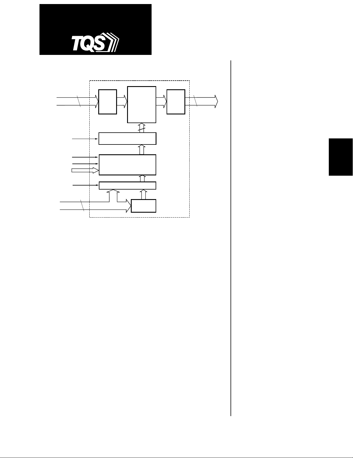
34 x 34
Crosspoint
Switch Matrix
6:34 Decoder
Output
Buffers
TQ8034
OUT0:33
68
IN0:33
CONFIGURE
LOAD
MODE(1)
IADD0:5
MODE(0)
OADD0:33
Input
Buffers
68
34 6-Bit Configuration Latches
34 6-Bit Program Latches
Output Address Select
0:33
34
The TQ8034 is a non-blocking 34 X 34 digital crosspoint switch capable of data
rates greater than 1.6 Gigabits per second per port. Utilizing a fully differential
data path from input to output, the TQ8034 offers a high data rate with
exceptional fidelity. The symmetrical switching and noise rejection
characteristics inherent in differential logic result in low jitter, low crosstalk and
minimum signal skew. The TQ8034 is ideally suited for gigabit data and HDTV
switching applications.
1.6 Gbit/sec
3.3V 34x34 Digital
Crosspoint Switch
Features
• >1.6 Gb/s port data bandwidth
>50 Gb/s aggregate bandwidth
• 3.3V power supply
• Fully differential data path for
superior signal fidelity
• Non-blocking architecture
• Full broadcast and multi-cast
capability
• Differential LVPECL I/O with
TTL control
• On-chip 50 Ohm LVPECL input
termination
• Low jitter and signal skew
• Two-stage configuration register
• Multiple programming modes
PRODUCTS
SWITCHING
The non-blocking architecture uses 34 fully independent 34:1 multiplexers,
allowing each output port to be independently programmed to any input port.
The TQ8034 supports full broadcast and multicast operation, with
programming modes optimized for these applications.
Four methods are provided for configuration of the switch. Two modes are
used for programming one input to one output at a time and the other two are
for programming one input to multiple outputs (1 to 34) at once. In all modes,
data integrity is maintained on all unchanged data paths.
For additional information and latest specifications, see our website: www.triquint.com
• 304-pin BGA package
Applications
• Telecom/datacom switching
including Fibre Channel and
Gigabit Ethernet
• Hubs and routers
• Video switching including
High-Definition TV (HDTV)
1
Page 2

TQ8034
PRELIMINARY DATA SHEET
Circuit Description
Data inputs
The 34 input channels are differential LVPECL
compatible with on-chip 50-Ohm termination to VTT.
Unused input-pairs should have one side connected to
GND through a 500-Ohm or smaller resistor to prevent
unwanted oscillations. See figure 6 for examples of DC
and AC coupled termination.
Data outputs
The 34 output channels are differential LVPECL
compatible and designed to be terminated through 50Ohms to VDD-2.0V. Unused outputs can be left unterminated to save power. See figure 6 for examples of
DC and AC coupled termination.
Control Inputs
The control inputs are TTL compatible. Unconnected
inputs will default to logic HI levels.
Configuration Storage
Each of the 34 output channels has two sets of
configuration storage registers. The registers are built
using transparent latches which are controlled by the
LOAD and CONFIGURE inputs. The first set of latches,
or program register, stores a new input configuration
prior to application to the switch core. The second set
of latches, or configuration register, stores the
configuration that is applied to the switch core. The
use of two sets of program storage latches allows new
configurations to be loaded without disturbing the
existing configuration. The two-stage architecture also
allows all of the new configurations to be applied to the
switch core simultaneously.
Configuration Modes
There are two primary modes for configuring the
TQ8034; Sequential and Multicast. Sequential mode is
used to program one input to one output per LOAD
cycle and Multicast is used to program one input to
multiple outputs per LOAD cycle. Both modes allow
either a user defined input port assignment or an
internal default input port assignment.
The default input port assignment for each output port
is the output's corresponding input port (IN0 to OUT0,
IN1 to OUT1, etc.). This default configuration is
referred to as pass-through.
All programming modes result in the loading of a new
configuration into the appropriate output port
PROGRAM (first stage) registers. Changing the
contents of the PROGRAM registers does not change
the configuration of the switch core. The configuration
of the switch core is updated following the assertion of
CONFIGURE. CONFIGURE is a global input that
simultaneously transfers the contents of all PROGRAM
registers into their second stage CONFIGURATION
registers. The data is latched into the CONFIGURATION
register when CONFIGURE is de-asserted.
The integrity of the data flowing through the switch
core is maintained during the load cycle. The integrity
of the data flowing through the switch core to outputs
that do not receive a new configuration is also
maintained during the configure cycle. Data integrity is
unknown on output ports receiving a new input port
configuration for a time
Tdcf
after assertion of
CONFIGURE (see timing diagrams).
The CONFIGURE inputs can be tied to a "HI" level or
asserted simultaneously with LOAD. In this case, the
new configuration will be applied to the switch
multiplexer when LOAD is asserted.
2
For additional information and latest specifications, see our website: www.triquint.com
Page 3

TQ8034
PRELIMINARY DATA SHEET
The configuration modes are defined by the MODE0
and MODE1 control inputs.
MODE0 MODE1 Switch Configuration Mode
0 0 Sequential Mode: User defined input port assignment
0 1 Sequential Mode: Default input port assignment
1 0 Multicast Mode: User defined input port assignment
1 1 Multicast Mode: Default input port assignment
Sequential Program Mode
Sequential programming allows for a single input to
output port assignment per LOAD cycle. Any number
of port assignments can be made with repeated LOAD
cycles prior to assertion of CONFIGURE.
User defined input port assignment
(MODE0=0, MODE1=0)
User defined input port assignment Sequential
programming uses the address inputs IADD(0:5) and
the lower 6 bits of OADD(0:33).
To program, apply the desired output port address to
the address inputs OADD(0:5) and the desired input
port address to the address inputs IADD(0:5). The
input address defines which input port connects to the
selected output port. The new configuration is loaded
into the PROGRAM register by asserting the LOAD
input high and is latched when LOAD is de-asserted.
Default input port assignment (MODE0=0, MODE1=1)
Default input port assignment Sequential programming
uses the same lower 6 bits of OADD(0:33) and ignores
the IADD(0:5) inputs.
configuration is loaded into the PROGRAM register by
asserting the LOAD input high and is latched when
LOAD is de-asserted.
Multicast Program Mode
Multicast programming allows any combination of
output ports to be configured to a single input port in a
single LOAD cycle.
User defined input port assignment
(MODE0=1, MODE1=0)
User defined input port assignment Multicast
programming uses input addresses IADD(0:5) and
output addresses OADD(0:33).
To program, apply the desired input port address to
IADD(0:5) and the OADD(0:33) bits which correspond
to the desired output ports. For example, to program
input 1 to output ports 1, 2 and 5; apply "000001" to
IADD(0:5) and apply "00..0100110" to OADD(0:33). The
new configuration is loaded into the program latches
by asserting the LOAD signal high and is latched when
LOAD is de-asserted. This process is continued for
each set of outputs to be programmed to a unique
input. Data is then transferred to the CONFIGURATION
latches upon assertion of CONFIGURE input.
Default input port assignment (MODE0=1, MODE1=1)
Default input port assignment Multicast programming
uses the OADD(0:33) inputs and ignores the IADD(05)
inputs. Apply the desired output ports to be configured
to inputs OADD(0:33). Upon assertion of LOAD, each
output port selected will be programed to its
corresponding input port.
PRODUCTS
SWITCHING
To program, apply the desired output port address to
the address inputs OADD(0:5). The default
For additional information and latest specifications, see our website: www.triquint.com
3
Page 4

TQ8034
PRELIMINARY DATA SHEET
Specifications
Specifications subject to change without notice
Table 1. Absolute Maximum Ratings
4
Parameter Condition Symbol Minimum Nominal Maximum Unit
Storage Temperature T
Junction Temperature T
Case Temperature w/bias (1) T
Supply Voltage (2) V
Voltage to any input (2) V
Voltage to any output (2) V
Current to any TTL input (2) I
Current from any output (2) I
Power Dissipation of output (3) P
store
CH
C
DD
in
out
in
out
out
–65 150 °C
–65 150 °C
0 100 °C
0 5.5 V
–0.5 VDD + 0.5 V
–0.5 V
+ 0.5 V
DD
–1.0 1.0 mA
40.0 mA
50.0 mW
Electrostatic Discharge ESD 2000 V
Notes: 1. Tc is measured at case top.
2. All voltages are measured with respect to GND (0V) and are continuous.
– V
) x I
3. Pout = (V
4. Absolute maximum ratings, as detailed in this table, are the ratings beyond which the device’s performance may be impaired
and/or permanent damage to the device may occur.
DD
out
Table 2. Recommended Operating Conditions
out
.
7
Symbol Parameter Min Typ Max Units Notes
T
C
Case Operating Temperature 0 — 100 °C1
VDDSupply Voltage 3.14 — 3.47 V
I
DDcore
I
DDoutput
V
TT
R
LOAD
P
Dcore
P
Doutput
P
DinputAC
P
DinputDC
Θ
JC
Notes: 1. TC measured at case top. Use of adequate heatsink is required.
4
Positive Supply Current Switch Core 2.25 A
Positive Supply Current Per Output Pair 30 mA 2
Load Termination Supply Voltage VDD – 2.0 V 3
Output Termination Load Resistance 50 Ω 3
Power Dissipation Switch Core 7.4 W
Dissipation per terminated output pair 32 mW 4
Dissipation per AC coupled input pair 2.8 mW 5
Dissipation per DC coupled input pair 9.8 mW 6
Thermal Resistance Junction to Case 2.2 °C/W
2. I
3. The V
4. PDoutput is additive to P
5. P
6. P
7. Functionality and/or adherence to electrical specifications is not implied when the device is subjected to conditions that exceed,
is additive to I
DDoutput
and R
TT
is additive to P
DinputAC
is additive to P
DinputDC
singularly or in combination, the operating range specified.
For additional information and latest specifications, see our website: www.triquint.com
combination is subject to maximum output current and power restrictions.
LOAD
for each terminated differential output pair (true and complement).
DDcore
for each terminated differential output pair (true and complement).
Dcore
for each AC-coupled differential input pair (true and complement).
Dcore
for each DC-coupled differential input pair (true and complement).
Dcore
Page 5

TQ8034
PRELIMINARY DATA SHEET
Table 3. DC Characteristics—PECL I/O
3
Parameter Condition Symbol Minimum Nominal Maximum Unit
Input common mode voltage range V
Input differential voltage (pk-pk) (1) V
Output common mode voltage range V
Output differential voltage (pk-pk) (2) V
Input termination resistance R
Table 4. DC Characteristics—TTL Inputs
3
ICOM
IDIFF
OCOM
ODIFF
IN
VDD – 1500 — VDD – 1100 mV
600 — 2400 mV
VDD-1500 — VDD – 1100 mV
1200 — 2400 mV
50 Ohm
Parameter Condition Symbol Minimum Nominal Maximum Unit
Input HIGH voltage V
Input LOW voltage V
Input HIGH current V
Input LOW current V
IH(MAX)
IL(MIN)
Input capacitance C
Notes (Tables 3 and 4):
1. Differential inputs.
2. R
= 50 ohms to VTT = VDD – 2.0V.
LOAD
3. Specifications apply over recommended operating ranges.
IH
IL
I
IH
I
IL
IN
2.0 — VDD+1.8 V
0 — 0.8 V
— — 200 uA
–400 –200 — uA
— — TBD pF
PRODUCTS
SWITCHING
For additional information and latest specifications, see our website: www.triquint.com
5
Page 6

TQ8034
PRELIMINARY DATA SHEET
Table 5. AC Characteristics
Parameter Condition Symbol Minimum Nominal Maximum Unit
Maximum Data Rate/port 1.6 Gb/s
Minimum Input pulse width (1) T
Rise/Fall time 20-80% T
Channel Propagation Delay
IN(0:31) (1) T
IN(32:33) (1) T
Ch-to-Ch Prop. Delay Skew OUT(0:31) (1) T
OUT(0:33) Jitter (2) T
pw
r/f
pd
pd
skew
jitter
625 — — ps
— — 220 ps
— — 2.0 ns
— — 1.75 ns
500 ps
— 70 150 ps
Notes: 1. Measured at crossing point of true and complement
2. Crossing of (On) – (NOn) measured with 2
23
– 1 PRBS, measured over extended time.
Table 6. Timing Specifications
Symbol Parameter Minimum Maximum Unit
t
sar [IADD],[OADD]
t
har [IADD],[OADD]
t
pwl
t
ldh
t
ldl
t
pwc
t
dcf
Address to Load Set-up Time 3 ns
Address to Load Hold Time 3 ns
Load Pulse Width 7 ns
Load to Configure Delay 0 ns
Configure to Load Delay ns
Configure Pulse Width 7 ns
Configure to Data Valid 30 ns
6
For additional information and latest specifications, see our website: www.triquint.com
Page 7

TQ8034
1234
1234
1234
2
7
7
7
PRELIMINARY DATA SHEET
Figure 1. Sequential Configuration (User Defined Input Address; MODE0 = 0, MODE1 = 0)
Input Address
[IADD0:5]
Output Address
[OADD0:5]
LOAD
CONFIG
IN(0:33)
OUT(0:33)
t
sar
[OADD]
t
sar
t
pd
[IADD]
Valid Address
Valid Address
t
thar
t
pwl
t
ldh
t
pwc
2345678901
** Data remains valid on outputs with unchanged configuration
t
ldl
t
dcf
Data Valid
PRODUCTS
SWITCHING
Figure 2. Sequential Configuration (Default Input Address; MODE0 = 0, MODE1 = 1)
Output Address
[OADD0:5]
LOAD
CONFIG
IN(0:33)
OUT(0:33)
Output Selected for Pass-through
t
sar
[OADD]
t
pwl
t
ldh
t
pd
** Data remains valid on outputs with unchanged configuration
t
thar
t
pwc
t
dcf
234567890123456
234567890123456
234567890123456
t
ldl
Data Valid
For additional information and latest specifications, see our website: www.triquint.com
7
Page 8

TQ8034
1
1
123456
123456
123456
123456
123456
12345678901234567
1
7
1
7
1
7
12345678901234567
PRELIMINARY DATA SHEET
Figure 3. Multicast Configuration (User Defined Input Address; MODE0 = 1, MODE1 = 0)
Input Address
[IADD0:5]
Output Address
[OADD0:33]
LOAD
CONFIG
IN(0:33)
OUT(0:33)
t
sar
Valid Address
Outputs Selected for Multicast
t
[IADD]
sar
[OADD]
t
pwl
t
ldh
t
pd
** Data remains valid on outputs with unchanged configuration
t
har
t
pwc
t
dcf
234567890
234567890
t
ldl
Data Valid
Figure 4. Multicast Configuration (Default Input Address; MODE0 = 1, MODE1 = 1)
Output Address
[OADD0:33]
LOAD
CONFIG
IN(0:33)
OUT(0:33)
Outputs Selected for Pass-through
t
sar
[OADD]
t
pwl
t
ldh
t
pd
** Data remains valid on outputs with unchanged configuration
t
thar
t
pwc
t
dcf
234567890123456
234567890123456
234567890123456
t
ldl
Data Valid
8
For additional information and latest specifications, see our website: www.triquint.com
Page 9

Figure 5. TQ8034 Pinout —Top View
TQ8034
PRELIMINARY DATA SHEET
Inputs
1
VCC
A
GND
B
C
OUT5
D
OUT7
E
GND
F
NOUT9
G
GND
H
GND
J
NOUT13
K
NOUT15
L
GND
M
Outputs
OUT17
N
OUT19
P
GND
R
GND
T
NOUT22
U
GND
V
NOUT25
W
NOUT27
Y
NOUT28
AA
GND
AB
VCC
AC
2
GND
VCC
GND
OUT4
NOUT5
NOUT7
OUT9
NOUT10
NOUT11
OUT13
OUT15
NOUT16
NOUT17
NOUT19
OUT21
OUT22
NOUT23
OUT25
OUT27
OUT28
GND
VCC
3
NOUT2
GND
VCC
VCC VCC
NOUT4
OUT6
OUT8
OUT10
OUT11
NOUT12
NOUT14
OUT16
OUT18
OUT20
NOUT21
OUT23
NOUT24
NOUT26
VCC
NOUT29
GND
OUT31
4
NOUT1
NOUT3
VCC
NOUT6
NOUT8
VCC
OUT12
OUT14
VCC
NOUT18
NOUT20
VCC
OUT24
OUT26
VCC
OUT29
OUT30
NOUT31
OUT32
5
6
GND
OUT1OUT2
NOUT0
VCC
OUT3
VCC VCC
VCCVCC
NOUT30
VCCVCC
OUT33
NOUT32
GNDGND
7
IN0
IN32
OUT0
NOUT33
NIN33
IN33
8
GND
NINO
NIN32
VTT
9
GND
NIN1
IN1
10
NIN3
IN3
NIN2
IN2
12
11
IN5
GND GND
NIN4
NIN5
IN4
IN6
VTT
VCC
14
13
NIN6
IN7
IN8
NIN7
NIN8
IN9
VTT VTT VTT
TQ8034
304-pin BGA
Top View
VTT
IN24
VCCVCC
VTTVTT
NIN29
IN23
NIN31
IN31
GND
NIN30
IN30
IN29
NIN28
IN28
NIN27
IN27
NIN26
IN26
GNDGND
NIN24
IN25
NIN25
NIN23
15
16
17
NIN11
GND
NIN9
NIN10
IN11
NIN19
NIN20
NIN21
GNDGND
IN12
IN13
VTT
IN19
IN20
IN21
IN10
VCC VCC
VCC
IN22
NIN22
18
GND
NIN12
NIN13
NIN18
GND
20
19
NIN14
IN15
IN14
VCC VCC
VCC VCC
VCC
IADD4
OADD2
VCC
OADD8
OADD11
VCC
OADD18
VCC
OADD28
OADD31
VCC
VTT
VCCVCC
NIN17
NIN16
IN18
IN17
21
NIN15
GND
IADD0
IADD3
OADD1
OADD4
OADD6
OADD9
OADD12
OADD15
OADD21
OADD23
OADD25
OADD29
OADD32
VCC
VCCVCC
GND
IN16
22
GND
VCC
GND
CONFIG
IADD2
OADD0
OADD3
OADD5
OADD7
OADD13
OADD14
OADD17
OADD20
OADD22
OADD24
OADD27
OADD33
MODE0
GND
VCC
GND
23
VCC
GND
LOAD
IADD1
IADD5
GND
GND
GND
OADD10
GND
OADD16
OADD19
GND
GND
OADD26
GND
OADD30
MODE1
GND
VCC
A
B
C
D
E
F
G
H
J
K
L
M
N
P
R
T
U
V
W
Y
AA
AB
AC
PRODUCTS
SWITCHING
Configure
3
4
1
2
=
(Do Not Connect)
NC
5
7
6
For additional information and latest specifications, see our website: www.triquint.com
9
8
10
11
12
13
14
15
16
17
18
19
20
21
22
23
Inputs
9
Page 10

TQ8034
PRELIMINARY DATA SHEET
Table 7. Pin Descriptions
Signal Type Package Grid Ref Description
Control and Configuration
CONFIGURE TTL Input D22 Active High. Enables transfer of data from program latches
to configuration latches.
LOAD TTL Input C23 Active High. Enables program latches to accept new input
address data based upon which output(s) are selected using
OADD inputs.
MODE0 TTL Input Y22 Program mode select LSB
MODE1 TTL Input AA23 Program mode select MSB
Input Address Control
IADD0 TTL Input E21 Input address LSB
IADD1 TTL Input D23 Input address
IADD2 TTL Input E22 Input address
IADD3 TTL Input F21 Input address
IADD4 TTL Input G20 Input address
IADD5 TTL Input E23 Input address MSB
Output Address Control Sequential Multicast
OADD0 TTL Input F22 Output address LSB Output select Bit 0
OADD1 TTL Input G21 Output address Output select Bit 1
OADD2 TTL Input H20 Output address Output select Bit 2
OADD3 TTL Input G22 Output address Output select Bit 3
OADD4 TTL Input H21 Output address Output select Bit 4
OADD5 TTL Input H22 Output address MSB Output select Bit 5
OADD6 TTL Input J21 N/A Output select Bit 6
OADD7 TTL Input J22 N/A Output select Bit 7
OADD8 TTL Input K20 N/A Output select Bit 8
OADD9 TTL Input K21 N/A Output select Bit 9
OADD10 TTL Input K23 N/A Output select Bit 10
OADD11 TTL Input L20 N/A Output select Bit 11
OADD12 TTL Input L21 N/A Output select Bit 12
OADD13 TTL Input L22 N/A Output select Bit 13
OADD14 TTL Input M22 N/A Output select Bit 14
OADD15 TTL Input M21 N/A Output select Bit 15
OADD16 TTL Input N23 N/A Output select Bit 16
OADD17 TTL Input N22 N/A Output select Bit 17
OADD18 TTL Input N20 N/A Output select Bit 18
OADD19 TTL Input P23 N/A Output select Bit 19
OADD20 TTL Input P22 N/A Output select Bit 20
OADD21 TTL Input P21 N/A Output select Bit 21
OADD22 TTL Input R22 N/A Output select Bit 22
OADD23 TTL Input R21 N/A Output select Bit 23
OADD24 TTL Input T22 N/A Output select Bit 24
OADD25 TTL Input T21 N/A Output select Bit 25
OADD26 TTL Input U23 N/A Output select Bit 26
10
For additional information and latest specifications, see our website: www.triquint.com
Page 11

TQ8034
PRELIMINARY DATA SHEET
Table 7. Pin Descriptions (cont.)
Signal Type Grid Ref Description
Sequential Multicast
OADD27 TTL Input U22 N/A Output select Bit 27
OADD28 TTL Input T20 N/A Output select Bit 28
OADD29 TTL Input U21 N/A Output select Bit 29
OADD30 TTL Input W23 N/A Output select Bit 30
OADD31 TTL Input U20 N/A Output select Bit 31
OADD32 TTL Input V21 N/A Output select Bit 32
OADD33 TTL Input W22 N/A Output select Bit 33
Output Ports
OUT0,NOUT0 DPECL Outputs D7,C6 True/Complement Data Out OADD = 000000
OUT1,NOUT1 DPECL Outputs B5,A4 True/Complement Data Out OADD = 000001
OUT2,NOUT2 DPECL Outputs B4,A3 True/Complement Data Out OADD = 000010
OUT3,NOUT3 DPECL Outputs D5,C4 True/Complement Data Out OADD = 000011
OUT4,NOUT4 DPECL Outputs D2,E3 True/Complement Data Out OADD = 000100
OUT5,NOUT5 DPECL Outputs D1,E2 True/Complement Data Out OADD = 000101
OUT6,NOUT6 DPECL Outputs F3,G4 True/Complement Data Out OADD = 000110
OUT7,NOUT7 DPECL Outputs E1,F2 True/Complement Data Out OADD = 000111
OUT8,NOUT8 DPECL Outputs G3,H4 True/Complement Data Out OADD = 001000
OUT9,NOUT9 DPECL Outputs G2,G1 True/Complement Data Out OADD = 001001
OUT10,NOUT10 DPECL Outputs H3,H2 True/Complement Data Out OADD = 001010
OUT11,NOUT11 DPECL Outputs J3,J2 True/Complement Data Out OADD = 001011
OUT12,NOUT12 DPECL Outputs K4,K3 True/Complement Data Out OADD = 001100
OUT13,NOUT13 DPECL Outputs K2,K1 True/Complement Data Out OADD = 001101
OUT14,NOUT14 DPECL Outputs L4,L3 True/Complement Data Out OADD = 001110
OUT15,NOUT15 DPECL Outputs L2,L1 True/Complement Data Out OADD = 001111
OUT16,NOUT16 DPECL Outputs M3,M2 True/Complement Data Out OADD = 010000
OUT17,NOUT17 DPECL Outputs N1,N2 True/Complement Data Out OADD = 010001
OUT18,NOUT18 DPECL Outputs N3,N4 True/Complement Data Out OADD = 010010
OUT19,NOUT19 DPECL Outputs P1,P2 True/Complement Data Out OADD = 010011
OUT20,NOUT20 DPECL Outputs P3,P4 True/Complement Data Out OADD = 010100
OUT21,NOUT21 DPECL Outputs R2,R3 True/Complement Data Out OADD = 010101
OUT22,NOUT22 DPECL Outputs T2,U1 True/Complement Data Out OADD = 010110
OUT23,NOUT23 DPECL Outputs T3,U2 True/Complement Data Out OADD = 010111
OUT24,NOUT24 DPECL Outputs T4,U3 True/Complement Data Out OADD = 011000
OUT25,NOUT25 DPECL Outputs V2,W1 True/Complement Data Out OADD = 011001
OUT26,NOUT26 DPECL Outputs U4,V3 True/Complement Data Out OADD = 011010
OUT27,NOUT27 DPECL Outputs W2,Y1 True/Complement Data Out OADD = 011011
OUT28,NOUT28 DPECL Outputs Y2,AA1 True/Complement Data Out OADD = 011100
OUT29,NOUT29 DPECL Outputs W4,Y3 True/Complement Data Out OADD = 011101
OUT30,NOUT30 DPECL Outputs AA4,Y5 True/Complement Data Out OADD = 011110
OUT31,NOUT31 DPECL Outputs AC3,AB4 True/Complement Data Out OADD = 011111
OUT32,NOUT32 DPECL Outputs AC4,AB5 True/Complement Data Out OADD = 10xxxx
OUT33,NOUT33 DPECL Outputs AA6,Y7 True/Complement Data Out OADD = 11xxxx
PRODUCTS
SWITCHING
For additional information and latest specifications, see our website: www.triquint.com
11
Page 12

TQ8034
PRELIMINARY DATA SHEET
Table 7. Pin Descriptions (cont.)
Input Ports Type Grid Ref. Description
IN0,NIN0 DPECL Input A7,B8 True/Complement Data IN0 IADD=000000
IN1,NIN1 DPECL Input C9,B9 True/Complement Data IN1 IADD=000001
IN2,NIN2 DPECL Input D10,C10 True/Complement Data IN2 IADD=000010
IN3,NIN3 DPECL Input B10,A10 True/Complement Data IN3 IADD=000011
IN4,NIN4 DPECL Input C11,B11 True/Complement Data IN4 IADD=000100
IN5,NIN5 DPECL Input A11,B12 True/Complement Data IN5 IADD=000101
IN6,NIN6 DPECL Input C12,A13 True/Complement Data IN6 IADD=000110
IN7,NIN7 DPECL Input B13,C13 True/Complement Data IN7 IADD=000111
IN8,NIN8 DPECL Input B14,C14 True/Complement Data IN8 IADD=001000
IN9,NIN9 DPECL Input D14,B15 True/Complement Data IN9 IADD=001001
IN10,NIN10 DPECL Input C15,B16 True/Complement Data IN10 IADD=001010
IN11,NIN11 DPECL Input C16,A17 True/Complement Data IN11 IADD=001011
IN12,NIN12 DPECL Input C17,B18 True/Complement Data IN12 IADD=001100
IN13,NIN13 DPECL Input D17,C18 True/Complement Data IN13 IADD=001101
IN14,NIN14 DPECL Input B19,A20 True/Complement Data IN14 IADD=001110
IN15,NIN15 DPECL Input B20,A21 True/Complement Data IN15 IADD=001111
IN16,NIN16 DPECL Input AC21,AB20 True/Complement Data IN16 IADD=010000
IN17,NIN17 DPECL Input AC20,AB19 True/Complement Data IN17 IADD=010001
IN18,NIN18 DPECL Input AC19,AB18 True/Complement Data IN18 IADD=010010
IN19,NIN19 DPECL Input AA17,Y16 True/Complement Data IN19 IADD=010011
IN20,NIN20 DPECL Input AB17,AA16 True/Complement Data IN20 IADD=010100
IN21,NIN21 DPECL Input AC17,AB16 True/Complement Data IN21 IADD=010101
IN22,NIN22 DPECL Input AA15,AB15 True/Complement Data IN22 IADD=010110
IN23,NIN23 DPECL Input AA14,AB14 True/Complement Data IN23 IADD=010111
IN24,NIN24 DPECL Input Y13,AA13 True/Complement Data IN24 IADD=011000
IN25,NIN25 DPECL Input AB13,AC13 True/Complement Data IN25 IADD=011001
IN26,NIN26 DPECL Input AB12,AA12 True/Complement Data IN26 IADD=011010
IN27,NIN27 DPECL Input AC11,AB11 True/Complement Data IN27 IADD=011011
IN28,NIN28 DPECL Input AC10,AB10 True/Complement Data IN28 IADD=011100
IN29,NIN29 DPECL Input AA10,Y10 True/Complement Data IN29 IADD=011101
IN30,NIN30 DPECL Input AB9,AA9 True/Complement Data IN30 IADD=011110
IN31,NIN31 DPECL Input AB8,AA8 True/Complement Data IN31 IADD=011111
IN32,NIN32 DPECL Input B7,C8 True/Complement Data IN32 IADD=10xxxx
IN33,NIN33 DPECL Input AC7,AB7 True/Complement Data IN33 IADD=11xxxx
12
For additional information and latest specifications, see our website: www.triquint.com
Page 13

Differential LVPECL Output Into Oscilloscope
TQ8034
PRELIMINARY DATA SHEET
Table 7. Pin Descriptions (cont.)
Power Pins and Unused Pins
Signal Description Grid Ref
VTT Input Termination D8 D11 D13 D16 D19 Y19 Y17
Supply Y14 Y11 Y8
VDD +3.3V Power Supply A1 A23 B2 B22 C3 C19 C21
D3 D4 D6 D9 D12 D15 D18
D20 D21 F4 F20 J4 J20 M4
M20 R4 R20 V4 V20 W3 W21
Y4 Y6 Y9 Y12 Y15 Y18 Y20
AA3 AA5 AA19 AA21 AB2 AB22 AC1
AC23 C5
GND Ground Supply A2 A6 A8 A9 A12 A15 A16
A18 A22 B1 B3 B21 B23 C2
C22 F1 F23 H1 H23 J1 J23
M1 M23 R1 R23 T1 T23 V1
V23 AA2 AA22 AB1 AB3 AB21 AB23
AC2 AC6 AC8 AC9 AC12 AC15 AC16
AC18 AC22
PRODUCTS
SWITCHING
Figure 7. Interface Circuits
DC Coupled LVPECL Input
50 Ω Trace
GND
GND
LVPECL
VCC - 2.0V
50 Ω Trace
GND
GND
LVTTL
IN
LVPECL
VTT
NIN
LVPECL
TQ8034
50
Ω
50
Ω
LVTTL Input
LVPECL
LVTTL
130
130
AC Coupled LVPECL Input
GND
50 Ω Trace TQ8034
Ω
LVPECL
NIN
LVPECL
Ω
GND
TQ8034
GND
VCC - 1.3V
50 Ω Trace
GND
GNDGND
IN
VTT
50
50
Ω
Ω
For additional information and latest specifications, see our website: www.triquint.com
13
Page 14

TQ8034
PRELIMINARY DATA SHEET
Figure 8. Typical Performance
Typical Performance at 1.6Gb/s
23
with 2
-1 PRBS data
Figure 9. Suggested measurement setup
TQ8034
V
CC
14
OUT
LVPECL
V
CC
NOUT
LVPECL
PECL/ECL
Termination
PECL/ECL
Termination
OUT
VBias
NOUT
Scope
50
Ω
GND
50
Ω
GND
** PECL/ECL terminations available from
Cascade Microtech model 523-0150 and
OUT - NOUT
Picosecond Pulse Labs model 5623
For additional information and latest specifications, see our website: www.triquint.com
Page 15

Figure 10. BGA Mechanical Dimensions
TQ8034
PRELIMINARY DATA SHEET
Top view
Side view
D
A-1 ball I.D. mark
Bottom view
D
b
2322 21
S
E
A
e
A
A
2
A
Seating plane
1
16 1514 1312 11 101918 17
20
Section A-A
1
9876 5432
S
A
d
ddd
1
e
A1 ball corner
A
B
C
D
E
F
G
H
J
K
L
E
1
M
N
P
R
T
U
V
W
Y
AA
AB
AC
P
PRODUCTS
SWITCHING
Table 8. BGA Dimensions (in millimeters)
Symbol Parameter Min. Nom. Max.
A Overall thickness 1.41 1.54 1.67
A
1
A
2
D Body size 30.90 31.00 31.10
D
1
E Body size 30.90 31.00 31.10
E
1
b Ball diameter 0.60 0.75 0.90
d Distance encapsulation to balls 0.6
e Ball pitch 1.27
ddd Seating plane clearance 0.15 0.30 0.35
P Encapulation height 0.20 0.30 0.35
S Solder ball placement — — 0.00
Ball Height 0.56 0.63 0.70
Body thickness 0.85 0.91 0.97
Ball footprint 27.84 27.94 28.04
Ball footprint 27.84 27.94 28.04
PCB pad size 0.63
For additional information and latest specifications, see our website: www.triquint.com
15
Page 16

TQ8034
PRELIMINARY DATA SHEET
Thermal Management
Most applications will require the use of a heatsink or
other thermal management system in order to keep the
package case temperature within the recommended
operation limits. As long as the package case
temperature does not exceed 85 degrees C, the die
temperature will remain well within TriQuint’s
requirements for reliability.
Selection of a thermal management device is very
dependent on the system mechanical and
environmental constrains. Several vendors of heatsink
and other thermal management systems support the
TQ8034’s thermally enhanced Ball Grid Array package.
These vendors will work with you to evaluate the
system requirements and recommend the best
solution.
Heat Sink Vendors
Aavid Thermal Technologies
One Kool Path
P.O. Box 400
Laconia, NH 03247
603-528-3400
Sumitomo Metal (SMI)
2953 Bunker Hill Lane
Santa Clara, CA 95054
408-982-0990
Wakefield Engineering, Inc.
60 Audubon Road
Wakefield, MA 01880
617-345-5900
Ordering Information
TQ8034 1.6 Gbit/sec 34x34 Crosspoint Switch
Additional Information
For latest specifications, additional product information, worldwide sales and distribution locations, and
information about TriQuint:
Web: www.triquint.com Tel: (503) 615-9000
Email: sales@tqs.com Fax: (503) 615-8900
For technical questions and additional information on specific applications:
Email: applications@tqs.com
The information provided herein is believed to be reliable; TriQuint assumes no liability for inaccuracies or omissions. TriQuint assumes no
responsibility for the use of this information, and all such information shall be entirely at the user's own risk. Prices and specifications are subject
to change without notice. No patent rights or licenses to any of the circuits described herein are implied or granted to any third party.
TriQuint does not authorize or warrant any TriQuint product for use in life-support devices and/or systems.
Copyright © 1999 TriQuint Semiconductor, Inc. All rights reserved.
Revision 0.1.B August 1999
16
For additional information and latest specifications, see our website: www.triquint.com
 Loading...