

Page 1
T R I Q U I N T S E M I C O N D U C T O R , I N C .
TQ8033
DATA SHEET
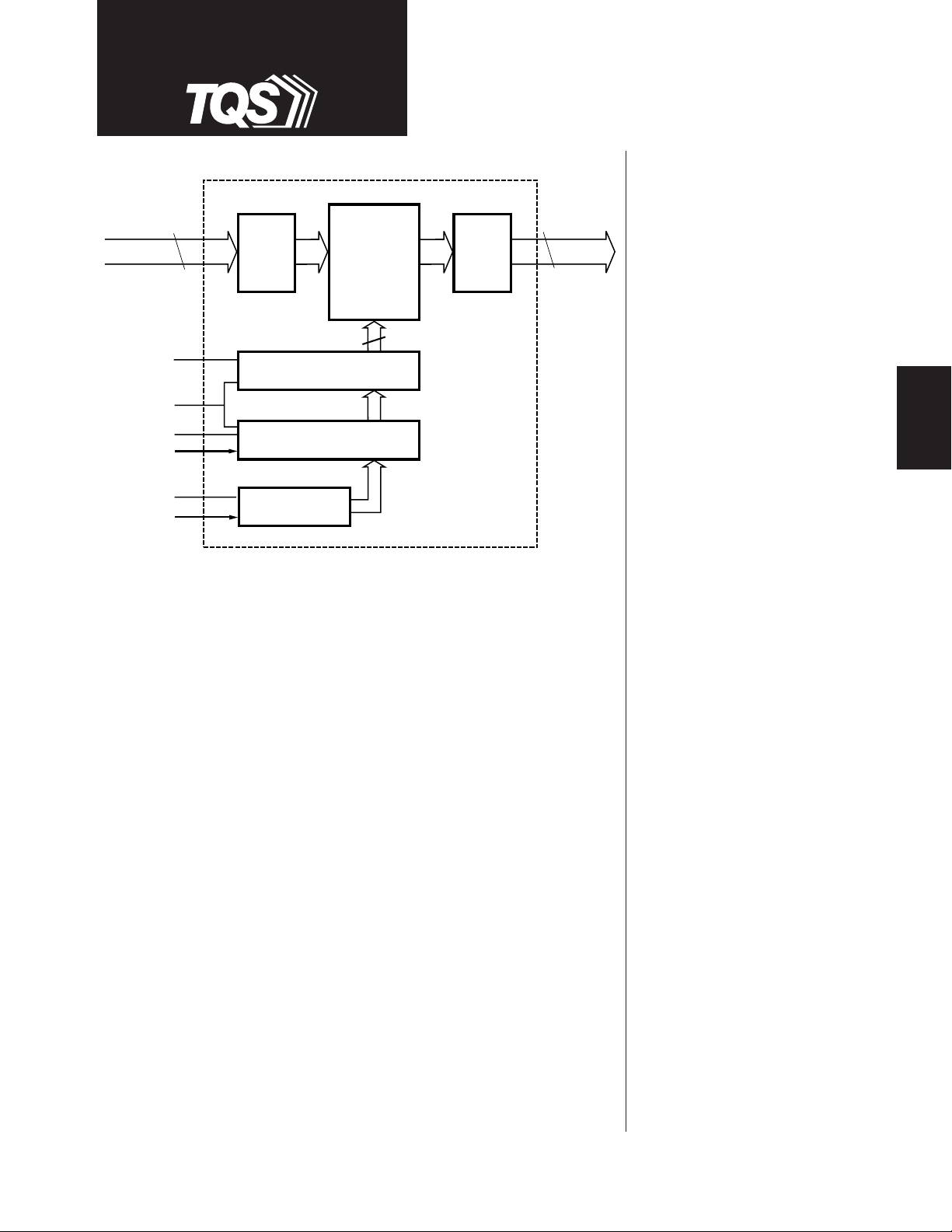
64 x 33
Crosspoint
Switch Matrix
Output
Buffers
TQ8033
O0–O32
66
D0–D63
CONFIGURE
RESETIN
LOAD
IADD(0:5)
MONITOR_LD
O
ADD(0:4)
Input
Buffers
128
33 6-Bit Configuration Latches
33 6-Bit Program Latches
5:32 Decoder
The TQ8033 is a non-blocking 64 x 33 digital crosspoint switch that
supports data rates greater than 1.5 gigabits per second per channel.
The TQ8033's non-blocking architecture allows any combination of
output-to-input programming, supporting both broadcast and multicast
applications. Using 33 independent 64:1 multiplexers, each output
channel can be programmed to any input without restriction or
degradation of signal fidelity.
1.5 Gbit/sec
64x33 Expandable
Crosspoint Switch
Features
• >1.5 Gb/s/port data rate
>50 Gb/s aggregate bandwidth
• Differential PECL data path with
64 inputs and 33 outputs
• Non-blocking architecture
supports Broadcast and
Multicast operation
• Data inputs internally biased for
AC coupling
• Low jitter and signal skew
• Double-buffered configuration
latches
• TTL configuration control inputs
PRODUCTS
SWITCHING
The TQ8033's architecture is ideally suited for building larger switch
arrays. By eliminating the need to "wire-or" or buss the outputs to
interconnect multiple devices, the maximum system bandwidth and signal
fidelity is achived.
Designed for use in high-performance / high-capacity switching
applications, the TQ8033 data path is fully differential to minimize jitter,
skew, and signal distortion. The data path interface levels are PECL and
the configuration and control interface levels are TTL.
The TQ8033 is the ideal switching solution for HDTV digital video, data
communications (Fibre Channel and Gigabit Ethernet) and
telecommunications applications.
For additional information and latest specifications, see our website: www.triquint.com
• 304-pin BGA package
• Single +5V supply
Applications
• Telecom/datacom switching
including Fibre Channel and
Gigabit Ethernet
• Hubs and routers
• Video switching including
High-Definition TV (HDTV)
1
Page 2

TQ8033
DATA SHEET
Circuit Description
Data Inputs
The 64 data input channels are differential PECL
compatible. All inputs have a 2.5KΩ Thevenin
equivalent bias circuit which holds the DC bias at
-1.3 Volts simplifying the design of applications
V
DD
requiring AC coupling. Input signals must be properly
terminated for maximum performance. Terminate one
side (true or complement) of any unused inputs to V
Data Outputs
The 33 data output channels are differential PECL
compatible and designed to be terminated to 50Ω to
-2.0 Volts. Unused outputs can be left
V
DD
unterminated if desired in order to save power.
Control Inputs
To program the TQ8033, the address of the desired
output port is applied to the inputs (OADD0:4; where
00000=O0 and 11111=O31). The address of the desired
input port is applied to the inputs (IADD0:5; where
000000=I0 and 111111=I63).
The new configuration is loaded into the program
registers by asserting the LOAD signal high. The data
is latched when LOAD is de-asserted. LOAD should
.
remain low and only be asserted for the time necessary
TT
to load the new configuration data.
The process is repeated for each output port
configuration. Only the output ports which are to
receive a new input port configuration need to be
programmed. The new configurations are not applied
to the switch core at this time and there is no
disruption of the data flowing through the switch core.
The control inputs interface levels are TTL compatible.
Program Registers
The configuration data for each of the 33 data channels
have two sets, or stages, of configuration storage
registers. The first stage, known as the program
register, stores a new set of input configurations prior
to application to the switch core. The second stage,
known as the configuration register, stores the current
switch core configurations.
The use of two stage configuration storage registers
allows new input configurations to be loaded without
disturbing the existing configuration. After the new
input configurations have been loaded into the program
registers, the CONFIGURE input is asserted and the
new configurations are applied to the switch core.
After the new configurations have been loaded into the
program registers, the CONFIGURE input is asserted
and the data in the program registers is loaded into the
configuration registers. The data is latched on the
falling edge of CONFIGURE.
The switch core receives the new configuration as soon
as CONFIGURE is asserted. During the time the new
configurations are being applied to the switch core, the
integrity of the data on output ports which receive a
tdcf
new configuration is unknown for a period of
from
the time CONFIGURE is asserted.
If desired, the LOAD and CONFIGURE can be asserted
simultaneously. In this mode, the new configuration
will be applied to the switch core when LOAD is
asserted.
2
For additional information and latest specifications, see our website: www.triquint.com
Page 3

TQ8033
DATA SHEET
Programming the Monitor Port
The 33rd output port, called the monitor port, is
programmed in the same manner as the other 32
output ports with the exceptions that the LOAD and
Output Address inputs are ignored.
To program the monitor port, apply the desired input
port address to inputs (IADD0:5) and assert the
MONITOR_LD input. Like the other 32 output ports, the
CONFIGURE input is asserted to apply the new
configuration to the switch core.
Reset Programming
The RESETIN is an active high input which sets all of
the switch multiplexers to a defined configuration.
There are three RESET modes available when RESETIN
is used in conjunction with CONFIGURE and IADD5
inputs.
The monitor port is reset to input D0 regardless of the
state of CONFIGURE or IADD5.
Mode 1 is broadcast operation. In this mode, the
RESETIN signal clears all of the configuration registers
immediately forcing all output ports to be connected to
input port 0. The device will remain in the Mode 1 reset
state as long as the RESETIN input is asserted.
Modes 2 and 3 place the device into pass-through
configuration. The mode is controlled by the assertion
of CONFIGURE immediately following the de-assertion
of RESETIN and the state of input IADD5.
Mode 2, or low-order pass-through, is set with the
assertion of CONFIGURE with IADD5 input low. In this
mode, inputs D0 to D31 are configured to outputs O0
to O31 respectively (D0 to O0, D1 to O1,,,D31 to O31).
Mode 3, or high-order pass-through, is set with the
assertion of CONFIGURE with IADD5 input high. In this
mode, inputs D32 to D63 are configured to outputs O0
to O31 respectively (D32 to O0, D33 to O1,,,D63 to
O31).
PRODUCTS
SWITCHING
Reset Configuration Modes
Mode RESETIN CONFIGURE** IADD5** RESET Configuration
1 1 0 X Broadcast mode. All outputs programmed to input 0
2 1 1 0 Low-order Pass-through mode #1.
3 1 1 1 High-order Pass-through mode #2.
** Valid only when asserted immediately following de-assertion of RESETIN and prior to any new program cycles.
For additional information and latest specifications, see our website: www.triquint.com
3
Page 4
TQ8033
DATA SHEET
Building Switch Arrays with the TQ8033
By eliminating the need to “wire-or” the outputs of
multiple devices or to add additional switch elements to
get the necessary routing channels, the TQ8033 offers
the highest performance solution with the least number
of devices for implementing larger array sizes.
The 33rd output port provides an additional data
channel for system data links or for diagnostics system
monitoring of each switch element within the array. The
following examples show how to interconnect multiple
TQ8033 devices to create a 64x64 and a 128x128
switch array.
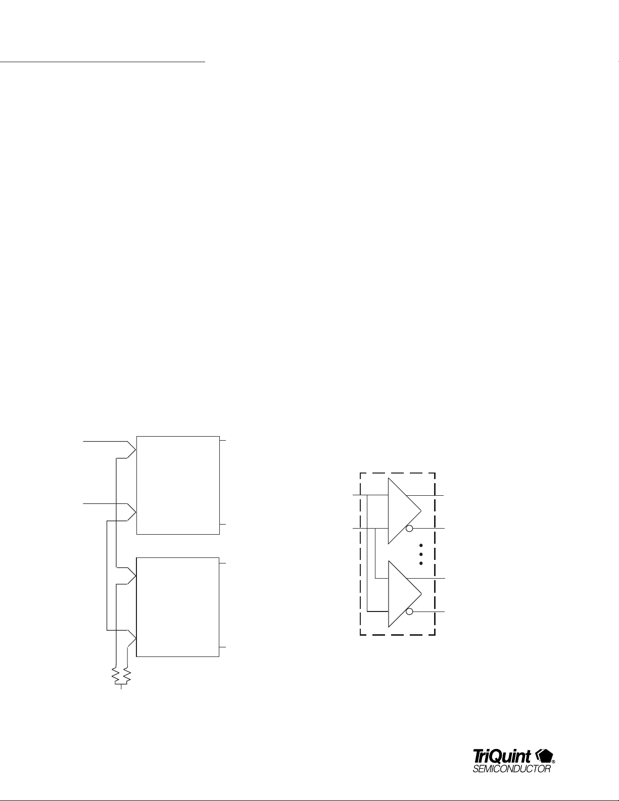
64x64 Switch Array
To implement a 64x64 array
(figure 2)
, only two
TQ8033 devices are required and the data passes
through only one switch element. For applications with
data rates less than one gigabit per second, a technique
known as"fly-by" termination offers good signal fidelity
with the minimum number of components. To
implemement, both the input signal pairs (true and
complement) are routed to both devices and then to the
termination network at the end of the signal trace with
the minimum number of trace discontinuities.
To accomplish this, route the trace from the source
device to the first TQ8033 input pad and then continue
the signal trace from the input pads to the next device,
and finally to the termination network.
For applications at data rates above one gigabit per
second, it is recommended to use a fan-out buffer to
drive each TQ8033 input as shown in
figure 3
.
As with any high speed interconnect, careful attention
to the impedance of the signal traces is very important.
D0
O0
TQ8033
D63
O31
O32
TQ8033
O63
50
50
Ω
V
Figure 2. 64x64 array with "fly-by" termination
Ω
TT
Dn/
NDn
Connect one driver
output to each
common TQ8033
input
Figure 3. Optional fan-out buffer for array expansion
4
For additional information and latest specifications, see our website: www.triquint.com
Page 5
TQ8033
DATA SHEET
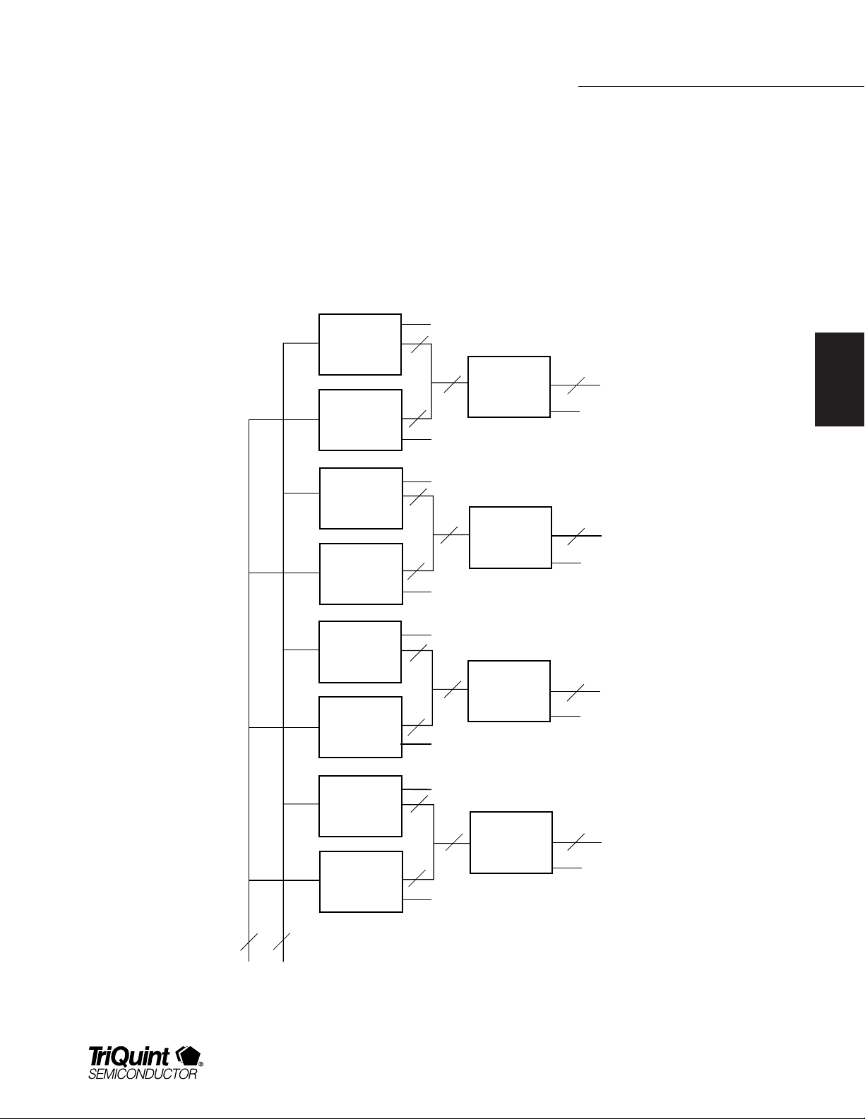
128x128 Switch Array
To implement a 128x128 switch array, simply extend
the design of the 64x64 switch array to include the
additional devices. In this configuration, only 12
TQ8033 devices are required and the signal passes
through only two switch stages.
TQ8033
64x33
Crosspoint
Switch
TQ8033
64x33
Crosspoint
Switch
TQ8033
64x33
Crosspoint
Switch
TQ8033
64x33
Crosspoint
Switch
Monitor
Monitor
Monitor
Monitor
Again, use “fly-by” interconnection or a fan-out buffer on
input signals to connect multiple devices and the far-end
termination network.
Larger switch arrays can be built by simply adding
additional TQ8033 devices.
32
64
32
32
64
32
TQ8033
64x33
Crosspoint
Switch
TQ8033
64x33
Crosspoint
Switch
32
Monitor
32
Monitor
D0-31
D32-63
PRODUCTS
SWITCHING
D0-63
6464
D64-127
TQ8033
64x33
Crosspoint
Switch
TQ8033
64x33
Crosspoint
Switch
TQ8033
64x33
Crosspoint
Switch
TQ8033
64x33
Crosspoint
Switch
Monitor
32
32
Monitor
Monitor
32
32
Monitor
64
64
Figure 4. 128x128 array
TQ8033
64x33
Crosspoint
Switch
TQ8033
64x33
Crosspoint
Switch
32
D64-95
Monitor
32
D96-127
Monitor
For additional information and latest specifications, see our website: www.triquint.com
5
Page 6
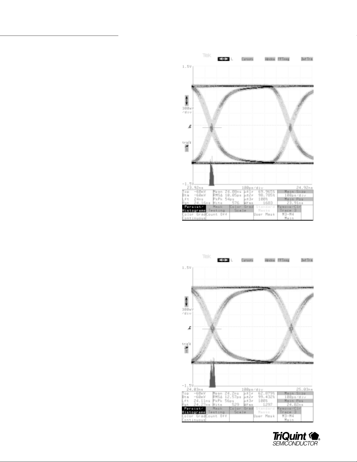
Typical Performance
Data Rate: 1.5Gb/s
Data Pattern: 2
Case Temperature: 0° C
Jitter: 54 ps pk-pk
TQ8033
DATA SHEET
23-1
PRBS
Data Rate: 1.5Gb/s
23-1
Data Pattern: 2
PRBS
Case Temperature: 85° C
Jitter: 56 ps pk-pk
6
For additional information and latest specifications, see our website: www.triquint.com
Page 7

Typical Performance
Crosspint Devices: 2 (Cascaded)
Data Rate: 1.5Gb/s
Data Pattern: 2
Case Temperature: 85° C
Jitter: 110 ps pk-pk
23-1
PRBS
TQ8033
DATA SHEET
PRODUCTS
SWITCHING
Rise and Fall Time
Data Rate: 1.5Gb/s
Data Pattern: 2
Case Temperature: 85° C
Rise/Fall time: 170/166 ps
23-1
PRBS
For additional information and latest specifications, see our website: www.triquint.com
7
Page 8

TQ8033
DATA SHEET
Specifications
Specifications subject to change without notice
Table 1. DC Characteristics — PECL I/O
3,4
Parameter Notes/Condition Symbol Minimum Nominal Maximum Unit
Input common mode range V
Differential pk-pk input voltage swing (1, 2) ∆V
Differential pk-pk output voltage swing (1, 2) ∆V
Output common mode range V
Input capacitance C
ESD breakdown rating V
Table 2. DC Characteristics—TTL I/O
3
ICOM
IN
OUT
OCOM
IN
ESD
VDD – 1500 — VDD – 1100 mV
800 — 2400 mV
1200 2200 mV
VDD-1500 VDD-1100 mV
— 2.6 3.3 pF
1000 — — V
Parameter Notes/Condition Symbol Minimum Nominal Maximum Unit
Input HIGH voltage V
Input LOW voltage V
Input HIGH current V
Input LOW current V
IH(MAX)
IL(MIN)
Input capacitance C
ESD breakdown rating V
I
IH
I
IL
ESD
IH
IL
IN
2.0 — V
DD
0 — 0.8 V
— — 200 uA
–400 –200 — uA
— — 3.3 pF
1000 — — V
V
Notes (Tables 1 and 2):
1. Defined as
2. R
LOAD
3. Specifications apply over recommended operating ranges.
4. Inputs are internally DC-biased to V
(2 x (| V
= 50 ohms to VTT = VDD – 2.0V.
TRUE
- V
COMP
|))
– 1.3V with 2.5KΩ Thevenin input impedance for applicaitons requiring AC coupling.
DD
8
For additional information and latest specifications, see our website: www.triquint.com
Page 9

TQ8033
DATA SHEET
Table 3. AC Characteristics
Parameter Notes/Condition Symbol Minimum Nominal Maximum Unit
Maximum Data Rate/port 1.5 Gb/s
D0-63 minimum pulse width (1) T
O0-32 Rise/Fall time 20-80% (1) T
Channel Propagation Delay (mean) (1) T
Ch-to-Ch Propagation Delay Skew (1) T
O0-32 Jitter (2) T
pw
r/f
pd
skew
jitter
500 — — ps
— — 250 ps
— — 2.5 ns
200 500 ps
— 85 200 ps
Notes: 1. Min. VOH to max VOL levels
2. Crossing of (On) – (NOn) measured with 2
Figure 5. Timing Diagram
Input Address
[IADD5:0]
Output Address
[OADD4:0]
LOAD
CONFIGURE
D (63:0)
O (32:0)
23
– 1 PRBS, measured over extended time.
Valid Address
Valid Address
tsar[IADD]
tsar[OADD]
tpd
Tpwl
Tldh
thar
Tpwc
Tdcf
Data Not Valid **
tldl
Data Valid
PRODUCTS
SWITCHING
** Data valid on outputs with unchanged configurations
Table 4. Timing Specifications
Symbol Parameter Minimum Maximum Unit
t
sar[OADD]
t
sar[IADD]
t
har
t
pwl
t
ldh
t
pwc
t
dcf
t
ldl
Output Address to Load Set-up time 1 ns
Input Address to Load Set-up time 1 ns
Address to Load Hold Time 2.5 ns
Min. Load pulse width 2.5 ns
Load to Configure delay 0 ns
Min. Configure pulse width 7 ns
Configure to Data Valid 15 ns
Configure to Load delay 3 ns
For additional information and latest specifications, see our website: www.triquint.com
9
Page 10

TQ8033
DATA SHEET
Table 5. Absolute Maximum Ratings
4
Parameter Condition Symbol Minimum Nominal Maximum Unit
Storage Temperature T
Junction Temperature T
Case Temperature w/bias (1) T
Supply Voltage (2) V
Voltage to any input (2) V
Voltage to any output (2) V
Current to any input (2) I
Current from any output (2) I
Power Dissipation of output (3) P
Notes: 1. Tc is measured at case top.
2. All voltages are measured with respect to GND (0V) and are continuous.
3. Pout = (V
4. Absolute maximum ratings, as detailed in this table, are the ratings beyond which the device’s performance may be impaired
and/or permanent damage to the device may occur.
DD
– V
out
) x I
out
.
store
CH
C
DD
in
out
in
out
out
–65 150 °C
–65 150 °C
0 100 °C
0 7.0 V
–0.5 VDD + 0.5 V
–0.5 V
+ 0.5 V
DD
–1.0 1.0 mA
40.0 mA
50.0 mW
Table 6. Recommended Operating Conditions
4
Symbol Parameter Min Typ Max Units Notes
T
C
V
DD
I
DD
V
TT
R
LOAD
Θ
JC
Notes: 1. TC measured at case top. Use of adequate heatsink is required.
Case Operating Temperature 0 — 85 °C 1, 3
Supply Voltage 4.75 — 5.25 V
Current Positive Supply 3 A
Load Termination Supply Voltage VDD – 2.0 V 2
Output Termination Load Resistance 50 Ω 2
Thermal Resistance Junction to Case 2.2 °C/W
2. The V
3. Contact the Factory for extended temperature range applications.
4. Functionality and/or adherence to electrical specifications is not implied when the device is subjected to conditions that exceed,
and R
TT
singularly or in combination, the operating range specified.
combination is subject to maximum output current and power restrictions.
LOAD
10
For additional information and latest specifications, see our website: www.triquint.com
Page 11

Figure 6. Typical high speed measurement
TQ8033
V
DD
TQ8033
DATA SHEET
OUT
PECL
V
DD
NOUT
PECL
PECL/ECL
Termination
PECL/ECL
Termination
OUT
VBias
NOUT
Scope
50
Ω
GND
50
Ω
GND
** PECL/ECL terminations available from
Cascade Microtech model 523-0150 and
OUT - NOUT
PRODUCTS
SWITCHING
Picosecond Pulse Labs model 5623
For additional information and latest specifications, see our website: www.triquint.com
11
Page 12

TQ8033
DATA SHEET
Figure 7. Pinout —Bottom View
2322212019
151413
18
17
16
304-pin BGA
bottom view
12
TQ8033
11
10
1
9
8
432
7
6
5
A
B
C
D
E
F
G
H
J
K
L
M
N
P
R
T
U
V
W
Y
AA
AB
AC
GND
VDD
Table 7. Pin Descriptions
Signal Type Grid Ref. Description
Not Connected B7, C1, C8, T3, U2, AA16, AB17 - DO NOT CONNECT - LEAVE OPEN
VDD A1, A23, B2, B22, C3, C5, C19, C21, D3, D4, D6, D9, D12, D15, D18, D20, D21, F4, F20
J4, J20, M4, M20, R4, R20, V4, V20, W3, W21, Y4, Y6, Y9, Y12, Y15, Y18, Y20, AA3,
AA5, AA19, AA21, AB2, AB22, AC1, AC23
GND A2, A6, A8, A9, A12, A15, A16, A18, A22, B1, B3, B21, B23, C2, C22, F1, F23, H1, H23,
J1, J23, M1, M23, R1, R23, T1, T23, V1, V23, AA2, AA22, AB1, AB3, AB21, AB23, AC2,
AC6, AC8, AC9, AC12, AC15, AC16, AC18, AC22
RESETIN TTL Input E20 Active high. Reset loads program registers with default input.
LOAD TTL Input C23 Active high, Loads input port data into the selected output port's
program registers. Output port definfed by OADD(0:4)
CONFIGURE TTL Input D22 Active high. Transfers the data for all program registers into the
second stage configure registers and into the switch core.
MONITOR_LD TTL Input E4 Active High. Directly loads the 33rd output port program register. The
OADD(0:5) and LOAD are not used to program this port.
IADD0 TTL Input E21 Input address LSB. (D0= 000000, D63= 111111)
IADD1 TTL Input D23 Input address.
IADD2 TTL Input E22 Input address.
IADD3 TTL Input F21 Input address.
IADD4 TTL Input G20 Input address.
IADD5 TTL Input E23 Input address MSB.
(Continued on next page)
12
For additional information and latest specifications, see our website: www.triquint.com
Page 13

TQ8033
DATA SHEET
Table 7. Pin Descriptions (cont.)
Signal Type Grid Ref. Description
OADD0 TTL Input F22 Output address LSB. (O0=00000, O31= 11111)
OADD1 TTL Input G21 Output address.
OADD2 TTL Input H20 Output address.
OADD3 TTL Input G22 Output address.
OADD4 TTL Input H21 Output address MSB.
Data Inputs
D0, ND0 PECL Input C20, D19 High-speed input and complement.
D1, ND1 PECL Input A21, B20 High-speed input and complement.
D2, ND2 PECL Input A20, B19 High-speed input and complement.
D3, ND3 PECL Input C18, D17 High-speed input and complement.
D4, ND4 PECL Input A19, B18 High-speed input and complement.
D5, ND5 PECL Input C17, D16 High-speed input and complement.
D6, ND6 PECL Input B17, A17 High-speed input and complement.
D7, ND7 PECL Input C16, B16 High-speed input and complement.
D8, ND8 PECL Input C15, B15 High-speed input and complement.
D9, ND9 PECL Input D14, C14 High-speed input and complement.
D10, ND10 PECL Input B14, A14 High-speed input and complement.
D11, ND11 PECL Input D13, C13 High-speed input and complement.
D12, ND12 PECL Input B13, A13 High-speed input and complement.
D13, ND13 PECL Input C12, B12 High-speed input and complement.
D14, ND14 PECL Input A11, B11 High-speed input and complement.
D15, ND15 PECL Input C11, D11 High-speed input and complement.
D16, ND16 PECL Input A10, B10 High-speed input and complement.
D17, ND17 PECL Input C10, D10 High-speed input and complement.
D18, ND18 PECL Input B9, C9 High-speed input and complement.
D19, ND19 PECL Input B8, A7 High-speed input and complement.
D20, ND20 PECL Input D8, C7 High-speed input and complement.
D21, ND21 PECL Input B6, A5 High-speed input and complement.
D22, ND22 PECL Input D7, C6 High-speed input and complement.
D23, ND23 PECL Input B5, A4 High-speed input and complement.
D24, ND24 PECL Input B4, A3 High-speed input and complement.
D25, ND25 PECL Input D5, C4 High-speed input and complement.
D26, ND26 PECL Input D2, E3 High-speed input and complement.
D27, ND27 PECL Input D1, E2 High-speed input and complement.
D28, ND28 PECL Input F3, G4 High-speed input and complement.
D29, ND29 PECL Input E1, F2 High-speed input and complement.
D30, ND30 PECL Input G3, H4 High-speed input and complement.
D31, ND31 PECL Input G2, G1 High-speed input and complement.
PRODUCTS
SWITCHING
(Continued on next page)
For additional information and latest specifications, see our website: www.triquint.com
13
Page 14

TQ8033
DATA SHEET
Table 7. Pin Descriptions (cont.)
Signal Type Grid Ref. Description
Data Inputs (cont.)
D32, ND32 PECL Input W2, Y1 High-speed input and complement.
D33, ND33 PECL Input Y2, AA1 High-speed input and complement.
D34, ND34 PECL Input W4, Y3 High-speed input and complement.
D35, ND35 PECL Input AA4, Y5 High-speed input and complement.
D36, ND36 PECL Input AC3, AB4 High-speed input and complement.
D37, ND37 PECL Input AC4, AB5 High-speed input and complement.
D38, ND38 PECL Input AA6, Y7 High-speed input and complement.
D39, ND39 PECL Input AC5, AB6 High-speed input and complement.
D40, ND40 PECL Input AA7, Y8 High-speed input and complement.
D41, ND41 PECL Input AB7, AC7 High-speed input and complement.
D42, ND42 PECL Input AA8, AB8 High-speed input and complement.
D43, ND43 PECL Input AA9, AB9 High-speed input and complement.
D44, ND44 PECL Input Y10, AA10 High-speed input and complement.
D45, ND45 PECL Input AB10, AC10 High-speed input and complement.
D46, ND46 PECL Input Y11, AA11 High-speed input and complement.
D47, ND47 PECL Input AB11, AC11 High-speed input and complement.
D48, ND48 PECL Input AA12, AB12 High-speed input and complement.
D49, ND49 PECL Input AC13, AB13 High-speed input and complement.
D50, ND50 PECL Input AA13, Y13 High-speed input and complement.
D51, ND51 PECL Input AC14, AB14 High-speed input and complement.
D52, ND52 PECL Input AA14, Y14 High-speed input and complement.
D53, ND53 PECL Input AB15, AA15 High-speed input and complement.
D54, ND54 PECL Input AB16, AC17 High-speed input and complement.
D55, ND55 PECL Input Y16, AA17 High-speed input and complement.
D56, ND56 PECL Input AB18, AC19 High-speed input and complement.
D57, ND57 PECL Input Y17, AA18 High-speed input and complement.
D58, ND58 PECL Input AB19, AC20 High-speed input and complement.
D59, ND59 PECL Input AB20, AC21 High-speed input and complement.
D60, ND60 PECL Input Y19, AA20 High-speed input and complement.
D61, ND61 PECL Input Y21, W20 High-speed input and complement.
D62, ND62 PECL Input AA23, Y22 High-speed input and complement.
D63, ND63 PECL Input Y23, W22 High-speed input and complement.
(Continued on next page)
14
For additional information and latest specifications, see our website: www.triquint.com
Page 15

TQ8033
DATA SHEET
Table 7. Pin Descriptions (cont.)
Signal Type Grid Ref. Description
Data Outputs
O0,NO0 PECL Output H3,H2 High-speed output and complement.
O0 and NO0 are addressed by OADD = “00000”.
O31 and NO31 are addressed by OADD = “11111”.
O1, NO1 PECL Output J3, J2 High-speed output and complement.
O2, NO2 PECL Output K4, K3 High-speed output and complement.
O3, NO3 PECL Output K2, K1 High-speed output and complement.
O4, NO4 PECL Output L4, L3 High-speed output and complement.
O5, NO5 PECL Output L2, L1 High-speed output and complement.
O6, N06 PECL Output M3, M2 High-speed output and complement.
O7, NO7 PECL Output N1, N2 High-speed output and complement.
O8, NO8 PECL Output N3, N4 High-speed output and complement.
O9, NO9 PECL Output P1, P2 High-speed output and complement.
O10, NO10 PECL Output P3, P4 High-speed output and complement.
O11, NO11 PECL Output R2, R3 High-speed output and complement.
O12, NO12 PECL Output T2, U1 High-speed output and complement.
O13, NO13 PECL Output T4, U3 High-speed output and complement.
O14, NO14 PECL Output V2, W1 High-speed output and complement.
O15, NO14 PECL Output U4, V3 High-speed output and complement.
O16, NO16 PECL Output J22, J21 High-speed output and complement.
O17, NO17 PECL Output K21, K20 High-speed output and complement.
O18, NO18 PECL Output K23, K22 High-speed output and complement.
O19, NO19 PECL Output L21, L20 High-speed output and complement.
O20, NO20 PECL Output L23, L22 High-speed output and complement.
O21, NO21 PECL Output M21, M22 High-speed output and complement.
O22, NO22 PECL Output N22, N23 High-speed output and complement.
O23, NO23 PECL Output N20, N21 High-speed output and complement.
O24, NO24 PECL Output P22, P23 High-speed output and complement.
O25, NO25 PECL Output P20, P21 High-speed output and complement.
O26, NO26 PECL Output R21, R22 High-speed output and complement.
O27, NO27 PECL Output T21, T22 High-speed output and complement.
O28, NO28 PECL Output U22, U23 High-speed output and complement.
O29, NO29 PECL Output U21, T20 High-speed output and complement.
O30, NO30 PECL Output W23, V22 High-speed output and complement.
O31, NO31 PECL Output V21, U20 High-speed output and complement.
O32, NO32 PECL Output H22, G23 High-speed monitor output and complement.
PRODUCTS
SWITCHING
For additional information and latest specifications, see our website: www.triquint.com
15
Page 16

TQ8033
DATA SHEET
Figure 8. Pin assignment - Top view
AA
AB
AC
A
B
C
D
E
F
G
H
J
K
L
M
N
P
R
T
U
V
W
Y
1
VCC
GND
D27
D29
GND
ND31
GND
GND
NO3
NO5
GND
GND
GND
NO12
GND
NO14
ND32
ND33
GND
VCC
1
O7
O9
=
NC
3
2
GND
ND24
VCC
GND
VCC
GND
D26
VCC VCC
ND27
ND26
ND29
D28
D31
D30
NO0
O0
O1
NO1
O3
NO2
NO4
O5
O6
NO6
O8
NO7
NO9
O10
NO11
O11
O12
NO13
O14
NO15
VCC
D32
ND34
D33
GND
VCC
GND
D36
3
2
(Not Connected)
4
ND23
D24
ND25
MONITOR_LD
VCC
ND28
ND30
VCC
O2
O4
VCC
NO8
NO10
VCC
O13
O15
VCC
D34
D35
ND36
D37
4
5
6
ND21
GND
D21
D23
ND22
VCC
D25
VCC VCC
VCCVCC
ND35
VCCVCC
D38
ND37
ND39
D39
GNDGND
5
6
ND19
ND20
ND38
ND41
7
D22
9
8
10
D16
GND
GND
D18
ND18
ND16
D17
ND17
D19
D20
12
11
D14
GND GND
ND14
ND13
D15
D13
VCC
ND15
TQ8033
304-pin SBGA
Top View
VCCVCC
D46
ND40
D40
D42
D41
ND42
GND
7
8
D44
=
D43
ND43
9
DNC
ND46
D47
ND47
11
D48
ND48
GNDGND
12
ND44
D45
ND45
10
(DO NOT CONNECT. LEAVE OPEN)
14
13
ND12
ND11
ND50
ND49
D49
13
15
16
17
18
ND10
D12
D10
ND9
D9
D11 ND5 ND0
ND52
D52
D50
ND51
D51
14
GND
ND8
ND7
D8
D7
VCC VCC
VCC
D55
ND53
D53
D54
GNDGND
15
16
ND6
ND3
D57
ND55
ND54
17
GND
D6
ND4
D5
ND57
D56
GND
18
19
ND2
VCC
D60
D58
ND56
19
D4
20
D2
ND1
D0D3
VCC VCC
RESETIN
VCC
IADD4
OADD2
VCC
NO17
NO19
VCC
O23
O25
VCC
NO29
NO31
VCC
ND61
VCCVCC
ND60
D59
ND58
20
21
DNC
IADD0
IADD3
OADD1
OADD4
NO16
NO25
21
D1
GND
O17
O19
O21
NO23
O26
O27
O29
O31
VCC
D61
VCCVCC
GND
ND59
22
GND
VCC
GND
CONFIG
IADD2
OADD0
OADD3
O32
O16
NO18
NO20
NO21
O22
O24
NO26
NO27
O28
NO30
ND63
ND62
GND
VCC
GND
22
23
VCC
GND
LOAD
IADD1
IADD5
GND
NO32
GND
GND
O18
O20
GND
NO22
NO24
GND
GND
NO28
GND
O30
D63
D62
GND
VCC
23
A
B
C
D
E
F
G
H
J
K
L
M
N
P
R
T
U
V
W
Y
AA
AB
AC
16
For additional information and latest specifications, see our website: www.triquint.com
Page 17

Figure 9. SBGA Mechanical Dimensions
TQ8033
DATA SHEET
PRODUCTS
SWITCHING
Table 8. SBGA Dimensions (in millimeters)
Symbol Parameter Min. Nom. Max.
A Overall thickness — — 1.70
A
1
A
2
D Body size — 31.00 —
D
1
E Body size — 31.00 —
E
1
M,N Ball Matrix 23 x 23
M1 Number of Rows 4
b Ball diameter 0.60 0.75 0.90
d Distance encapsulation to balls 0.5 — —
e Ball pitch 1.27
ddd Coplanarity 0.15 0.30 0.35
ccc Encapsulation height — — 0.20
T Metal back thickness 0.050 0.125 0.175
S Solder ball placement — 0.00 —
Ball Height 0.50 0.60 0.70
Body thickness 0.85 0.91 1.00
Ball footprint 27.84 27.94 28.04
Ball footprint 27.84 27.94 28.04
PCB pad size — 0.63 —
For additional information and latest specifications, see our website: www.triquint.com
17
Page 18

TQ8033
DATA SHEET
Thermal Management
Most applications will require the use of a heatsink or
other thermal management system in order to keep the
package case temperature within the recommended
operation limits. As long as the package case
temperature does not exceed 85 degrees C, the die
temperature will remain well within TriQuint’s
requirements for reliability.
Selection of a thermal management device is very
dependent on the system mechanical and
environmental constrains. Several vendors of heatsink
and other thermal management systems support the
TQ8033’s thermally enhanced Ball Grid Array package.
These vendors will work with you to evaluate the
system requirements and recommend the best
solution.
Heat Sink Vendors
Aavid Thermal Technologies
One Kool Path
P.O. Box 400
Laconia, NH 03247
603-528-3400
Sumitomo Metal (SMI)
2953 Bunker Hill Lane
Santa Clara, CA 95054
408-982-0990
Wakefield Engineering, Inc.
60 Audubon Road
Wakefield, MA 01880
617-345-5900
Ordering Information
TQ8033 1.5 Gbit/sec 64x33 Crosspoint Switch
Additional Information
For latest specifications, additional product information, worldwide sales and distribution locations, and
information about TriQuint:
Web: www.triquint.com Tel: (503) 615-9000
Email: sales@tqs.com Fax: (503) 615-8900
For technical questions and additional information on specific applications:
Email: applications@tqs.com
The information provided herein is believed to be reliable; TriQuint assumes no liability for inaccuracies or omissions. TriQuint assumes no
responsibility for the use of this information, and all such information shall be entirely at the user's own risk. Prices and specifications are subject
to change without notice. No patent rights or licenses to any of the circuits described herein are implied or granted to any third party.
TriQuint does not authorize or warrant any TriQuint product for use in life-support devices and/or systems.
Copyright © 1998 TriQuint Semiconductor, Inc. All rights reserved.
Revision 1.0.A November 1999
18
For additional information and latest specifications, see our website: www.triquint.com
 Loading...