

Page 1
T R I Q U I N T S E M I C O N D U C T O R , I N C .
TQ8025
PRELIMINARY DATA SHEET
2.5 Gigabit/sec
DIØ–15
(differential)
32
PECL/CML
Input
Buffers
16 x 16
Crosspoint
Switch Matrix
PECL/CML
Output
Buffers
32
DOØ–15
(differential)
Configuration
Latches
4-Bit Shift
Register
4-Bit Shift
Register
16 x 4
Address Generator
and Control
READY
+5V
GND
RADDØ
RADD1
RESET–
LDMODE
CONFIG
ADD15
ADDØ
LOAD
CLOCK
ADDREN
AUTOCONFIG
TQ8025
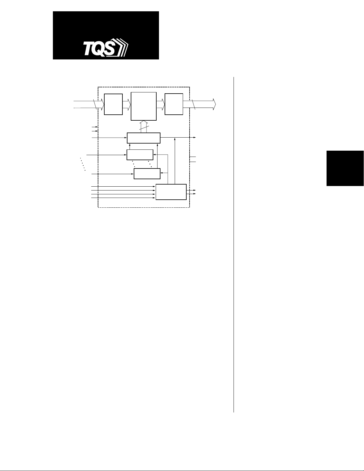
The TQ8025 is a non-blocking 16 x 16 digital crosspoint switch capable of
data rates greater than 2.5 gigabits per second per port. With a fully
differential internal data path and PECL/CML I/O, the TQ8025 offers an
extremely high data rate with exceptional signal fidelity. The use of fully
differential logic results in low crosstalk, jitter, and signal skew. The
TQ8025 is ideally suited for digital video, data communications,
telecommunication switching, and cross-connect applications.
The non-blocking architecture uses 16 fully independent 16:1 multiplexers
which allow each output port to be independently programmed to any input
port. The TQ8025 offers two programming options: a flexible port-by-port
option, and a fast configuration option.
16x16 Digital
Crosspoint Switch
Features
• 16 PECL/CML fully differential
(back-terminated) outputs
• >2.5 Gb/s data bandwidth
per channel
• >40 Gb/s aggregate bandwidth
• Non-blocking architecture
• 80 ns configuration time
• Autonomous control of external
RAM for configuration data
• Low jitter and signal skew
•
±
100 ps delay match (one input
to all outputs)
• Fully differential data path
• 132-pin MLC package with
heat spreader
PRODUCTS
SWITCHING
Using the fast configuration option, all 16 switch ports are programmed
within 80ns by serially loading four 16-bit input port selection words. Two
output pins (RADD0,1) are provided to drive an external RAM
(n x 4 x 16 bits) used to store the switch configuration. An Autoconfigure
option automatically transfers the new configurations into the switch core.
Autoconfiguration occurs after the last input selection word is clocked into
the programming registers.
Data integrity is maintained on all unchanged data paths for both the portby-port and fast configuration options.
For additional information and latest specifications, see our website: www.triquint.com
Applications
• SONET OC-48 data path
• Double-speed Fibre Channel
• Hubs and routers
• High-definition video switching
• Parallel processing
1
Page 2

PRELIMINARY DATA SHEET
Specifications
TQ8025
Table 1. Absolute Maximum Ratings
Storage temperature
Junction temperature
Case temperature with bias
Supply voltage
2
Voltage to any input
Voltage to any output
Current to any input
Current from any output
Power dissipation of output
1
2
2
2
2
3
4
T
T
T
V
V
V
I
I
P
IN
OUT
STORE
CH
C
CC
IN
OUT
OUT
–65 °C to +150 °C
150 °C
T
= 150 °C
J
0 V to +7.0 V
–0.5 V to VCC + 0.5 V
–0.5 V to VCC + 0.5 V
–1.0 mA to +1.0 mA
40 mA
50 mW
Notes: 1. TC is measured at the case top.
2. All voltages are measeured with respect to GND 0V and are continuous.
3. P
= (VCC – V
OUT
OUT
) x I
OUT
.
4. Absolute maximum ratings in this table are those beyond which the device's performance may be impaired
and/or permanent damage may occur.
Table 2. Recommended Operating Conditions
4
Symbol Parameter Min Typ Max Units Notes
T
C
V
CC
V
TT
I
CC
R
LOAD
Θ
JC
Notes: 1. TC measured at case top. Use of adequate heatsink is required.
Case Operating Temperature 0 — 85 °C 1, 3
Supply Voltage 4.75 — 5.25 V
Load Termination Supply Voltage V
Current Positive Supply — — 2.1 A
Output Termination Load Resistance 50 Ω 2
Thermal Resistance Channel to Case 4.5 °C/W
2. The V
and R
TT
combination is subject to maximum output current and power restrictions.
LOAD
– 2.0 V 2
CC
3. Contact the Factory for extended temperature range applications.
4. Functionality and/or adherence to electrical specifications is not implied when
the device is subjected to conditions that exceed, singularly or
in combination, the operating range specified.
2
For additional information and latest specifications, see our website: www.triquint.com
Page 3

TQ8025
PRELIMINARY DATA SHEET
Table 3. DC Characteristics — CML I/O
5
Symbol Description Test Conditions Min Nom Max Unit
V
COM
V
DIFF
V
IH
V
IL
V
OH
V
OL
I
OH
I
OL
Table 4. DC Characteristics — PECL I/O
Common mode voltage (Note 1) VCC – 600 — V
CC
Differential voltage (Note 1) 400 — 1200 mV
Input HIGH voltage (Note 2) — V
CC
Input LOW voltage VCC – 1100 — mV
Output HIGH voltage (Note 3) VCC – 100 — V
CC
Output LOW voltage (Note 3) VCC – 1100 — VCC – 600 mV
Output HIGH current (Note 3, 4) 20 23 30 mA
Output LOW current (Note 3, 4) 0 5 8 mA
5
Symbol Description Test Conditions Min Nom Max Unit
V
V
V
V
V
V
I
I
C
C
COM
DIFF
IH
IL
OH
OL
OH
OL
IN
OUT
Common mode voltage (Note 1) VCC – 1500 — VCC – 1100 mV
Differential voltage (Note 1) 400 — 1200 mV
Input HIGH voltage (Note 2) — VCC – 500 mV
Input LOW voltage VCC – 2100 — mV
Output HIGH voltage (Note 3) VCC – 1100 — V
– 600 mV
CC
Output LOW voltage (Note 3) VCC – 2100 — VCC – 1600 mV
Output HIGH current (Note 4) 20 23 30 mA
Output LOW current (Note 4) 0 5 8 mA
Input capacitance — — TBD pF
Output capacitance — — TBD pF
VESD ESD breakdown rating (Note 5) Class I — —
mV
mV
mV
PRODUCTS
SWITCHING
Table 5. DC Characteristics — TTL I/O
5
Symbol Description Test Conditions Min Nom Max Unit
V
IH
V
IL
I
IH
I
IL
V
OH
V
OL
C
IN
C
OUT
Input HIGH voltage 2.0 — V
CC
Input LOW voltage 0 — 0.8 V
Input HIGH current V
Input LOW current V
(IHMAX)
(ILMIN)
Output HIGH voltage IOH = 50 mA 2.4 — V
— — 200 uA
–400 –200 — uA
CC
Output LOW voltage IOH = –20 mA 0 — 0.4 V
Input capacitance — — TBD pF
Output capacitance — — TBD pF
VESD ESD breakdown rating (Note 5) Class I — —
Notes (Tables 3, 4, and 5): 1. Differential inputs.
= 1300 mV.
2. V
REF
= 50 ohms to VTT = VCC – 2.0 V.
3. R
LOAD
4. Not tested; consistent with V
5. Specifications apply over recommended operating ranges.
For additional information and latest specifications, see our website: www.triquint.com
and VOL tests.
OH
V
V
3
Page 4

TQ8025
PRELIMINARY DATA SHEET
Table 6. AC Characteristics
Symbol Description Test Conditions Min Typ Max Unit
T
PW
T
R/F
T
PD
T
SKEW
T
JITTER
D(0:15) minimum pulse width (Note 1) 360 — — ps
O(0:15) rise/fall time 20-80% (Note 1) — — 150 ps
D(0:15), O(0:15) delay time (Note 1) — — 2.5 ns
Path delay matching (Note 1) 300 ps
Jitter (Note 2) — 50 — ps pk–pk
Notes: 1. Minimum V
2. Crossing of (On)—(NOn) measured with 2
Table 7. TQ8025 Timing — Normal Configure Mode
to maximum VOL levels.
OH
23
– 1 PRBS, measured over extended time.
1
Symbol Parameter Min. Max. Units
T1 Hold LOAD low to SAD0:3, DAD0:3 2 ns
T2 Setup DAD0:3 to LOAD high 0 ns
T3 CONFIGURE pulse low time 10 ns
T4 Setup LOAD low to CONFIGURE low 3 ns
T5 CONFIGURE low to SIGNAL PATHS updated 4 ns
T6 LOAD pulse width high TBD ns
Notes: 1. LDMODE = 0; AUTOCONFIG = Don't Care, RESET– = 1, CLOCK = Don't Care.
Figure 1. TQ8025 Timing —␣ Normal Configure Mode
DAD0:3
SAD0:3
LOAD
CONFIGURE
DEST ADDR 1 DEST ADDR 2
T1 T1
SRCE ADDR 1 SRCE ADDR 2
T6
T2
T4 T3
SIGNAL PATHS
LDMODE=0; AUTOCONFIG = Don't Care, RESET– = 1, CLOCK = Don't Care.
4
For additional information and latest specifications, see our website: www.triquint.com
OLD CONFIGURATION
T5
NEW CONFIGURATION
Page 5

TQ8025
PRELIMINARY DATA SHEET
Table 8. TQ8025 Timing — RAM Loading, Auto-Configure Mode
1
Symbol Parameter Min. Max. Units
T1 LOAD high to READY low 3 ns
T2 CLOCK low to READY high 3 ns
T3 ADDREN low to RADD enabled 3 ns
T4 Setup LOAD high to CLOCK high 4 ns
T5 CLOCK low to RADD increment 2 ns
T6 AD0:15 setup before CLOCK low 0 ns
T7 AD0:15 hold time after CLOCK low 2 ns
T8 CLOCK low to INT CONFIGURE high 2 ns
T9 CONFIGURE low pulse width 10 ns
T10 ADDREN high to RADD tristate 3 ns
T11 LOAD low prior to 3rd CLOCK low 4 ns
T12 LOAD high pulse TBD ns
T13 CLOCK low to SIGNAL PATHS updated 4 ns
T14 CLOCK period 20 ns
T15 LOAD high to INT CONFIGURE low TBD ns
Notes: 1. LDMODE = 1; AUTOCONFIG = 1, RESET– = 1, CONFIG = 1.
Figure 2. TQ8025 Timing —␣ RAM Loading, Auto-Configure Mode
PRODUCTS
SWITCHING
CLOCK
T4
LOAD
ADDREN
RADD0:1
READY
AD0:15
INT CONFIGURE
SIGNAL PATHS
LDMODE = 1; AUTOCONFIG = 0, RESET– = 1.
T12 T11
T3
0123 0
T1
T6 T7
D0 D1 D2 D3
T15
T5
OLD CONFIGURATION NEW CONFIGURATION
T14
Note: INT CONFIGURE is an internal signal shown for clarity of operation.
For additional information and latest specifications, see our website: www.triquint.com
T8
T13
T10
T2
T9
T1
T15
5
Page 6

TQ8025
PRELIMINARY DATA SHEET
Table 9. TQ8025 Timing — RAM Loading, External Configure Pulse Mode
1
Symbol Parameter Min. Max. Units
T1 LOAD high to READY low 3 ns
T2 CLOCK low to READY high 3 ns
T3 ADDREN low to RADD enabled 3 ns
T4 Setup LOAD high to CLOCK high 4 ns
T5 CLOCK low to RADD increment 2 ns
T6 AD0:15 setup before CLOCK low 0 ns
T7 AD0:15 hold time after CLOCK low 2 ns
T8 Setup last CLOCK before CONFIGURE low 2 ns
T9 CONFIGURE low pulse width 10 ns
T10 ADDREN high to RADD tristate 3 ns
T11 LOAD low prior to 3rd CLOCK low 4 ns
T12 LOAD high pulse TBD ns
T13 CONFIGURE low to READY low TBD ns
T14 CONFIGURE low to SIGNAL PATHS updated 4 ns
T15 CLOCK period 20 ns
Notes: 1. LDMODE = 1; AUTOCONFIG = 0, RESET– = 1.
Figure 3. TQ8025 Timing —␣ RAM Loading, External Configure Pulse Mode
CLOCK
T4
T12
LOAD
ADDREN
RADD0:1
READY
AD0:15
CONFIGURE
SIGNAL PATHS
LDMODE = 1; AUTOCONFIG = 1, RESET– = 1, CONFIG = 1.
6
T3 T5
0123 0
T1 T2
T6 T7
D0
For additional information and latest specifications, see our website: www.triquint.com
T15
T11
D1 D2 D3
OLD CONFIGURATION
T10
T13
T8
T9
T14
NEW CONFIGURATION
Page 7

Typical Performance
Data Rate: 2.5Gb/s
Data Pattern: 2^7 PRBS
Note: Measured jitter is 68ps pk-pk.
Signal source jitter is 32ps pk-pk.
TQ8025
PRELIMINARY DATA SHEET
PRODUCTS
SWITCHING
Rise and Fall
Data Rate: 2.5Gb/s
Rise Time: 115ps
Fall Time: 109ps
For additional information and latest specifications, see our website: www.triquint.com
7
Page 8

TQ8025
PRELIMINARY DATA SHEET
Figure 4. TQ8025 pinout — top view
N.C.
N.C.
Vcc
Vcc
32 31 30 29 2827 26 25 2423 22 21 20 19 1817 16 15 14 1312 11 10 9 8 7 6 5 4 3 2 1
33
GND
Vcc
AD15
AD14
AD13
AD12
Vcc
AD11
AD10
AD09
AD08
Vcc
AD07/DAD3
AD06/DAD2
AD05/DAD1
AD04/DAD0
Vcc
AD03/SAD3
AD02/SAD2
AD01/SAD1
AD00/SAD0
Vcc
RADD0
RADD1
LOAD
RESET-
AUTOCONFIG
Vcc
CLOCK
CONFIG
READY-
Vcc
Vcc
34
35
36
37
38
39
40
41
42
43
44
45
46
47
48
49
50
51
52
53
54
55
56
57
58
59
60
61
62
63
64
65
66
67 68 69 70 7172 73 74 75 76 7778 79 80 81 8283 84 85 86 8788 89 90 91 9293 94 95 9697 98 99
TT
TT
DI08N
DI08P
Vcc
V
V
DI09N
DI09P
Vcc
DI10N
DI10P
TQ8025
132-pin Heat Spreader
Cavity Down
Top View
DI11N
DI11P
Vcc
DI12N
DI12P
DI13N
DI13P
Vcc
DI14N
DI14P
DI15N
DI15P
DO15N
Vcc
DO15P
DO14N
Vcc
DO14P
GND
132
131
130
129
128
127
126
125
124
123
122
121
120
119
118
117
116
115
114
113
112
111
110
109
108
107
106
105
104
103
102
101
100
Vcc
Vcc
DO13N
DO13P
DO12N
DO12P
Vcc
DO11N
DO11P
DO10N
DO10P
Vcc
DO09N
DO09P
DO08N
DO08P
Vcc
DO07N
DO07P
DO06N
DO06P
Vcc
DO05N
DO05P
DO04N
DO04P
Vcc
DO03N
DO03P
DO02N
DO02P
Vcc
GND
TT
TT
V
V
Vcc
GND
8
For additional information and latest specifications, see our website: www.triquint.com
ADDREN
LDMODE
Vcc
DI00P
DI00N
DI01P
DI01N
Vcc
DI02P
DI02N
DI03P
DI03N
Vcc
DI04P
DI04N
DI05P
DI05N
Vcc
DI06P
DI06N
DI07P
DI07N
Vcc
DO00P
DO00N
DO01P
DO01N
Vcc
Vcc
Page 9

TQ8025
PRELIMINARY DATA SHEET
Table 10. TQ8025 Pin Descriptions
Signal Name/Level Description
DI00P-DI15P Data input true and complement Differential data input ports. VH = 0 V, VL = –300 mV max.
DI0N-DI15N Differential CML/PECL input
DO0P-DO15P, Data output true and complement Differential data output ports. 600 mV min. differential swing.
DO0N-DO15N Differential CML/PECL output
AD00:15 Input address; TTL input
RADD0:1 RAM address; TTL output, tristate Used to generate address 0-3 during configure load from RAM.
ADDREN Enable RADD0:2; TTL input
CLOCK Clock; TTL input Controls cycle time of address generator and AUTOCONFIG.
AUTOCONFIG Configure mode; TTL input When high, internal CONFIGURE is automatically generated.
READY READY; open-drain output
LOAD LOAD; TTL input
CONFIGURE CONFIGURE; TTL input Used to load address contents of internal address registers.
LDMODE Load Mode; TTL input When floated high, AD0-15 are used for configuration.
SAD0:3 Source Address; TTL inputs When LDMODE is low, specifies input address to be connected
DAD0:3 Destination Address; TTL input
VCC, GND, VTT +5V, Ground; Power and ground pins.
Termination Voltage VTT = GND for CML inputs; VTT = VCC – 2V for PECL inputs.
RESET– Reset; TTL Input
Internal 50-ohm terminations to VTT (CML = 0 V;ECL = –2.0 V).
Serial input address, LSB first in time; ADn programs output port n.
When low, enables RADD0:1; when high, forces RADD0:1 tristate.
Indicates end of AUTOCONFIG or
when high. Reset low by RESET-, CONFIG low, or LOAD rising.
Requires external pullup to VCC.
For LDMODE=1, ADDREN=0: AUTOCONFIG=0, rising LOAD causes
ADDR0:1 to generate RAM addresses, then READY is asserted
after four clock ticks. For AUTOCONFIG=1, LOAD rising causes
ADDR0:1 to generate addresses, causing an internal CONFIG
to be generated, after which READY is asserted.
s
ee SAD0:3 and DAD0:3
Active LOW. Crosspoint will be configured within 4 ns
(objective) of CONFIG falling low.
When tied low, SAD0-3 and DAD0-3 are used for configuration.
When AUTOCONFIG is disabled, and AD08-15 are ignored.
to output port specified by DAD0:3. Latched by falling LOAD
(LDMODE=0).
When LDMODE is low, specifies output address to be connected
to input port specified by SAD0:3. Latched by falling LOAD
(LDMODE=0).
While low, programs all output ports to connect to input port 0.
Strobing CONFIG after reset restores user port programming
if device power was stable since last user programming and
during RESET–. Active low, Schmitt triggered.
end of address LOAD cycle
For LDMODE=0,
.
PRODUCTS
SWITCHING
For additional information and latest specifications, see our website: www.triquint.com
9
Page 10

TQ8025
PRELIMINARY DATA SHEET
Figure 5. Mechanical Dimensions
132
1.170 +.006
.950 +.006
.800
Top viewBottom view
PIN 1
INDEX
1
Section A-A
.060
SEATING PLANE
Ordering Information
TQ8025
Additional Information
CERAMIC OR
METAL LID
CHIP CAPACITOR, 4 PLACES
HEAT SPREADER
DEVICE
.125
.064
A
.025
1. Part is symmetrical about the center axes.
2. Centerline bisects center pin in both directions.
3. See pad detail below.
0.025
centers
C
L
0.525
C
L
2.5 Gb/s 16x16 Crosspoint Switch
0.325
± .005
.010 +.0015
BSC
0.105
PAD LAYOUT DETAIL
A
0.015
0.010
For latest specifications, additional product information,
worldwide sales and distribution locations, and information about TriQuint:
Web: www.triquint.com Tel: (503) 615-9000
Email: sales@tqs.com Fax: (503) 615-8900
For technical questions and additional information on specific applications:
Email: applications@tqs.com
The information provided herein is believed to be reliable; TriQuint assumes no liability for inaccuracies or
ommisions. TriQuint assumes no responsibility for the use of this information, and all such information
shall be entirely at the user's own risk. Prices and specifications are subject to change without notice.
No patent rights or licenses to any of the circuits described herein are implied or granted to any third party.
TriQuint does not authorize or warrant any TriQuint product for use in life-support devices and/or systems.
Copyright © 1998 TriQuint Semiconductor, Inc. All rights reserved.
Revision 0.3.A August 1998
10
For additional information and latest specifications, see our website: www.triquint.com
 Loading...