

Page 1
T R I Q U I N T S E M I C O N D U C T O R , I N C .
SWITCHING
PRODUCTS
1
For additional information and latest specifications, see our website: www.triquint.com
TQ8017
Min Max Units
Data Rate/port 1.25 Gb/s
Jitter 150 ps pk-pk
Channel Propagation Delay 2000 ps
Ch-to-Ch Propagation Delay Skew 500 ps
Typical output waveform with
all channels driven
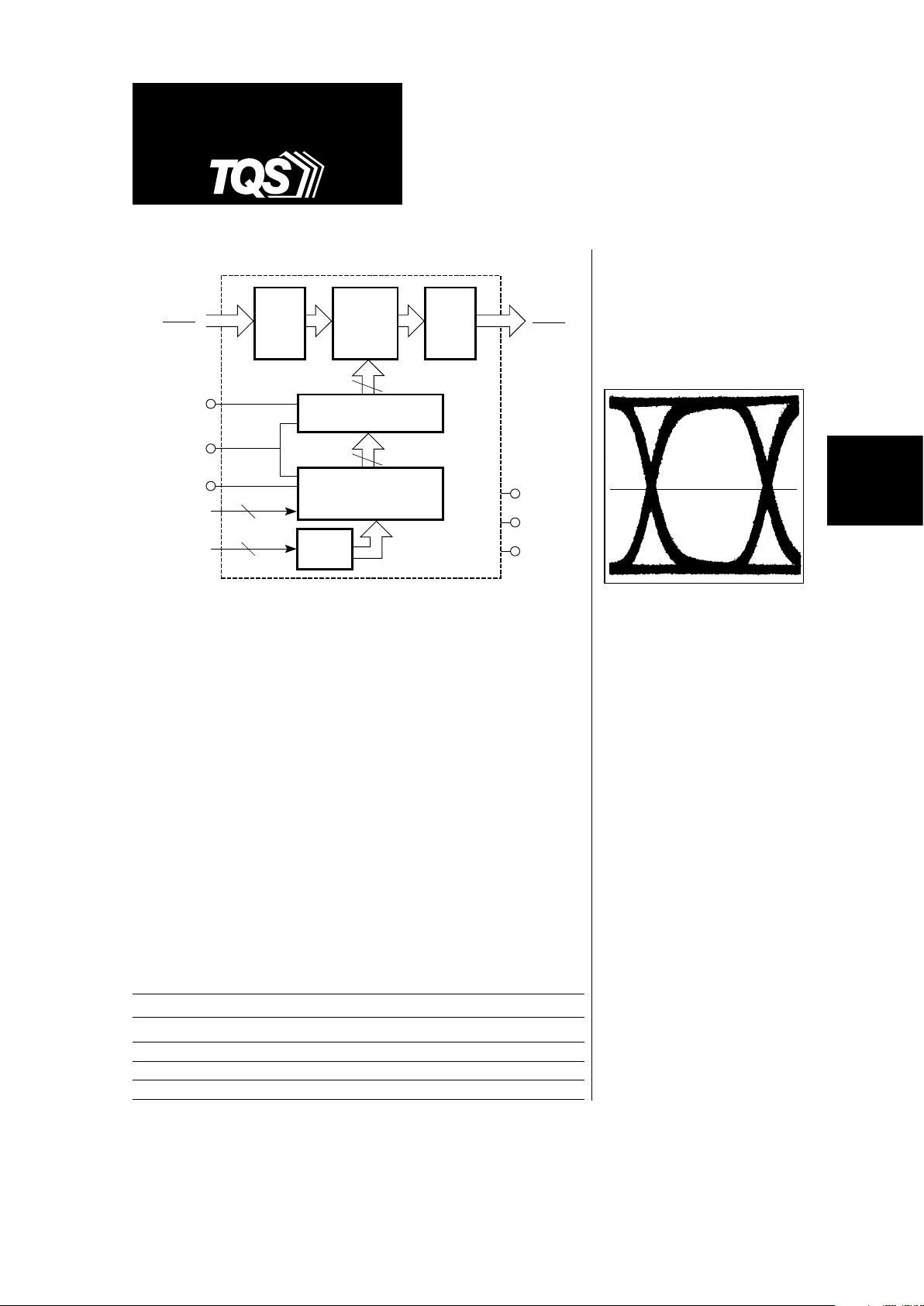
The TQ8017 is a non-blocking 16 x 16 digital crosspoint switch capable of
data rates greater than 1.25 Gigabits per second per port. Utilizing a fully
differential internal data path and PECL I/O, the TQ8017 offers a high data
rate with exceptional signal fidelity. The symmetrical switching and noise
rejection characteristics inherent in differential logic result in low jitter and
signal skew. The TQ8017 is ideally suited for digital video, data
communications and telecommunication switching applications.
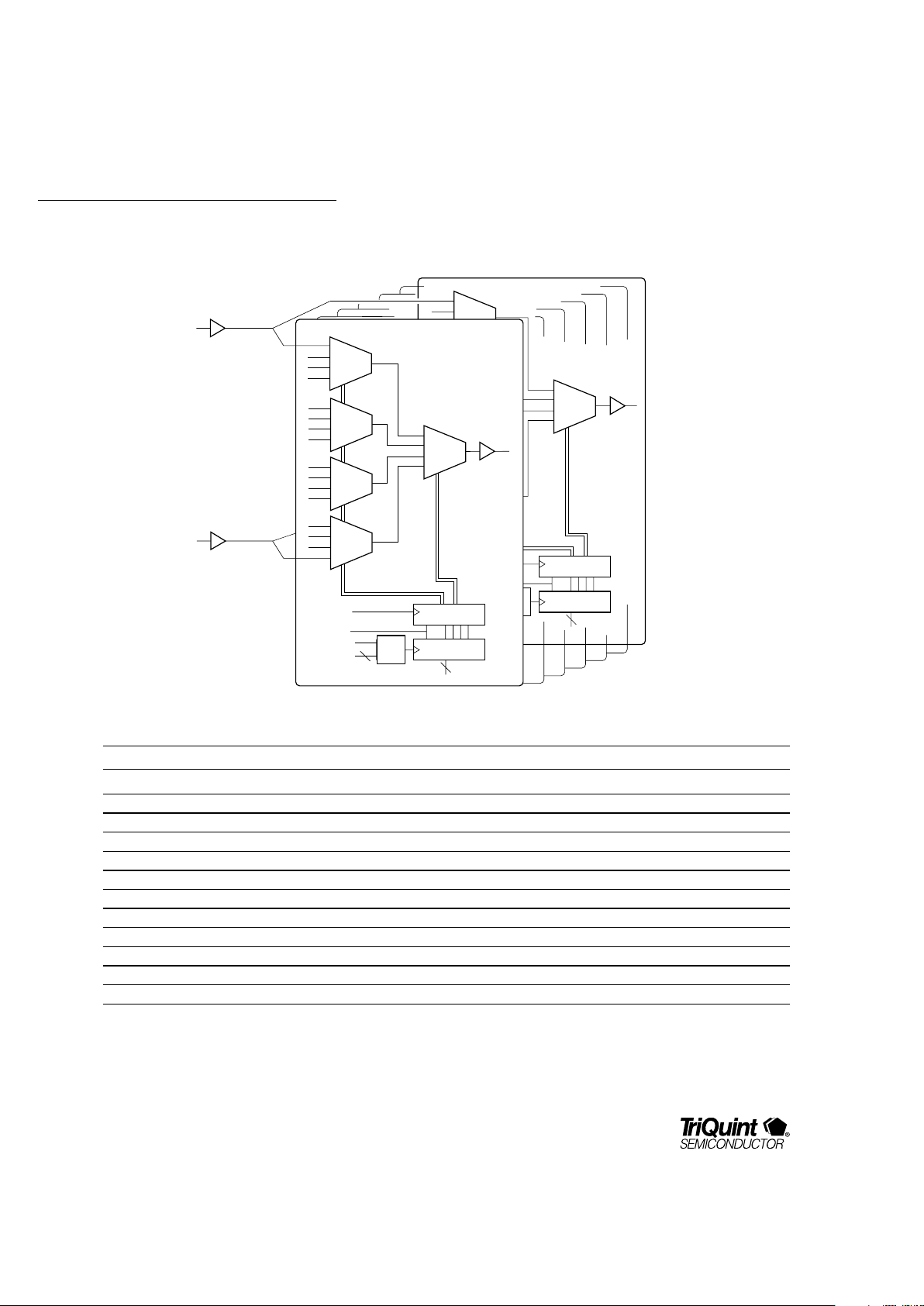
The non-blocking architecture uses 16 fully independent 16:1 multiplexers
(see diagram on page 2), allowing each output port to be independently
programmed to any input port. The switch is configured by sequentially
loading each multiplexer’s 4-bit program latch (OA0:3) with the desired
input port address (IA0:3) and enabling the LOAD pin. When complete, the
CONFIGURE pin is strobed and all new configurations are simultaneously
transferred into the switch multiplexers. Data integrity is maintained on all
unchanged data paths.
Applications
• Telecom/Datacom Switching
• Hubs and Routers
• Video Switching
• >20 Gb/s aggregate BW
• 1.25 Gb/s/port NRZ data rate
• Non-blocking architecture
• 500 ps delay match
• Differential PECL-level data
I/O; Selectable CMOS/TTLlevel control inputs
• Low jitter and signal skew
• Fully differential data path
• Double-buffered
configuration latches
• 132-pin MQFP package
• Single +5V supply
Electrical Characteristics
Features
1.25 Gigabit/sec
16x16 Digital PECL
Crosspoint Switch
Input
Buffers
Output
Buffers
16 x 16
Crosspoint
Switch
Matrix
64
64
(R2)
Sixteen 4-Bit Latches
(R1)
Sixteen 4-Bit Addressable
Output Select Latches
4
4
4:16
Decoder
VCC
VEE
GND
O0..15
O0..15
D0..15
D0..15
CONFIGURE
RESET
LOAD
IA0..3
OA0..3
TQ8017
Page 2
TQ8017
For additional information and latest specifications, see our website: www.triquint.com
2
Symbol Parameter Absolute Max. Rating Notes
T
STOR
Storage Temperature –65° C to +150° C
T
CH
Junction (Channel) Temperature –65° C to +150° C1
T
C
Case Temperature Under Bias –65° C to +125° C2
V
CC
Supply Voltage 0 V to +7 V 3
V
TT
Load Termination Supply Voltage VCC to 0 V 4
V
IN
Voltage Applied to Any PECL Input; Continuous GND –0.5 V to VCC +0.5 V
I
IN
Current Into Any PECL Input; Continuous –1.0 mA to +1.0 mA
V
IN
Voltage Applied to Any TTL/CMOS Input; Continuous –0.5 V to VCC +0.5 V
I
IN
Current Into Any TTL/CMOS Input; Continuous –1.0 mA to +1.0 mA
V
OUT
Voltage Applied to Any PECL Output GND –0.5 V to VCC +0.5 V 4
I
OUT
Current From Any PECL Output; Continuous –40 mA
P
D
Power Dissipation per Output P
OUT
= (GND – V
OUT
) x I
OUT
50 mW
Notes: 1. For die applications.
2. T
C
is measured at case top.
3. All voltages specified with respect to GND, defined as 0V.
4. Subject to I
OUT
and power dissipation limitations.
5. Absolute maximum ratings, as detailed in this table, are the ratings beyond which the device's performance may be impaired
and/or permanent damage to the device may occur.
Figure 1. TQ8017 Architecture
Table 1. Absolute Maximum Ratings
5
DATA
OUT 15
(O15)
5
RESET
OUTPUT
SELECT ADDRESS
(OA0:3)
Input
Buffers
DATA
OUT 0
(O0)
Configuration
Register
Program Register
CONFIGURE
LOAD
4
16 X 1-BIT
MULTIPLEXER
16 X 1-BIT
MULTIPLEXER
.
.
.
.
.
.
.
.
.
.
.
.
DATA IN 0
(D0)
DATA IN 15
(D15)
4
INPUT ADDRESS
(IA0:3)
4:16
DECODE
Page 3
TQ8017
SWITCHING
PRODUCTS
3
For additional information and latest specifications, see our website: www.triquint.com
Symbol Parameter Min Typ Max Units Notes
T
C
Case Operating Temperature 0 85 °C 1,3
V
CC
Supply Voltage 4.5 5.5 V
V
TT
Load Termination Supply Voltage V
CC
– 2.0 V 2
R
LOAD
Output Termination Load Resistance 50 Ω 2
Θ
JC
Thermal Resistance Junction to Case 7 °C/W
Notes: 1. TC measured at case top. Use of adequate heatsink is required.
2. The V
TT
and R
LOAD
combination is subject to maximum output current and power restrictions.
3. Contact the Factory for extended temperature range applications.
4. Functionality and/or adherence to electrical specifications is not implied when the device is subjected to conditions that exceed,
singularly or in combination, the operating range specified.
Table 2. Recommended Operating Conditions
4
Table 3. Pin Descriptions
Signal Name/Level Description
D0 to D15, Data input true and complement. Differential data input ports.
ND0 to ND15 Differential PECL
O0 to O15, Data output true and complement. Differential data output ports.
NO0 to NO15 Differential PECL
IA0:3 Input address. CMOS/TTL Input port selection address that is written into the selected output port
program latches (OA0:3).
IA3 IA2 IA1 IA0 Input port
0000 0
0001 1
0010 2
:::: :
1111 15
OA0:3 Output select address. Output port selection address. Selects the output port program latches to
CMOS/TTL which the input port selection address (IA0:3) is written.
OA3 OA2 OA1 OA0 Output port
0000 0
0001 1
0010 2
:::: :
1111 15
LOAD CMOS/TTL Enables the selected output port program latches while set ‘high’.
Latches the data when set to a 'low' level.
CONFIGURE CMOS/TTL Transfers the program latches data to the configuration latches and
implements the switch changes while set ‘high’. Latches the data when
set to a ‘low’ level.
RESET CMOS/TTL Configures the switch into Broadcast or Pass-Through mode, overwriting
existing configurations.
Broadcast mode:
All output ports are connected to data input port 0. This
mode is selected by applying a RESET “high” pulse with CONFIGURE held “low."
Pass-through mode: I0 is connected to O0, I1 to O1, etc. This mode is
selected by applying a RESET “high” pulse with CONFIGURE held “high."
CNTRL LVL Input level control. GND/Open Selects the input levels for the input address (IA0:3), output address
(OA0:3), CONFIGURE, LOAD and RESET inputs. Inputs are configured
for TTL when tied to GND and CMOS when left unconnected.
Page 4

TQ8017
For additional information and latest specifications, see our website: www.triquint.com
4
Symbol Parameter Min Max Units Test Cond. Notes
V
IH
PECL Input Voltage High V
CC
–1.1 V
CC
– 0.5 V
V
IL
PECL Input Voltage Low V
TT
V
CC
– 1.5 V
I
IH
PECL Input Current High +30 µ A VIH = V
CC
– 0.7 V
I
IL
PECL Input Current Low –30 µA VIL = V
CC
– 2.0 V
V
ICM
PECL Input Common Mode Voltage V
CC
– 1.5 V
CC
–1.1 V
V
IDIF
PECL Input Differential Voltage (pk-pk) 400 1200 mV
V
IH
CMOS/TTL Input Voltage High 3.5/2.0 VCC/V
CC
V2
V
IL
CMOS/TTL Input Voltage Low 0/0 1.5/0.8 V 2
I
IH
CMOS/TTL Input Current High +200 µAV
IH
= V
CC
2
I
IL
CMOS/TTL Input Current Low –100 µAV
IL
= 0 V 2
V
OCM
PECL Output Common Mode V
CC
– 1.5 V
CC
–1.1 V
V
ODIF
PECL Output Differential Voltage 600 mV
V
OH
PECL Output Voltage High V
CC
–1.0 V
CC
– 0.6 V
V
OL
PECL Output Voltage Low V
TT
V
CC
– 1.6 V
I
OH
PECL Output Current High 20 27 mA
I
OL
PECL Output Current Low 0 8 mA
I
CC
Power Supply Current (+) 970 mA
Table 4. DC Characteristics
1,2
– Within recommended operating conditions, unless otherwise indicated.
Notes: 1. Test conditions unless otherwise indicated: VTT = VCC – 2.0 V, R
LOAD
= 50 Ω to V
TT.
2. Input level is selected by the CNTRL LVL input. Tying CNTRL LVL to GND selects TTL levels, leaving CNTRL LVL OPEN selects
CMOS levels.
Table 5. AC Characteristics1 – Within recommended operating conditions, unless otherwise indicated.
Symbol Parameter Min Typ Max Units Notes
Maximum Data Rate/Port 1.25 Gb/s 1,2
Jitter 150 ps pk-pk 1
T
1
Channel Propagation Delay 2000 ps 3
T
2
Ch-to-Ch Propagation Delay Skew 500 ps
T
3
CONFIG to Data Out (Oi) Delay 5 ns
T
4
LOAD Pulse Width 7 ns
T
5
CONFIG Pulse Width 7 ns
T
6
IAi to LOAD High Setup Time 0 ns
T
7
LOAD to IAi Low Hold Time 3 ns
T
8
OAi to LOAD High Setup Time 0 ns
T
9
LOAD to OAi Low Hold Time 3 ns
T
10
Load ↑ to CONFIG ↑ 0ns
T
11
RESET Pulse Width 10 ns
T
R,F
Output Rise or Fall Time 250 400 ps 3
Notes: 1. Test conditions: V
CC
= 5.0 V; V
TT
= 3.0 V, R
LOAD
= 50 Ω to VTT; PECL inputs: VIH = 3.9 V; VIL = 3.5 V; CMOS inputs: VIH = 3.5 V,
V
IL
= 1.5 V; PECL outputs: VOH > 4.0 V, VOL < 3.4 V; PECL inputs rise and fall times < 1 ns; CMOS inputs rise and fall times
< 20 ns. A bit error rate of 1E–13 BER or better for 223–1PRBS pattern, jitter and rise/fall times are guaranteed through characterization.
2. 1.2 Gb/s Non-Return-Zero (NRZ) data equivalent to 600 MHz clock signal.
3. Rise and fall times are measured at the 20% and 80% points of the transition from V
OL
max to VOL min.
Page 5

TQ8017
SWITCHING
PRODUCTS
5
For additional information and latest specifications, see our website: www.triquint.com
Figure 2. Timing Diagram – Switch Configuration
Output
Address
Input
Address
LOAD
RESET
CONFIGURE
A
D
B
D
C
D
D
D
E
D
F
D
G
D
A
O
B
O
C
O
D
O
E
O
F
O
G
O
T8 T7
T5
T6
T1
T9
T3
Invalid
Data Out
T10
T4
Data
1
In
Data
1
Out
Notes: 1. No data loss on unchanged paths
Figure 3. Timing Diagram – Reset
Output
Data
RESET
CONFIGURE
T11
T3
Broadcast Pass-through
Notes: 1. LOAD input must remain LOW to insure correct programming of the switch.
2. “Broadcast” is defined as data input 0 to all data outputs (0…15).
3. “Pass-through” is defined as data input 0 to data output 0, data input 1 to data output 1, etc.
Page 6

TQ8017
For additional information and latest specifications, see our website: www.triquint.com
6
Typical Performance Data
0.5 0.7 0.9 1.1 1.3 1.5 1.7
12
10
8
6
4
2
0
Data Rate (Gb/s)
Data Eye Period (%)
Figure 4. Data Eye Closure
0.5 0.7 0.9 1.1 1.3 1.5 1.7
55
50
45
40
35
30
25
20
15
10
Data Rate (Gb/s)
Jitter (ps)
Figure 6. RMS Jitter vs. Data Rate (typical)
0.5 0.7 0.9 1.1 1.3 1.5 1.7
100
90
80
70
60
50
40
30
20
10
0
Data Rate (Gb/s)
Percent (%)
➤
% Recoverable Data Eye
Period – (P-P Jitter) x 100 / Period
➤
Inner Eye Amplitude
V (inner eye) x 100 / V (inner eye @ 400 Mb/s)
Figure 5. Data Eye Closure
Time & Amplitude vs Data Rate (typical)
Page 7

TQ8017
SWITCHING
PRODUCTS
7
For additional information and latest specifications, see our website: www.triquint.com
Figure 5. Package Pinout
VCC
VCC
VCC
NO1
O1
VCC
NO0
O0
VCC
IADD3
IADD2
VCC
IADD1
IADD0
GND
GND
VCC
CONFIGURE
LOAD
VCC
OADD3
OADD2
VCC
OADD1
OADD0
VCC
D0
ND0
VCC
D1
ND1
515253545556575859606162636465666768697071727374757677787980818283
17161514131211
10
987654321
132
131
130
129
128
127
126
125
124
123
122
121
120
119
118
117
116
115
114
113
112
111
110
109
108
107
106
105
104
103
102
101
100
99
98
97
96
95
94
93
92
91
90
89
88
87
86
85
84
ND11
D11
VCC
ND10
D10
VCC
ND9
D9
VCC
ND8
D8
VCC
ND7
D7
VCC
GND
GND
ND6
D6
VCC
ND5
D5
VCC
ND4
D4
VCC
ND3
D3
VCC
ND2
D2
Top View
132-Pin Package
NOTE: All unmarked pins are not connected.
VCC
CNTRL LVL
VCC
VCC
O12
NO12
VCC
O13
NO13
VCC
O14
NO14
VCC
O15
NO15
VCC
RESET
GND
ND15
D15
VCC
ND14
D14
VCC
ND13
D13
VCC
ND12
D12
VCC
VCC
VCC
18
19
20
21
22
23
24
25
26
27
28
29
30
31
32
33
34
35
36
37
38
39
40
41
42
43
44
45
46
47
48
49
50
NO11
O11
VCC
NO10
O10
VCC
NO9
O9
VCC
NO8
O8
VCC
NO7
O7
GND
GND
VCC
NO6
O6
VCC
NO5
O5
VCC
NO4
O4
VCC
NO3
O3
VCC
NO2
O2
Pin 1 Index
➤
Note: Unmarked pins are not connected.
Page 8

TQ8017
For additional information and latest specifications, see our website: www.triquint.com
8
Figure 6. Mechanical Dimensions
Bottom View Top View
Section A-A
Ordering Information
TQ8017-Q
1.25 Gb/s 16x16 PECL Crosspoint Switch
Additional Information
For latest specifications, additional product information,
worldwide sales and distribution locations, and information about TriQuint:
Web: www.triquint.com Tel: (503) 615-9000
Email: sales@tqs.com Fax: (503) 615-8900
For technical questions and additional information on specific applications:
Email: applications@tqs.com
The information provided herein is believed to be reliable; TriQuint assumes no liability for inaccuracies or
omissions. TriQuint assumes no responsibility for the use of this information, and all such information
shall be entirely at the user's own risk. Prices and specifications are subject to change without notice.
No patent rights or licenses to any of the circuits described herein are implied or granted to any third party.
TriQuint does not authorize or warrant any TriQuint product for use in life-support devices and/or systems.
Copyright © 1997 TriQuint Semiconductor, Inc. All rights reserved.
Revision 1.1.A November 1997
A
A
XXXX
YYWW
LOT CODE
DATE CODE
PIN 1
INDEX
TQ8017-Q
0.170 ± .010
SEATING PLANE
0.020
MIN.
0.140 ± .005
1. Part is symmetrical about the center axes.
2. Centerline bisects center pin in both directions.
3. See pad detail below.
0.550
± .003
0.400
REF. SQ.
17 117
51 83
116
84
50
18
0.467
± .003
0.010
PIN WIDTH
TYP.
0.540
± .003
0.015
0.010
0.053
0.512
0.025 TYP.
C
L
C
L
C
L
C
L
PAD LAYOUT DETAIL
Notes:
XXXX
YYWW
TQ8017-Q
PIN 1
INDEX
 Loading...