Page 1
T R I Q U I N T S E M I C O N D U C T O R , I N C .
SWITCHING
PRODUCTS
1
For additional information and latest specifications, see our website: www.triquint.com
TQ8016
1.3 Gigabit/sec
16x16 Digital ECL
Crosspoint Switch
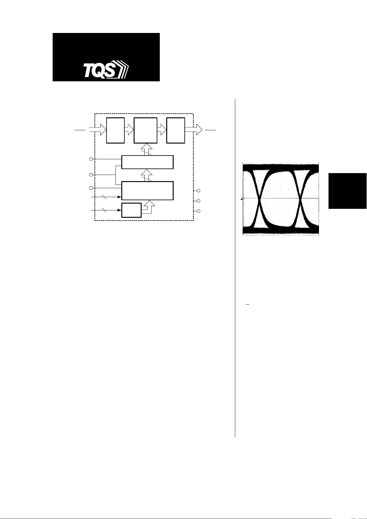
The TQ8016 is a 16 x 16 differential digital crosspoint switch capable of
handling 1.3 Gbit/s data rate. The high data rate and exceptional signal
fidelity is made possible with TriQuint's fully differential Source-Coupled
FET Logic (SCFL) standard cells. The symmetrical switching characteristic
inherent in differential logic results in low signal skew and crosstalk for
maximum signal fidelity.
The user can independently configure any switch output to any input,
including an input chosen by another output. To configure the switch, the
4-bit output address (OA0..3) is decoded to enable the loading of the 4-bit
input selection data (IA0..3) on the rising edge of the LOAD signal. The
process is repeated until all desired connections are programmed. By
bringing the CONFIGURE signal high, the contents of the Output Select
Latches are transferred in parallel to a second row of 4-bit latches (R2),
causing the switch reconfiguration.
This double row architecture minimizes the time to completely reconfigure
the switch since a new set of addresses can be loaded to the Output Select
Latches (R1) while the switch is active (transmitting). At the time of
reconfiguration, no data drop-out occurs for any output whose input
connection does not change.
For applications which do not require synchronous configuration of the
switch, the LOAD and CONFIGURE inputs may be tied together.
Typical output waveform with
all channels driven
Features
• >1.3 Gigabit/sec data rate
• Non-blocking architecture
•
+200 ps delay match (one
input to all outputs)
•
ECL-level data inputs/outputs;
CMOS-level control inputs
• Low crosstalk
• Fully differential data path
• Double row of output select
latches minimizes
reconfiguration time
• Available in 132-pin leaded
chip carrier
Input
Buffers
Output
Buffers
16 x 16
Crosspoint
Switch
Matrix
64
64
(R2)
Sixteen 4-Bit Latches
(R1)
Sixteen 4-Bit Addressable
Output Select Latches
4
4
4:16
Decoder
VCC
VEE
GND
O0..15
O0..15
D0..15
D0..15
CONFIGURE
RESET
LOAD
IA0..3
OA0..3
TQ8016
Page 2
TQ8016
For additional information and latest specifications, see our website: www.triquint.com
3
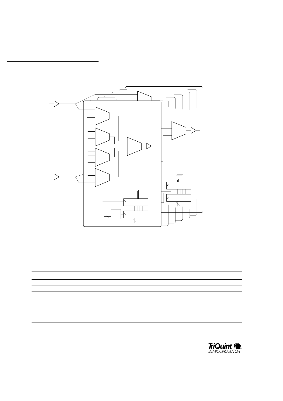
Figure 1. TQ8016 Architecture
Table 1. Pin Descriptions
Pin Name Levels Description
D0–D15 ECL Differential Data Inputs
D0–D15 ECL Differential Data Inputs
D0–D15 ECL Differential Data Inputs
O0–O15 ECL Differential Data Outputs
O0–O15 ECL Differential Data Outputs
IA0–IA3 CMOS Input Address
OA0–OA3 CMOS Output Address
CONFIGURE CMOS Switch Reconfiguration
DATA
OUT 15
(O15)
5
RESET
OUTPUT
SELECT ADDRESS
(OA0:3)
Input
Buffers
DATA
OUT 0
(O0)
Configuration
Register
Program Register
CONFIGURE
LOAD
4
16 X 1-BIT
MULTIPLEXER
16 X 1-BIT
MULTIPLEXER
.
.
.
.
.
.
.
.
.
.
.
.
DATA IN 0
(I0)
DATA IN 15
(I15)
4
INPUT ADDRESS
(IA0:3)
4:16
DECODE
Page 3
TQ8016
SWITCHING
PRODUCTS
3
For additional information and latest specifications, see our website: www.triquint.com
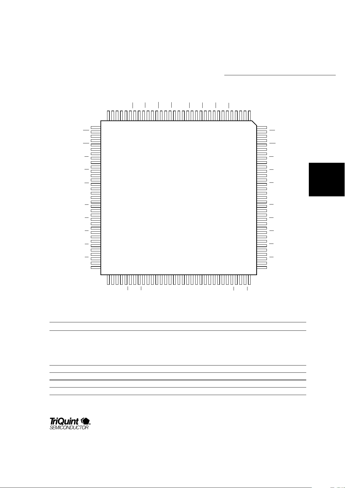
Figure 2. Pinout
VEE
D12
D12
D13
D13
D14
D14
D15
D15
O15
O15
O14
O14
O12
O12
O13
O13
GND
GND
GND
GND
GND
GND
GND
GND
GND
GND
VCC
VCC
O11
O11
O10
O10
O9
O9
O8
O8
O7
O7
GND
GND
GND
GND
O6
O6
O5
O5
O4
O4
O3
O3
O2
O2
GND
GND
VEE
GND
GND
NC
GND
GND
VEE
NCNCGNDO1O1
GNDO0O0
VCC
D1
D1
GND
D0
D0
GND
VCC
D2
D2
GND
D3
D3
GND
D4
D4
GND
D5
D5
GND
D6
D6
GND
NC
GND
D7
D7
GND
D8
D8
GND
D9
D9
GND
D10
D10
GND
D11
D11
VEE
GND
IA3
IA2
GND
IA1
IA0
GNDNCGND
CONFIGURE
LOAD
GND
OA3
OA2
GND
OA1
OA0
NC
NC
NC
NC
RESET
Cavity-Down View
132-Pin Ceramic Chip Carrier
101112131415161718192021222324252627282930313233 123456789
67 68 69 70 71 72 73 74 75 76 77 78 79 80 81 82 83 84 85 86 87 88 89 90 91 92 93 94 95 96 97 98 99
100
101
102
103
104
105
106
107
108
109
110
111
112
113
114
115
116
117
118
119
120
121
122
123
124
125
126
127
128
129
130
131
132
34
35
36
37
38
39
40
41
42
43
44
45
46
47
48
49
50
51
52
53
54
55
56
57
58
59
60
61
62
63
64
65
66
Table 1. Pin Descriptions (continued)
Pin Name Levels Description
RESET CMOS
Configures the switch to
Broadcast
or
Pass-Through
modes, overwriting existing configurations.
Broadcast mode: All output ports are connected to data input port 0.
This mode is selected by applying a RESET “high” pulse with CONFIGURE held “low."
Pass-through mode: I0 is connected to O0, I1 to O1, and so on.
This mode is selected by applying a RESET “high” pulse with CONFIGURE held “high."
LOAD CMOS Loads Input Address
GND 0 V. Ground Reference
VEE –5 V Power Supply
VCC +5 V Power Supply
TQ8016
Page 4

TQ8016
For additional information and latest specifications, see our website: www.triquint.com
3
Symbol Parameter Absolute Max. Rating Notes
T
STOR
Storage Temperature –65° C to +150° C
T
J
Junction Temperature –55° C to +150° C
T
C
Case Temperature Under Bias –55° C to +125° C1
VCCSupply Voltage 0 V to +7 V 2
V
EE
Supply Voltage –7 V to 0 V 2
V
TT
Load Termination Supply Voltage VEE to 0 V 3
V
IN
Voltage Applied to Any ECL Input; Continuous VEE –0.5 V to +0.5 V
I
IN
Current Into Any ECL Input; Continuous –1.0 mA to +1.0 mA
V
IN
Voltage Applied to Any TTL/CMOS Input; Continuous –0.5 V to VCC +0.5 V
I
IN
Current Into Any TTL/CMOS Input; Continuous –1.0 mA to +1.0 mA
V
OUT
Voltage Applied to Any ECL Output VEE –0.5 V to +0.5 V 3
I
OUT
Current From Any ECL Output; Continuous –40 mA
P
D
Power Dissipation per Output P
OUT
= (GND – V
OUT
) x I
OUT
50 mW
Table 2. Absolute Maximum Ratings
4
Notes: 1. TC is measured at case top.
2. All voltages specified with respect to GND, defined as 0V.
3. Subject to I
OUT
and power dissipation limitations.
4. Absolute maximum ratings, as detailed in this table, are the ratings beyond which the device's performance may be
impaired and/or permanent damage to the device may occur. Functionality and/or adherence to electrical
specifications is not implied when the device is subjected to conditions that exceed, singularly or in combination, the
operating range specified in the Recommended Operating Conditions table, below.
.
Table 3. Recommended Operating Conditions
3
Notes: 1. TC measured at case top. Use of adequate heatsink is required.
2. The V
TT
and R
LOAD
combination is subject to maximum output current and power restrictions.
3. Functionality and/or adherence to electrical specifications is not implied whenthe device is subjected
to conditions that exceed, singularly or in combination, the operating ranges specified.
Symbol Parameter Min. Typ. Max. Units Notes
T
C
Case Operating Temperature 0 25 85 °C1
GND Ground Reference Voltage 0 V
V
CC
Supply Voltage 4.5 5.5 V
V
EE
Supply Voltage –5.5 –4.5 V
V
TT
Load Termination Supply Voltage –2.0 V 2
R
LOAD
Output Termination Load Resistance 50 Ω 2
Page 5

TQ8016
SWITCHING
PRODUCTS
5
For additional information and latest specifications, see our website: www.triquint.com
Symbol Parameter Min Typ Max Units Test Cond. Notes
V
IH
ECL Input Voltage High –1100 –500 mV
V
IL
ECL Input Voltage Low V
TT
–1500 mV
I
IH
ECL Input Current High +30 uA VIH = 0.7 V
I
IL
ECL Input Current Low –30 uA VIL = –2.0 V
V
ICM
ECL Input Common Mode Voltage –1500 –1100 mV
V
IDIF
ECL Input Differential Voltage (P–P) 400 1200 mV
V
IH
CMOS Input Voltage High 3.5 V
CC
V
V
IL
CMOS Input Voltage Low 0 1.5 V
I
IH
CMOS Input Current High +100 uA VIH = V
CC
I
IL
CMOS Input Current Low –100 uA VIL = 0 V
V
OCM
ECL Output Common Mode –1500 –1100 mV
V
ODIF
ECL Output Differential Voltage 600 mV
V
OH
ECL Output Voltage High –1000 –600 mV
V
OL
ECL Output Voltage Low V
TT
–1600 mV
I
OH
ECL Output Current High 20 23 27 mA
I
OL
ECL Output Current Low 0 5 8 mA
I
CC
Power Supply Current 15 20 mA 2
I
EE
Power Supply Current 730 950 mA 2
Table 4. DC Characteristics
1
TC = 0 °C to 85 °C, VCC = 4.5 V to 5.5 V, VEE = –5.5 V to –4.5 V, GND = 0 V, unless otherwise indicated.
Notes: 1. Test conditions unless otherwise indicated: VTT = –2.0 V, R
LOAD
= 50 Ω to V
TT.
2. Positive current is defined as flowing into the device and negative current as flowing out of the device.
I
CC
typically flows into the device and IEE flows out of the device.
Notes: 1. Test conditions: V
TT
= –2.0 V, R
LOAD
= 50 Ω to VTT; ECL inputs: VIH = –1.1 V; VIL = –1.5 V; CMOS inputs: VIH = 3.5 V, VIL = 1.5 V;
ECL outputs: V
OH
> –1.0 V, VOL < –1.6 V; ECL inputs rise and fall times < 1 ns; CMOS inputs rise and fall times < 20 ns. A bit error
rate of 1E – 13 BER or better for 2
23
– 1 PRBS pattern, jitter and rise/fall times are guaranteed through characterization.
2. 1.2 Gb/s Non-Return-Zero (NRZ) data equivalent to 600 MHz clock signal.
3. Rise and fall times are measured at the 20% and 80% points of the transition from V
OL
max to VOL min.
Symbol Parameter Min Typ Max Units Notes
Maximum Data Rate/Port 1.3 Gb/s 1,2
Jitter 150 ps pk–pk 1
T
1
Channel Propagation Delay 1200 2000 ps
T
2
Ch-to-Ch Propagation Delay Skew 400 500 ps
T
3
CONFIG to Data Out (Oi) Delay 5 ns
T
4
LOAD Pulse Width 7 ns
T
5
CONFIG Pulse Width 7 ns
T
6
IAi to LOAD High Setup Time 0 ns
T
7
LOAD to IAi Low Hold Time 3 ns
T
8
OAi to LOAD High Setup Time 0 ns
T
9
LOAD to OAi Low Hold Time 3 ns
T
10
Load ↑ to CONFIG ↑ 0ns
T
11
RESET Pulse Width 10 ns
T
R,F
Output Rise or Fall Time 250 400 ps 3
Table 5. AC Characteristics1 – Within recommended operating conditions, unless otherwise indicated.
Page 6

TQ8016
For additional information and latest specifications, see our website: www.triquint.com
3
Figure 3. Timing Diagram — Switch Configuration
Figure 4. Timing Diagram — Reset
Notes: 1. LOAD input must remain LOW to insure correct programming of the switch
2. "Broadcast" is defined as data input 0 to all data outputs (0..15).
3. "Pass-through" is defined as data input 0 to data output 0, data input 1 to data output 1, etc.
Output
Address
Input
Address
LOAD
CONFIGURE
A
D
B
D
C
D
D
D
E
D
F
D
G
D
A
O
B
O
C
O
D
O
E
O
F
O
G
O
T8 T7
T5
T6
T1
T9
T3
Invalid
Data Out
T10
T4
Data
In
Data
Out
Output
Data
RESET
CONFIGURE
T11
Broadcast Pass-through
Page 7

TQ8016
SWITCHING
PRODUCTS
7
For additional information and latest specifications, see our website: www.triquint.com
Figure 5. AC Performance Measurements
Typical Error-Free Area
The graph in Figure 5 shows the typical error-free area
of a 2
23
– 1 Pseudo-Random Bit Stream (PRBS) "eye"
pattern. Data is provided for both time and voltage
domains of the differential DIN0 to DOUT0 data path for
various data rates. An interference pattern was applied
to all other inputs in parallel to induce worst-case cross
talk.
For the time domain, Peak-to-Peak Jitter was measured
at the eye crossing.
(Percent Recoverable "Eye" vs. Frequency 16 x 16)
100
90
80
70
60
50
40
30
20
10
0
200
300
400
500
600
700
800
900
1000
1100
1200
1300
1400
1500
1600
1700
1800
1900
2000
2100
2200
Time Domain
Voltage (Inner Eye)
Frequency (Mb/s)
Percent (%)
An error-free percentage value was computed using the
following formula:
(Data_Period - PPJitter) x 100 / Data_Period
Voltage values are referenced to an initial inner eye
measurement at 400 MBs. Subsequent percentage
values were computed using the following formula:
V
INNER
x 100 / V
INNER
@ 400 MBs
Page 8
TQ8016
For additional information and latest specifications, see our website: www.triquint.com
3
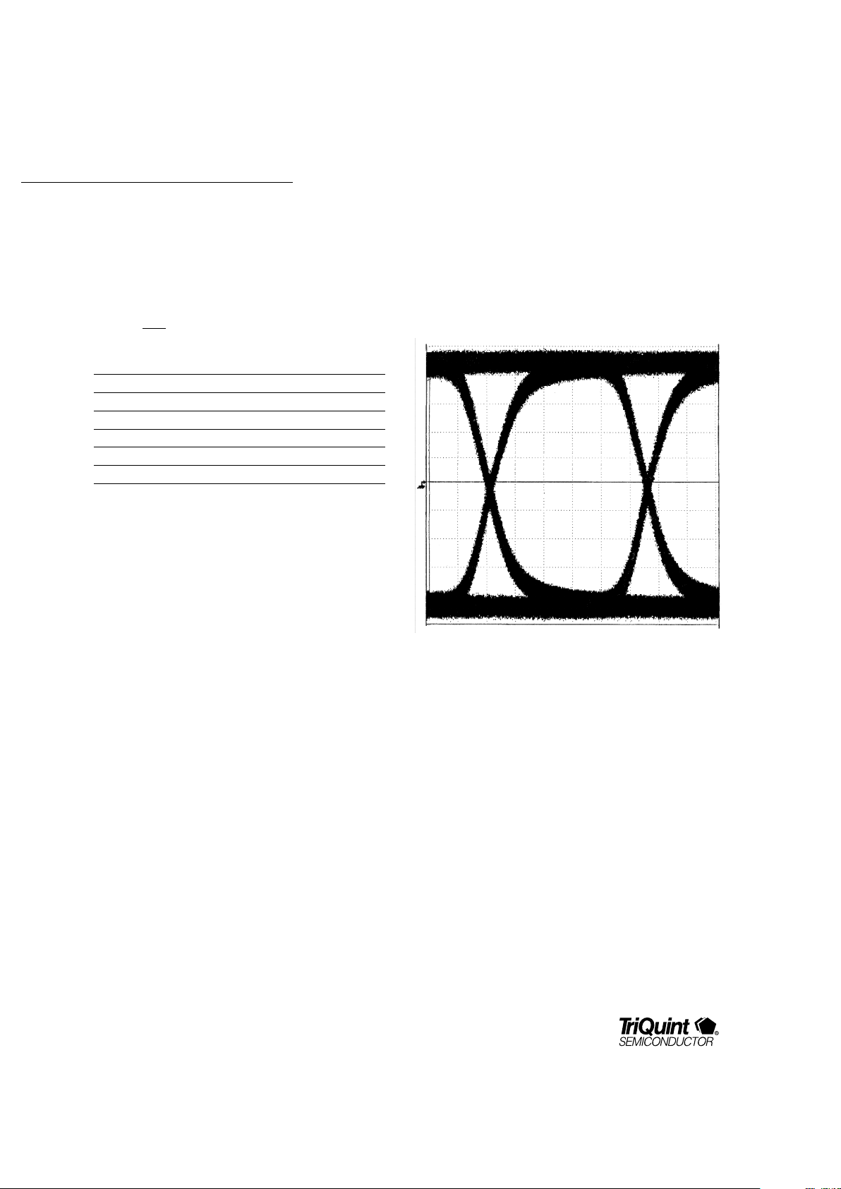
Figure 5. 1200 Mb/s Data "Eye" PatternTable 6. Typical Differential Waveform Characteristics
(OUT – OUT)
Time/Div: 150 ps
Frequency 1200 Mb/s
Fall Time (20% – 80%) 195 ps
Rise Time (20% – 80%) 1200 Mb/s
Jitter (peak-to-peak) 40 ps
Time/division 125 ps
Volts/division 250 mV
Page 9
TQ8016
SWITCHING
PRODUCTS
9
For additional information and latest specifications, see our website: www.triquint.com
Ordering Information
TQ8016-M
1.3 Gb/s 16x16 ECL Crosspoint Switch
Additional Information
For latest specifications, additional product information,
worldwide sales and distribution locations, and information about TriQuint:
Web: www.triquint.com Tel: (503) 615-9000
Email: sales@tqs.com Fax: (503) 615-8900
For technical questions and additional information on specific applications:
Email: applications@tqs.com
The information provided herein is believed to be reliable; TriQuint assumes no liability for inaccuracies or
omissions. TriQuint assumes no responsibility for the use of this information, and all such information
shall be entirely at the user's own risk. Prices and specifications are subject to change without notice.
No patent rights or licenses to any of the circuits described herein are implied or granted to any third party.
TriQuint does not authorize or warrant any TriQuint product for use in life-support devices and/or systems.
Copyright © 1997 TriQuint Semiconductor, Inc. All rights reserved.
Revision 1.1.A November 1997
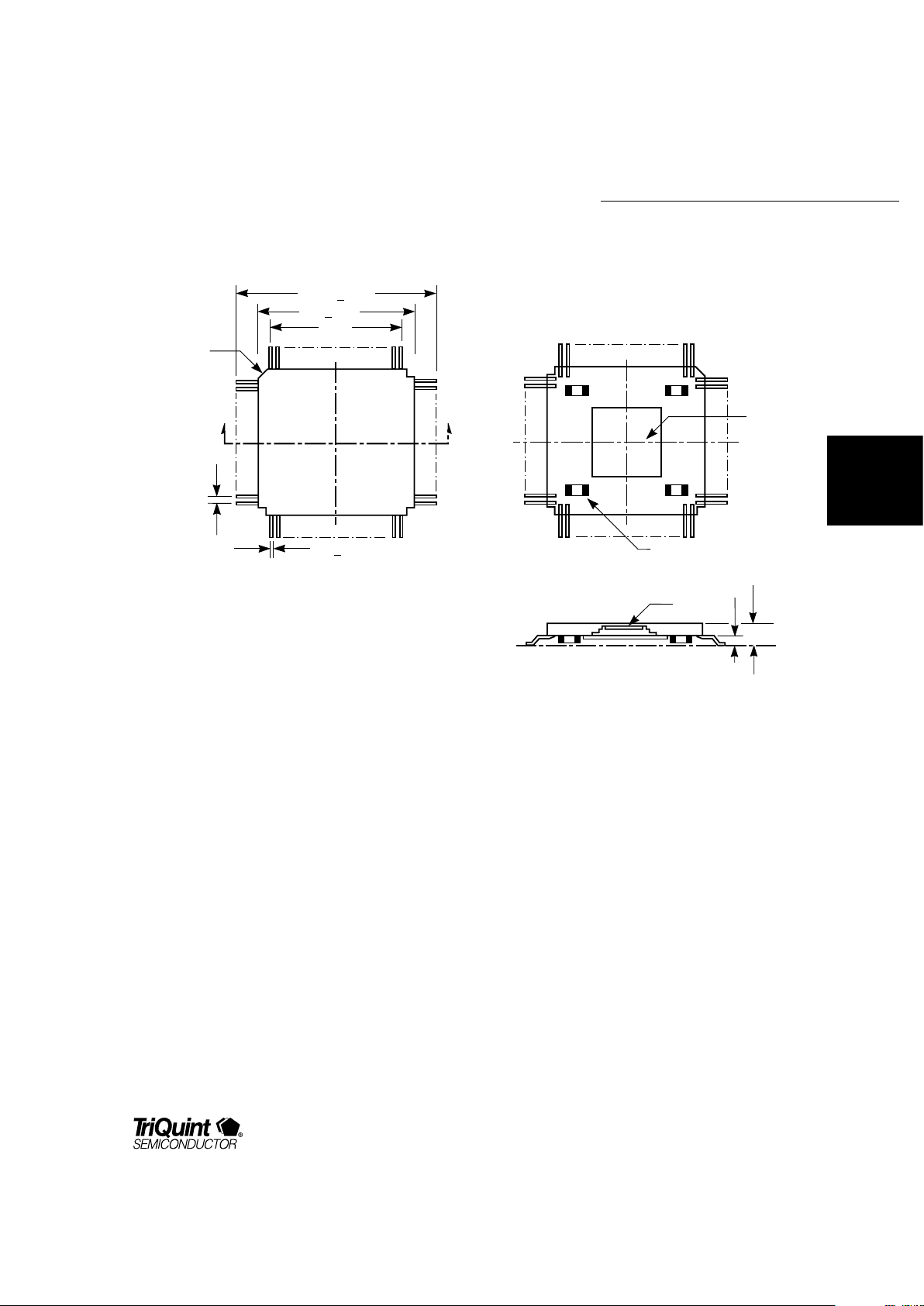
Top View Bottom View
Section A-A
.010 +.0015
BSC
1.170 +.006
PIN 1
INDEX
.950 +.006
.800
132
1
A
A
.025
DEVICE
.125
SEATING PLANE
.064
CERAMIC OR
METAL LID
CHIP CAPACITOR, 4 PLACES
Figure 6. Mechanical Dimensions
 Loading...