

Page 1
T R I Q U I N T S E M I C O N D U C T O R , I N C .
1
For additional information and latest specifications, see our website: www.triquint.com
MIXED SIGNAL
PRODUCTS
TQ6124
1 Gigasample/sec,
14-bit
Digital-to-Analog
Convertor
The TQ6124 is a 14-bit monolithic digital-to-analog converter. The TQ6124
achieves conversion accuracy by using a segmented architecture, precision
current sources, and on-chip nichrome resistors. The only external
components required are an external reference and loop control amplifier.
The TQ6124 is ideally suited for applications in direct digital synthesis,
pixel generation for high-resolution monitors, broadband video generation,
and high-speed arbitrary waveform generators.
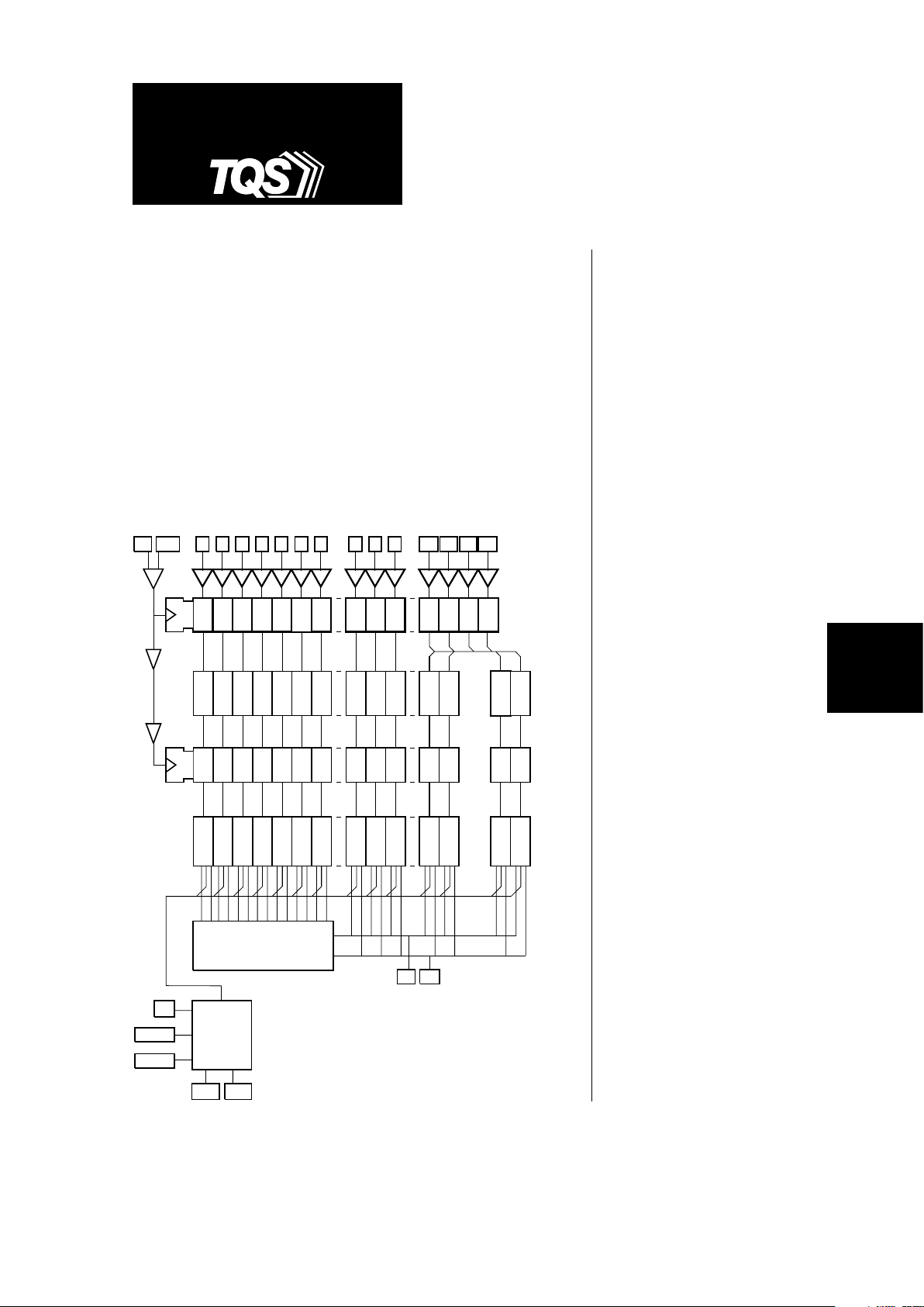
Figure 1. TQ6124 Block Diagram
Features
• 1Gs/s aggregate bandwidth
• 14-bit resolution
• RF front end
• ECL-compatible inputs
• 0.026% DC differential
non-linearity
• 0.035% DC integral non-linearity
• SFDR: 52 dBc @ F
OUT
= 75 MHz
48 dBc @ F
OUT
= 148 MHz
45 dBc @ F
OUT
= 199 MHz
• 1.4 W power dissipation
• 44-pin ceramic QFP package
or die only
Applications
• Direct Digital Synthesis
• Pixel generation for workstations
and high-end monitors
• Direct-generation of broadband
video for cable TV
• High-speed arbitrary waveform
generators
Master
Latch
Segment
Encoders
Delay
Stages
D4 D5 D6 D7 D8 D9 D10 D11 D12 D13
CLK
NCLK
LSBs Intermediate Bits
MSBs
D0 D1 D2 D3
S1 S2
S14 S15
Slave
Latch
...
Current
Switches
Current
Source
Array
V
O
NV
O
V
REF
V
SENSE
50 ohm R-2R Ladder Network
V
AA
MID_trim
LSB_trim
...
...
Page 2
TQ6124
2
For additional information and latest specifications, see our website: www.triquint.com
Functional Description
The TQ6124 registers incoming bits in a master latch
array. The value of the four most-significant bits is
encoded into an n-of-15 thermometer code while the ten
low-order bits pass though an equalizing delay stage. All
25 bits are re-registered in a 25-wide slave latch array
which drives a set of 25 differential pair switches. These
switches steer the corresponding segment and bit
currents into the true (V
O
) and complementary (NVO)
outputs. This architecture minimizes glitch impulses by
eliminating large mid-scale current transitions.
The most-significant bits generate the segment
currents, which are of equal weight at
1
/16 of the full-
scale output (I
FS
). The ten lower-order bits are divided
into two subgroups. The three intermediate bits steer
binary-weighted currents of magnitude I
FS
/32, IFS/64
and I
FS
/128 to the outputs. The seven least-significant
bits steer identical I
FS
/128 currents into a differential
R-2R ladder to generate effective bit currents of I
FS
/256
to I
FS
/16384. The DAC output is the sum of the
outputs of the segments and the low-order bits.
Clock and data inputs are ECL-compatible. The outputs
are designed to operate into a 50Ω load, with internal
reverse termination to ground being provided by the
R-2R network.
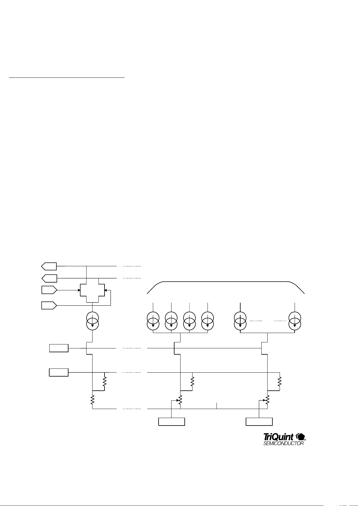
External compensation is utilized to minimize the effects
of device mismatch. An external op amp senses the sum
of the segment, the intermediate bit, and the LSB currents.
Figure 2. TQ6124 Currents
Q
V
O
NQ
NV
O
Segments 1 thru 15
2.5mA
R
SENSE
5.8KΩ
R
SOURCE
1.2KΩ
R
SENSE
5.8KΩ
R
SOURCE
1.2KΩ
1.25mA
.625mA
.3125mA
.3125mA
I
D9
dummy
I
D7
I
D8
R
SENSE
5.8KΩ
R
SOURCE
1.2KΩ
.3125mA
.3125mA
I
D6
dummy
(x8)
To switches for D0 thru D9
MID_trim
LSB_trim
V
AA
V
SENSE
V
REF
Page 3
TQ6124
3
For additional information and latest specifications, see our website: www.triquint.com
MIXED SIGNAL
PRODUCTS
Electrical Specifications
Table 1. Recommended Operating Conditions
Symbol Parameter Min. Nom. Max. Unit
V
SS
Negative Power Supply –5.25 –5.0 –4.75 V
V
AA
Analog Power Supply –15.5 –12 –11.5 V
T
C
Case Temperature –20 85 °C
Table 2. DC Operating Characteristics
Unless otherwise specified, measured over Recommended Operating Conditions with balanced 50Ω loads, V
FS
= 1.0 V.
Symbol Parameter Condition Min. Nom. Max. Unit
I
AA
VAA Supply Current –75 –90 mA
I
SS
VSS Supply Current –285 –450 mA
V
REF
Reference Voltage V
AA
+ 2.5 VAA + 3.0 V
AA
+ 3.75 V
I
REF
Reference input current –25 25 mA
V
IH
ECL Input High Voltage V
EREF
= –1.3 V –1.1 –0.6 V
V
IL
ECL Input Low Voltage V
EREF
= –1.3 V –2.5 –1.5 V
I
I
ECL Input Current –25 25 mA
V
EREF
ECL Reference Voltage V
SS
= –5.0 V –1.34 V
R
EREF
ECL Reference Resistance 400 ohms
DNL Differential non-linearity (Note 2) –0.05 0.026 0.05 %F.S.
INL Integral non-linearity (Note 2) –0.05 0.035 0.05 %F.S.
Full-scale symmetry (Note 1) –8 2 8 mV
V
FS
Full-scale output voltage RL = 50 ohms –1.0 –1.125 V
R
OUT
VO, NVO, output resistance 44 50.9 57 ohms
R
OUT
Matching –2.5 0.15 2.5 %
VO, NV
O
Output Voltage –1.125 0 V
V
ZS
Zero Scale Voltage –50 –40 0 mV
V
SENSE
Sense output voltage V
AA
+ 2.5 V
AA
+ 3.75 V
θ
JC
Thermal Impedance 15 °C/W
Notes: 1. Full-scale symmetry is a measure of the balance between VO and NVO. For a full-scale output transition,
the change in V
O
will match the change in NVO to within the specified amount. Any imbalance in the
output loads will affect symmetry.
2. Linearity can interpreted as 10 bits at
1
/2 LSB or as 11 bits at 1 LSB. The device is monotonic to 10 bits.
Linearity is tested with the Mid_trim set for optimal DNL, with the LSB_trim pin open.
Page 4

TQ6124
4
For additional information and latest specifications, see our website: www.triquint.com
Table 3. AC Operating Characteristics
Unless otherwise noted, measured over DC operating characteristics with balanced 50Ω loads,
V
FS
= 0.8V, V
IN
= 0.8V
P-P
, input rise and fall times ≤ 300 ps.
Symbol Parameter Condition Min. Typ. Max. Unit
F
CLK
Clock Frequency 50 1000 MHz
tR, t
F
At full scale 10% to 90% 350 ps
t
DS
Data Setup Time 200 ps
t
DH
Data Hold Time 300 ps
t
CLKHI
Clock High Time 400 ps
t
CLKLO
Clock Low Time 400 ps
SFDR* Spurious free dynamic range F
OUT
= 75 MHz 45 52 dBc
F
OUT
= 148 MHz 45 52 dBc
F
OUT
= 199 MHz 45 49 dBc
*Note: SFDR testing performed at F
CLK
= 600 MHz only.
Table 4. Absolute Maximum Ratings
Symbol Parameter Min. Max. Unit
V
SS
Digital Supply –7.0 V
V
AA
Analog Supply –16.0 V
VO, NV
O
Analog Output Voltage –2.0 2.0 V
VI Digital Input Voltage VSS – 0.5 +0.5 V
II Digital Input Current –1.0 +1.0 mA
V
REF
Reference Voltage VAA-2 0 V
I
REF
Reference Current –1 1 mA
Power Dissipation 5 W
T
STG
Storage Temperature –65 150 °C
T
J
Operating Junction Temperature 150 °C
Note: Absolute Maximum Ratings are those beyond which the integrity of the device cannot be guaranteed.
If the device is subjected to the limits in the absolute maximum ratings, its reliability may be impaired.
The Electrical Specifications tables provide conditions for actual device operation.
Page 5

TQ6124
5
For additional information and latest specifications, see our website: www.triquint.com
MIXED SIGNAL
PRODUCTS
Operating Notes
Current Source Control Loop
The full scale output voltage is set through the use of
an external op amp, as shown in Figure 4. Nominal full
scale output voltage can be achieved by using a voltage
source. With this, control voltages on the op amp of
around V
AA
+3V can be set. Adjusting the full scale
output voltage can be achieved by toggling the inputs
over full scale while adjusting the control voltage to
achieve the desired level.
AC Timing
The low-going transition of CLK latches the data.
Production SFDR testing is performed with the clock
transitioning in the center of the data eye. The timing of
the clock transition with respect to the data can
improve SFDR performance.
Systems working to
optimize SFDR can 'tune' this phase relationship to
optimize the desired characteristic.
V
REF
Adjustment Range
The output full scale voltage range can be set through
the V
REF
input. Figure 5 shows the approximate
relationship between V
REF
and VFS.
Figure 4. Adjusting the Full-Scale Output Voltage
Figure 5. Full-Scale Output Voltage vs. V
REF
0.2
0.4
0.6
0.8
1.0
1.2
–1
01234
Reference Voltage (vs VAA)
Full-Scale Output Voltage
Figure 3. AC Timing Relationships
DS
t
DH
t
Data
Clock
–
+
V
AA
V
SENSE
V
REF
1KΩ
20 KΩ
1 KΩ
MC34071
620 Ω
AD586
LSB_TRIM
MID_TRIM
1 KΩ
1 KΩ
V
AA
20 KΩ
+V
IN
V
OUT
V
AA
20 KΩ
V
AA
Page 6

TQ6124
6
For additional information and latest specifications, see our website: www.triquint.com
Operating Notes (continued)
Power Supplies
Optimized performance depends on clean supplies.
Utilize very low impedance negative supplies that are
decoupled over a wide frequency range. The analog and
digital grounds should be isolated at the chip, connecting
to a single point ground on the circuit board.
ECL Reference
The single-ended data inputs switch against an internal
reference of -1.3V (nominal). Variations among input
buffers, or in V
TT
, may benefit from adjustments in the
reference. The ECL reference pin may be driven externally.
Its equivalent load is 400 ohms to –1.3V (nominal).
Trim Adjustments
The external trim adjustments for the midrange bits
and the LSBs is optional. Trimming is performed by
monitoring the attribute of greatest concern (INL, DNL,
Spurious levels) while minimizing the unwanted effects.
Trim inputs should be left open if not used.
Signals
Figure 6. TQ6124 Pinout
33
V
SS
32
D
2
31
D
1
30
D (LSB)
0
29
DGND
28
DGND
27
ECLref
26
LSBtrim
24
V
AA
25
Midtrim
23
V
AA
44
V
SS
43
D
9
42
D
8
41
D
7
40
DGND 39D
6
38
D
5
37
DGND35D
3
36
D
4
34
V
SS
V
SS
12
AGND
13
I
REF
14
AGND
15
NV
O
16
V
O
17
AGND18AGND19V
REF
21
V
SNS
20
V
AA
22
V
SS
1
D
10
2
D
11
3
D
12
4
D13(MSB) 5
DGND 6
DGND 7
DGND 8
NCLK
10
CLK 9
V
SS
11
TQ6124
Top View
Page 7

TQ6124
7
For additional information and latest specifications, see our website: www.triquint.com
MIXED SIGNAL
PRODUCTS
Table 5. Signal-Pin Descriptions
Signal Pin(s) Description
DGND 6, 7, 8, 28, 29, 37, 40 Ground connection for digital circuitry.
AGND 13, 15, 18, 19 Ground connection for analog circuitry.
D0 thru D
13
30, 31, 32, 35, 36, 38, 39, Data inputs. D0 is the least significant bit. ECL levels.
41, 42, 43, 2, 3, 4, 5
VO, NV
O
17, 16 True and complementary analog outputs.
CLK, NCLK 9, 10 True and complementary clock inputs. ECL levels.
I
REF
14 Connect to AGND. Source of dummy currents in the switch array.
V
SENSE
20 Sense Output.
V
REF
21 Reference Input.
V
SS
1, 11, 12, 33, 34, 44 Digital negative power supply.
V
AA
22, 23, 24 Analog negative power supply.
Mid_trim 25 Trim terminal for mid range bits.
LSB_trim 26 Trim terminal for LSB range bits.
ECLref 27 Optional ECL reference level adjustment. Thevinin equivalent is 1.3V
nominally into 400 ohms. Equivalent voltage tracks with digital supply.
Typical Performance Data
The graph in Figure 7 shows representative
performance data of spurious free dynamic range
(SFDR) vs. output frequency performance measured
from TQ6124 devices.
Data was collected at room temperature; note,
however, that SFDR is not strongly dependendent on
temperature. Optimum performance is obtained by
utilizing as high a clock rate as practical.
Figure 7. SFDR vs. Output Frequency
–30
–35
–40
–45
–50
–55
–60
–65
50 100 150 200 250 300 350 400 450 500
0
F
OUT
SFDR
Page 8

TQ6124
8
For additional information and latest specifications, see our website: www.triquint.com
Packaging
Figure 8. 44-pin QFP Package Dimensions
Section A-A
Top View
BottomView
.015
BSC
0.805
Pin 1
Index
.650
44
1
A
A
.050
All dimensions in inches
Ceramic or
metal lid
Device
.125
Seating plane
.065
.035 typ.
Page 9

TQ6124
9
For additional information and latest specifications, see our website: www.triquint.com
MIXED SIGNAL
PRODUCTS
Ordering Information
TQ6124-CM
1 GS/s 14-bit DAC in 44-pin ceramic QFP
TQ6124-CD
1 GS/s 14-bit DAC — die only
ETF6124
Engineering Test Fixture with TQ6124 device
Additional Information
For latest specifications, additional product information,
worldwide sales and distribution locations, and information about TriQuint:
Web: www.triquint.com Tel: (503) 615-9000
Email: sales@tqs.com Fax: (503) 615-8900
For technical questions and additional information on specific applications:
Email: applications@tqs.com
The information provided herein is believed to be reliable; TriQuint assumes no liability for inaccuracies or
omissions. TriQuint assumes no responsibility for the use of this information, and all such information
shall be entirely at the user's own risk. Prices and specifications are subject to change without notice.
No patent rights or licenses to any of the circuits described herein are implied or granted to any third party.
TriQuint does not authorize or warrant any TriQuint product for use in life-support devices and/or systems.
Copyright © 1997 TriQuint Semiconductor, Inc. All rights reserved.
Revision 1.1.A November 1997
 Loading...