

Page 1
T R I Q U I N T S E M I C O N D U C T O R , I N C .
1
For additional information and latest specifications, see our website: www.triquint.com
MIXED SIGNAL
PRODUCTS
Features
• 1 Gs/s conversion rate
• 8-bit resolution
• DC differential non-linearity
1
/2 LSB (0.2%)
• DC integral non-linearity
1 LSB (0.4%)
• Settling time 2 ns to 0.4% (est.)
• Spurious-free dynamic range
(SFDR) 45 dBc typical
• ECL-compatible inputs
• Synchronous blanking input
• 1.3 W power dissipation
• 44-pin multilayer ceramic
package or unpackaged die
Applications
• Display generation
• Waveform and signal synthesis
• Video signal reconstruction
BLANK
A5 A6
B6
A7 (MSB)
B7
MULTIPLEXER
ECL INPUT
BUFFERS
BLANKING
LOGIC
MASTER
LATCH
SLAVE
LATCH
V
(-5 V)
A
BLANK DISABLE
V
V
I
V
BANDGAP
REFERENCE
FULL-SCALE ADJUST
V
CLK
CLK
SELA
BLANK D0 D4
QBLANK Q0 Q4
D5 D6 D7
Q5 Q6 Q7
BINARY-TO-N-OF-7
SEGMENT ENCODER
S1 S2 S3 S4 S5 S6 S7
QS1
QS7
+
–
I
I4
IS1
IS7
+
–
CURRENT-SOURCE ARRAY
50
50
OUT
V
OUT
V
B5B4
BLANK
I0
SENSE
REF
B0
A0
A4
GND
GND
SS
AA
AA
REF
D Q
(-5V)
(EXT. CONTROL LOOP)
D
BLANK D0 D4
QBLANK Q0 Q4
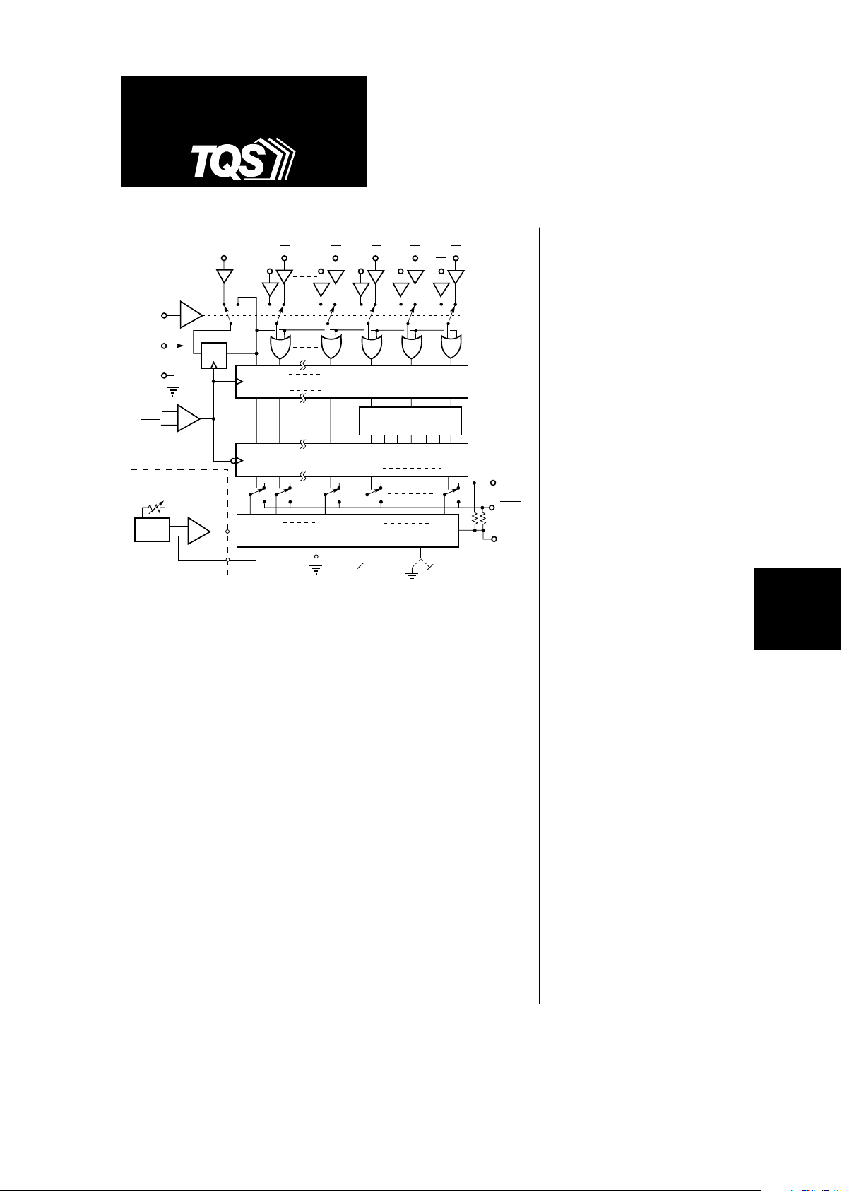
TriQuint's TQ6122 GIGADAC™ is a monolithic, 8-bit digital-to-analog
converter capable of conversion rates to at least 1000 Megasamples/
second. The TQ6122 DAC may be used for display generation, waveform
and signal synthesis, and video signal reconstruction. The TQ6122 features
a 2:1 data MUX at the input for ease of interface and offers synchronous
blanking capability for maximum ease of use in video applications. It drives
complementary 1 V peak-to-peak swings into 50-ohm loads; on-chip 50ohm reverse terminations provide extremely fast settling time.
Due to the inherently high speed of TriQuint's one-micron gate
Enhancement / Depletion-mode gallium arsenide process, the TQ6122
offers guaranteed operation at clock rates of 1000 MHz, with typical room
temperature conversion rates of 1.5 Gs/s without multiplexing and 1.3 Gs/s
when using multiplexed inputs. The TQ6122 features output rise and fall
times of 500 ps (10% – 90%), symmetric complementary output transitions,
and glitch impulse values less than 10 pV/sec. When used for sine wave
synthesis, typical spurious and harmonic free dynamic range is ≥45 dBc.
The TQ6122 may be retrofitted into designs which currently use TriQuint's
TQ6111, 2, 3, 4M DACs with minimal changes to power supply levels and
input and output connections. The part is available in a 44-pin ceramic
package or as unpackaged die.
TQ6122
1 Gigasample/sec,
8-bit Digital-to-Analog
Converter
Page 2
TQ6122
2
For additional information and latest specifications, see our website: www.triquint.com
Specifications
Table 1. Absolute Maximum Ratings
(1,2)
Symbol Description Min Typ Max Units
A
GND
, D
GND
Analog and digital ground –2 +2 V
V
SS
Digital power –7 V
V
AA
Analog power –10 V
VO, VO (MAX) Analog output (1 V F.S.) –2.5 +2.5 V
VI (MAX) Digital input levels VSS –0.5 +0.5 V
II (MAX) Digital input currents –1 +1 mA
P
D
Power dissipation 3.0 W
T
C
Case backside temperature –65 +135 °C
T
S
Storage temperature –65 +150 °C
Notes: 1. Unless otherwise specified: A
GND
= D
GND
= 0 V, VSS = VAA = –5 V, VFS = 1 V pk–pk, case temperature = 27 °C.
2. Exceeding the absolute maximum ratings may damage the device. The value shown for a particular
parameter is determined with all other parameters at their nominal values.
Table 2. DC Characteristics
(1)
Symbol Description Test Conditions Min. Typ. Max. Unit
V
AA
Analog supply Note 2 –5.25 –4.75 V
I
AA
VAA current VFS = 1 V pk–pk 50 62 80 mA
V
SS
Digital supply Note 2 –5.5 –4.5 V
I
SS
VSS current 145 200 265 mA
P
D
Power dissipation 0.9 1.3 1.85 W
V
ECLREF
ECL reference level Note 3, Figure 1 –1.5 –1.3 –1.1 V
I
ECLREF
ECL ref. input bias current Note 3, Figure 1 ∆V
ECLREF
= ±0.2 V –5 0 +5 mA
R
ECLREF
ECL ref. input resistance Figure 1 50 Ω
C
ECLREF
ECL ref. input capacitance 2 pF
VIH(DC) Data input HIGH (ECL) DC value (V
ECLREF
= –1.3 V) –1100 –500 mV
VIL(DC) Data input LOW (ECL) DC value (V
ECLREF
= –1.3 V) V
TT
–1500 mV
V
CLKH
(DC), Clock HIGH input Differential clock, Note 4 V
ECLREF
+0.3 –0.7 V
V
CLKH
(DC)
V
CLKL
(DC), Clock LOW input Differential clock, Note 4 V
TT
V
ECLREF
–0.3 V
V
CLKL
(DC)
I
IN
Data, clock input bias current VIH = –800 mV, VIL = –1800 mV –25 +25 uA
C
IN
Data, clock input capacitance In multilayer ceramic package 0.5 pF
V
OUT
(MAX), Maximum absolute output level Note 5 +1 V
V
OUT
(MAX)
V
OUT
(MIN), Minimum absolute output level Note 5 –1.5 V
V
OUT
(MIN)
(Continued on next page)
Page 3
TQ6122
3
For additional information and latest specifications, see our website: www.triquint.com
MIXED SIGNAL
PRODUCTS
V
FS
Full-scale output swing Data bits only, 0–0/1–1 input step 0 1 1.125 V pk–pk
RL = 50 Ω load
V
ZS
Zero-scale offset VFS = 1 V, no external offset, –35 mV
V
BLANK_DISABLE
= 0 V
∆DV
BLANK
Blanking interval Blank input = 1, Notes 6, 7 9 10.4 12 %V
FS
V
BLANK_DISABLE
Blank current disable control Blank current ON –5 (VAA)V
Blank current OFF 0 (A
GND
)V
V
REF
V
REF
input voltage VFS = 1 V peak-to-peak V
AA
+0.7 V
AA
+1.0 V
AA
+1.4 V
VFS = 0 V peak-to-peak V
AA
–1 V
V
SENSE
V
SENSE
output VFS = 1 V peak-to-peak V
AA
+0.8 V
AA
+1.1 V
I
VREF
V
REF
input current V
REF
= V
AA
+0.65 10 uA
V
REF
= V
AA
+1.1 1 mA
I
REF
Ext. reference current output VFS = 1 V peak-to-peak 2 2.5 5 mA
V
IREF
I
REF
terminal voltage –1.5 +1 V
R
OUT, ROUT
V
OUT, VOUT
output resistance 44 50 57 Ω
Matching of R
OUT, ROUT
0.2 2.5 %
C
OUT
V
OUT, VOUT
output capacitance 0.3 pF
Resolution 8 Bits
Monotonicity 8 Bits
DNL Differential non-linearity (± 1/2 LSB) 0.2 % F.S.
INL Integral non-linearity (± 1 LSB) 0.4 % F.S.
Full-scale symmetry VFS = 1 V peak-to-peak, Note 8 –4 +4 mV
VFS temperature coefficient Note 9
Notes: 1. Unless otherwise specified: VAA = –5V ± 5%, VSS = –5 V ±10%, VTT = –2V ± 5%, VFS = 1 V pk–pk, T
CASE
= 0 to +85 °C
2. See the "Power Supplies, Ground and Bypassing" section later in this datasheet for discussion of power supplies.
3. The ECL reference input establishes the switching point for the ECL line receivers used at the DATA, BLANK, and
SELECT inputs. (See Figure 1.) I
ECLREF
is the current required to change the internal ECLREF value by about ±200 mV.
4. Values shown are for differential clock drive, and apply to both CLOCK and CLOCK inputs. For single-ended drive,
the HIGH level should be at least (V
ECLREF
+0.5) volts, but must not exceed –700 mV. The LOW level should be
(V
ECLREF
–0.5) volts, but must not go below VTT, where VTT is the ECL termination voltage (nominal VTT = –2 V).
5. V
OUT
(
MAX
), V
OUT
(
MAX
), V
OUT
(
MIN
), V
OUT
(
MIN
) represent the limits on the absolute output levels, including offset.
6. Blanking interval is the voltage change (as a percentage of the full-scale output swing) added to V
FS
when BLANK is asserted.
7. The BLANK DISABLE input turns OFF the blank current (DV
BLANK
= 0) when held at A
GND
, and turns it ON when pulled to VAA.
8. Full-scale symmetry is a measure of the balance between V
OUT
and V
OUT
. For a full-scale input change (00000000 –> 1111111),
␣␣␣␣the change in V
OUT
will match the change in V
OUT
to within ± 4 mV (1 LSB @ 1 V peak-to-peak).
9. The VFS temperature coefficient is determined primarily by the external reference and loop control op amp.
Table 2. DC Characteristics
(1)
(continued)
Symbol Description Test Conditions Min Typ Max Unit
Page 4

TQ6122
4
For additional information and latest specifications, see our website: www.triquint.com
Symbol Description Test Conditions Min Typ Max Unit
F
CLK
(MAX) Maximum clock frequency Unmuxed operation 1000 1500 MHz
Muxed operation 1000 1300 MHz
T
RCLK,DATA
Clock, data input rise time 20% to 80% 300 ps
T
FCLK,DATA
Clock, data input fall time 20% to 80% 300 ps
T
WH
Duration of clock HIGH Percentage of clock period 40 50 60 %
T
WL
Duration of clock LOW Percentage of clock period 40 50 60 %
T
SETUP
Data, control setup time See Figure 7 ps
T
HOLD
Data, control hold time See Figure 7 ps
T
ROUT
Output rise time 10% to 90% 300 ps
T
FOUT
Output fall time 10% to 90% 300 ps
T
SETTLE
Output settling time Within ±0.4% of final value 2 ns
Glitch impulse 10 pV/sec
Notes: 1. Unless otherwise specified: VAA = –5V ± 5%, VSS = –5 V + 10% , VFS = 1 V p–p, T
CASE
= 0 to +85 °C,
V
ECL
= –1.3 V, VIH = –0.8 V, VIL = –1.8 V
2. Applies to packaged parts only.
V
IH
V
IL
V
ECL
(-1.3 V NOMINAL)
V
IH
V
IL
(MIN)
(MAX)
V
IH
(MAX)
V
IH
(MIN)
EXTERNAL ECL
REFERENCE
INPUT
I
2 pF
ECL INPUT BUFFERS
R
C
50 Ω
-1.3V
(Nominal,
internal)
ECLREF,
ECLREF
50 Ω
A7, B7
A0, B0
V
SS
ECLREF
–
+
+
–
50 Ω
SELA
BLANK
-5 V
Figure 2. Definition of VIH, VIL for Data and BLANK Inputs
Figure 1. ECL Reference Input Equivalent Circuit
Table 3. AC Characteristics
(1,2)
Page 5

TQ6122
5
For additional information and latest specifications, see our website: www.triquint.com
MIXED SIGNAL
PRODUCTS
(B) TQ6122 Video DAC Operation (0.679 V Full-Scale)
Blanking current is enabled by connecting BLANK DISABLE to V
AA
.
Input Code V
OUT
(1)
V
OUT
(1)
Full Scale 11111111 –0.679 V –0.071 V
Full Scale – 1 LSB 11111110 –0.676 V –0.074 V
Half Scale + 1 LSB 10000001 –0.343 V –0.407 V
Half Scale 10000000 –0.341 V –0.409 V
Half Scale – 1 LSB 01111111 –0.338 V –0.412 V
Zero Scale + 1 LSB 00000001 –0.003 V –0.747 V
Zero Scale 00000000 ␣ 0.000 V –0.750 V
BLANK = HIGH X . . . . . X –0.750 V ␣ 0.000 V
Input Code V
OUT
(1)
V
OUT
(1)
Full Scale 11111111 –0.996 V ␣ 0.000 V
Full Scale – 1 LSB 11111110 –0.992 V –0.004 V
Half Scale + 1 LSB 10000001 –0.504 V –0.492 V
Half Scale 10000000 –0.500 V –0.496 V
Half Scale –1 LSB 01111111 –0.496 V –0.500 V
Zero Scale + 1 LSB 00000001 –0.004 V –0.992 V
Zero Scale 00000000 ␣ 0.000 V –0.996 V
Figure 3. Typical Digital Input Circuit (Including CLOCK Inputs)
50
50
50
500
500
MICROSTRIP
INPUT
DAC
INPUT PROTECTION
NETWORK
V
TT
–5 V
V
SS
R
IN,
C
IN
TO INPUT
BUFFER
–2 V
(A) TQ6122 Instrumentation DAC operation (1 V Full-Scale)
Blanking current is shunted to ground by tying BLANK DISABLE to A
GND
and forcing BLANK = 0.
Notes: 1. All values shown for V
OUT
and V
OUT
assume identical load resistors (RL1 and RL2 in Figure 5),
and no externally imposed output offset voltage (V
OS
in Figure 5). Zero-scale offset is ignored.
Figure 4. V
OUT
, V
OUT
, and Input Code Relationships for (A) Typical Instrumentation and (B) Video Configurations
Page 6
TQ6122
6
For additional information and latest specifications, see our website: www.triquint.com
Figure 5. Output Equivalent Circuit, Showing Terminated 50-ohm Transmission Line Loads
Figure 6. Definition of T
WH
and T
WL
T
WL(CLK)
T
WH(CLK)
50%
DIGITAL
INPUT
NON-INVERTING OUTPUT (V )
INVERTING OUTPUT (V )
BOUNDARY
OF DAC
OUT
I
OUT,ROUT
C
50
R
T1
50
R
T2
Z = 50
0
1000 pF
OS (SEE FIG. 18)
(–3V TO +4V)
V
(FOR NO OUTPUT OFFSET)
50
R
L1
50
R
L2
0.1uF
"FAR-END" TERMINATIONS
100 pF
OUT
I
Z = 50
0
OUT
OUT
AGND
Page 7
TQ6122
7
For additional information and latest specifications, see our website: www.triquint.com
MIXED SIGNAL
PRODUCTS
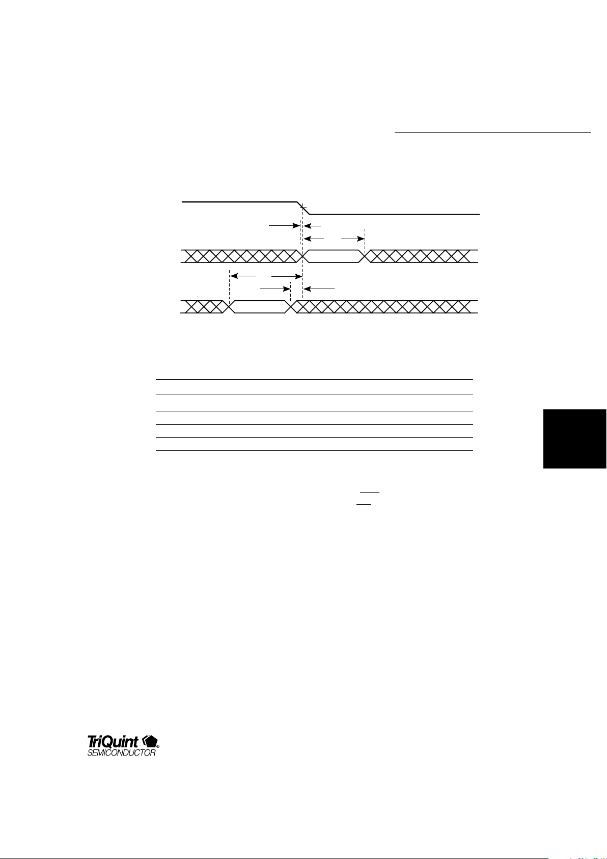
Figure 7. TQ6122 Data and Control Timing
Symbol Description Typical @ 25 °C Unit
T
DS
Data setup time
(1)
0␣ps
TDHData hold time
(2)
+325 ␣ ps
T
SS
SELA setup time
(1,3)
+350 ␣ ps
T
SH
SELA hold time
(2,3)
–100 ␣ ps
Notes: 1. Setup time is defined to be positive for data or control transitions occurring before the negative-going edge of the clock.
2. Hold time is defined to be positive for data or control transitions occurring
after the negative-going edge of the clock.
3. While SELA does not strictly have a setup and hold time, it is convenient to express its allowed transition
region limits in these terms.
SS
T
SELA
DATA
CLOCK
SH
T
DH
T
DS
T
Page 8

TQ6122
8
For additional information and latest specifications, see our website: www.triquint.com
Mechanical Characteristics
The TQ6122 DAC is packaged in a proprietary 44-pin
multilayer ceramic package which provides high-speed,
controlled-impedance interconnects and integral power
supply bypassing. The leads are set on 0.050” centers,
and are formed for gull-wing surface mounting. Figure
8 shows the pinout diagram of the packaged IC as seen
from the top, opposite the cavity side; Figure 9 lists pin
numbers, names and I/O levels. Figure 10 illustrates
the pertinent dimensions of the package and Figure 11
shows the mounting footprint.
Since the TQ6122 dissipates on the order of 1.3 W,
adequate heat sinking is essential for proper operation
of the device. Figure 12 shows one possible heat sink
arrangement based on a multi-finned “Top Hat” heat
sink available from Thermalloy. An environment with a
minimum of 100 fpm (feet per minute) of forced air
cooling is assumed; >200 fpm is preferred.
Figure 8. TQ6122 Pinout
23
12
11
34
PIN 1
VAA
IREF
ECL REF
A0
A1
DGND
A2
A3
A4
A5
VSS
VSS
CLOCK
CLOCK
N/C
SELA
DGND
BLANK
B7
B6
B5
VSS
TQ6122AM
TOP VIEW
OF MLC-44 PACKAGE
AS IT SITS ON
CIRCUIT BOARD
(CAVITY IS DOWN)
VAA
VREF
VSENSE
BLANK DISABLE
AGND
VOUT
VOUT
AGND
AGND
AGND
VSS
VSS
A6
A7
DGND
B0
B1
DGND
B2
B3
B4
VSS
Notes: 1. A7, B7 = MSB inputs
2. N/C = no internal connection
Pin Signal Interface Level (Typ.)
1, 11, 12, V
SS
–5 V
33, 34, 44
2 B5 600 mV pk–pk centered at –1.3 V @ DC
3 B6 600 mV pk–pk centered at –1.3 V @ DC
4 B7 (MSB) 600 mV pk–pk centered at –1.3 V @ DC
5 BLANK 600 mV pk–pk centered at –1.3 V @ DC
6, 28, D
GND
0 V
37, 40
7 SELA 600 mV pk–pk centered at –1.3 V @ DC
8 — No connection
9 CLOCK 1V pk–pk centered at –1.3 V @ AC
10 CLOCK 1V pk–pk centered at –1.3 V @ AC
13–15, 18 A
GND
0 V
16 V
OUT
0 V to –1 V
17 V
OUT
–1 V to 0 V
19 BLANK Enable = V
AA (IBLANK
= ON)
DISABLE Disable = A
GND (IBLANK
= OFF)
20 V
SENSE
VAA + 0.8, for VFS = 1 V pk–pk
Figure 9. TQ6122 Pin Descriptions
Pin Signal Interface Level (Typ.)
21 V
REF
VAA +1, for VFS = 1V pk–pk
22, 23 V
AA
–5 V
24 I
REF
2.5 mA for VFS = 1V pk–pk
25 ECL REF –1.3 V
26 A0 (LSB) 600 mV pk–pk centered at –1.3 V @ DC
27 A1 600 mV pk–pk centered at –1.3 V @ DC
29 A2 600 mV pk–pk centered at –1.3 V @ DC
30 A3 600 mV pk–pk centered at –1.3 V @ DC
31 A4 600 mV pk–pk centered at –1.3 V @ DC
32 A5 600 mV pk–pk centered at –1.3 V @ DC
35 A6 600 mV pk–pk centered at –1.3 V @ DC
36 A7 (MSB) 600 mV pk–pk centered at –1.3 V @ DC
38 B0 (LSB) 600 mV pk–pk centered at –1.3 V @ DC
39 B1 600 mV pk–pk centered at –1.3 V @ DC
41 B2 600 mV pk–pk centered at –1.3 V @ DC
42 B3 600 mV pk–pk centered at –1.3 V @ DC
43 B4 600 mV pk–pk centered at –1.3 V @ DC
Page 9

TQ6122
9
For additional information and latest specifications, see our website: www.triquint.com
MIXED SIGNAL
PRODUCTS
0.65
SQUARE
0.015
0.060
0.125
0.805
NOMINAL
0.005
TOP VIEW
PIN 12
0.035
All Dimensions in Inches
PIN 1
0.050
Figure 11. Mounting Footprint
Figure 10. Package Dimensions
Package Outline
(For Reference Only)
PIN 12
PIN 23
0.350
0.425
All Dimensions in Inches
PIN 34
SOLDER PAD
0.050
0.025
PIN 1
Figure 12. Heat-Sink Mounting Arrangement (heat sink not included)
THERMALLOY TYPE 2291C TOP
THERMALLOY
TYPE 2291C
BASE
THERMAL
ADHESIVE
DAC IC
Use Loctite “Output” Thermal
Conductive Adhesive (Loctite item
number 00241) or equivalent to
attach heat sink base to IC.
Page 10

TQ6122
10
For additional information and latest specifications, see our website: www.triquint.com
Circuit Description
The TQ6122 DAC is based on a current-steering architecture in which weighted currents are switched by an
array of differential-pair switches into either the V
OUT
or V
OUT
output, depending on the state of the input data
and blanking bits. Essentially, the DAC is comprised
of
six circuit blocks: the input buffer, the data multiplexer,
blanking logic, master/slave latch array with segment
encode logic, differential-pair switches, and the current
source array. (See figure on page 1.)
Input Buffers
The input buffers compare the ECL data and control
input signals with the ECLREF level, amplify the difference, and translate this signal to the logic levels used
within the IC. By default, the ECL reference is set by an
internal generator; however, for best performance and
maximum noise margin over temperature, power supply,
and device-to-device variations, the user should
provide
an external level. For general-purpose applications, a
simple resistive divider between D
GND
and VTT will
suffice. For extreme environments or for maximum
performance, the ECLREF level should be slaved to the
centerpoint of the incoming data. Refer to the “Digital
Inputs and Terminations” discussion later in this
document for additional information.
Note that the data inputs are complemented to indicate
that an increasing input value results in the V
OUT
level
moving more negative.
Data Multiplexer
The DAC makes provision for accepting data from
either of two sources: from a single 8-bit-wide word at
the full conversion rate, or from two 8-bit-wide halfspeed words which are multiplexed together inside the
DAC under the control of the SELA input. In use, the
SELA input is set HIGH to select the A-Word data and
LOW to select the B-Word. It is generally best to use
the A-Word input when operating the DAC unmultiplexed,
although the B-Word supports full-rate transfers.
Blanking Logic
A separate BLANK input is included to allow the DAC to
be used in video display applications. When asserted
LOW, the BLANK input has no effect on the operation of
the DAC, and the state of the input data words controls
the positions of the current switches. When BLANK is
asserted HIGH, however, all internal data bits and the
internal blanking bit are synchronously forced HIGH at
the next negative-going clock transition, causing the
V
OUT
output to go to its most negative level. This level
is the sum of the normal level associated with an input
code of 11111111 plus the increment due to the
blanking current being steered away from the V
OUT
output to V
OUT
. See Figure 4 (B).
In order to provide more latitude in the timing of the
BLANK signal, the BLANK input is sampled only when
the A-Word is selected. When the B-Word is selected,
the state of the BLANK input at the time the SELA
control line goes LOW is held stable until SELA again
goes HIGH. In situations where blanking is not used,
it is important that the BLANK input be tied to a solid
logic LOW to prevent accidental assertion of BLANK =
HIGH. Note also that when the DAC is used in the
unmultiplexed mode, the data should be brought in on
the A-Word inputs, since with SELA = LOW (as would
be the case for B-Word operation), a transient HIGH
level at the BLANK input would never be cleared and
the DAC would lock up.
The BLANK_DISABLE pin is normally tied to the V
AA
rail, allowing I
BLANK
to flow to the differential-pair
switch and then to the selected output. For applications
which do not use blanking, however, the standing
offset in the V
OUT
output due to the unswitched
Page 11

TQ6122
11
For additional information and latest specifications, see our website: www.triquint.com
MIXED SIGNAL
PRODUCTS
blanking current would be undesirable. For cases such
as these, the blanking current may be completely
turned off by connecting the BLANK_DISABLE pin to
A
GND
.
Master/Slave Latch With Encode Logic
A nine-wide master latch registers the data coming from
the multiplexer and blanking logic. The latch outputs
are
then split into two groups. The top three bits are translated into a seven-level thermometer code by a binaryto-N-of-seven encoder, while the lower five data bits
and the blanking bit are simply delayed. The seven
encoder outputs and the six delayed data and blanking
bits are re-registered in a slave latch to minimize skew,
which, in turn, reduces the glitch impulse. Latch timing
is set up such that the slave latch is in the “sample” mode
when the input clock is LOW, meaning that the
analog
output is updated at the falling edge of the clock.
Current Switches
The thermometer code outputs of the slave latch array
drive seven switches, each of which steers a current
equal to 1/8 of the full-scale step amplitude. The five
encoded data bits, on the other hand, switch currents
with effective binary weightings from 1/16 of full scale
down to 1/128 of full scale. The blanking bit steers a
current which is nominally 10.4% of the full-scale
amplitude.
Current-Source Array
The current-source array is the heart of the DAC from
an analog standpoint, and is responsible for generating
the segment, bit, and blanking currents. The maximum
full-scale current I
FS
(less I
BLANK
) is about 45 mA,
providing a 1.125 volt maximum swing into the 50ohm external load. The blanking current is nominally
10.4% of I
FS
, corresponding to a 10-unit IRE blanking
interval of 71 mV when the full-scale output is set to
0.679 volt. The I
REF
current tracks IFS, with a nominal
value of 2.5 mA for I
FS
= 40 mA (i.e., 6.25% of IFS).
Figure 13 (A) illustrates the basic circuit of the currentsource array, which consists of a set of current sources
ranging from the 5 mA segment currents to the binaryweighted current sources for the lower-order bits. The
circuit design utilizes source degeneration, averaging,
and linear gradient cancellation techniques to obtain
matching consistent with up to 10-bit linearity.
+
–
V
OUT
V
OUT
BLANK
DIFF-PAIR SWITCH
(TYPICAL, 15 PLACES)
I
REF
I
BLANK
I
SEG 1
I
SEG 7
I
B4
I
B3
I
B0
CASCODES
2.5 mA
(NOM)
V
REF
V
SENSE
0.8 V NOM,
FOR 1 V F.S. OUT
EXT
REF.
– 5V
V
AA
2W
3.56W
4W
4W
2W
W
RS
RS
RS
2RS
1.77
2
RS
2
V
BIAS
(INTERNAL)
BLANK
RS
RLSB
Figure 13 (A). Current-Source Array Circuit — V
SENSE
-Based Control Method
Page 12
TQ6122
12
For additional information and latest specifications, see our website: www.triquint.com
The absolute value of the current-source array output is
determined using an off-chip (silicon) reference
generator and op amp in a feedback-loop arrangement.
In Figure 13 (A), the drop across the source
degeneration resistors is compared with the level set
by the external reference. Under conditions of 1 V
peak-to-peak full-scale output swing, the voltage
between the V
SENSE
and VAA pins of the DAC will be in
the range of 0.8 V to 1.1 V, with V
REF
being in the range
of 0.7 V to 1.4 V (i.e., V
REF
may lie above or below
V
SENSE
by several hundred millivolts). Note that, for this
control method, the I
REF
terminal must be connected to
ground.
An alternative means of controlling the current-source
array output is shown in Figure 13(B), with the
advantage that now the reference current is being
sensed
after
flowing through a path identical to that of
the bit and segment currents. Thus, any error which
may have occurred due to leakage will be directly
corrected. Here, the V
SENSE
pin is left disconnected and
the I
REF
current flows to ground through a stable
resistor. The value of the resistor should be chosen to
drop about 1 volt under the desired operating
conditions, but under no circumstances should the
voltage at the I
REF
pin be allowed to drop below
–1.5 V, or the linear relationship between I
REF
and I
FS
will be degraded.
The primary limitation on the maximum output current
is the adjustment range of V
SENSE
: if the value of
{V
SENSE
– VAA} exceeds about 1.2 V, the bottom currentsource FETs begin to lose “headroom” by running up
against the sources of the cascode transistors, causing
the total current to begin limiting, as well as degrading,
the linearity. If the designer is willing to accept
somewhat degraded linearity and/or slightly higher
power dissipation, V
AA
may be taken down to –6 volts
or so, allowing V
REF
to be adjusted to give {V
SENSE
–
V
AA
} a maximum value of about 1.5 V. This translates to
an output current of about 50 mA or 1.25 V peak-topeak into the load. Note that under these conditions,
the device will not sustain any damage, but full-spec
operation of the DAC is not guaranteed.
Figure 13 (B). Current-Source Array Circuit — I
REF
-Based Control Method
+
–
V
OUT
V
OUT
BLANK
I
REF
I
BLANK
2.5 mA
(NOM)
V
REF
V
SENSE
< 1.5 V
EXT
REF.
– 5V
V
AA
V
BIAS
(INTERNAL)
BLANK
(N/C)
Page 13

TQ6122
13
For additional information and latest specifications, see our website: www.triquint.com
MIXED SIGNAL
PRODUCTS
Figure 14. Basic DAC Setup
Notes: 1. All resistors to VTT are 50-ohm, 1/8 Watt, surface-mount, mounted as close to the IC as possible.
2. All V
SS
and VTT capacitors are rated ≥15 V. All VAA capacitors are rated ≥ 25 V.
3. Use either surface-mount components or keep minimum-length leads on all resistors and capacitors.
4. For best noise isolation, the analog supply (V
AA
) and digital supply (VSS) should connect at
only one point, via decoupling networks such as ferrite beads.
5. The input circuitry for B0–B7, BLANK, and SELA are the same as for A0–A7.
6. For questions regarding board layout, please contact the factory.
IREF
VAA
VREF
VSENSE
BLK.DIS.
AGND
VOUT
VOUT
AGND
AGND
DGND
VSS
1uF
1µF
V PLANE
50
A5
A4
A3
A2
A1
A0
EXT.
ECL
REF.
DGND
ECL
REF.
1µF
.01µF
1000 pF
50
SELA
BLANK
CLK
CLK
1000
pF
B5
B6
B7
+
–
MC1403A
V PLANE
V
V (V + 2.5 V)
MC33071
1uF
2.5 K
V
V
620
(V +1 V)
V
V
V
(I = ON)
(I = OFF)
Z = 50
Short microstrip or
buried stripline
+ –
1 K Adjust for desired
full-scale output
VSS
DGND
DGND
VSS
VSS
DGND
DGND
NOTE 5
A6
A7
B0
B1
B2
B3
B4
50
NOTE 5
NOTE 5
u = Microstrip or other
transmission line
u
u
u
u
u
u
uuuu
uu
u
u
u
u
u
u
u
u
NOTE 5
V
AA
V
AA
O
OUT
OUT
BLANK
BLANK
CC
EE
2.5 K
AA
AA
AA
AAOUT
1 K
AA
Split power supply planes here to minimize noise
coupling into analog circuitry.
Use a common plane for analog and digital grounds.
SS
V PLANE
SS
V PLANE
SS
V PLANE
AA
L
1
L
2
-5 V
SUPPLY
L , L = Fair-Rite 2743001111
1
2
V = -5 +0.5 V
SS
V = -5 +0.25 V
AA
A7, B7 = MSB
V PLANE
SS
V PLANE
TT
V = -2 V
TT
V PLANE
TT
V PLANE
TT
1000 pF
.01µF
1000 pF
.01µF
.01µF
1000 pF
1000 pF
.01µF
.01µF
.01µF
1000 pF
Application Information
Figure 14 illustrates the basic connection of the DAC,
showing details for power supplies, data and clock
inputs, and outputs terminated in 50-ohm transmission
line loads. Some issues relating to circuit board layout
are also addressed.
Page 14

TQ6122
14
For additional information and latest specifications, see our website: www.triquint.com
Power Supplies, Ground and Bypassing
To minimize noise coupling, the digital and analog
power supplies should be returned to a single-point
ground, and power supply buses to the IC should have
minimum impedance (power planes are best).
The supplies themselves should be well bypassed at high
and low frequencies, which requires the use of several
different parallel capacitors as shown. The values are not
particularly critical; however, due to the fact that a
capacitor looks inductive above its self-resonant
frequency, one needs to use several different values in
parallel, ranging from microfarads to nanofarads, in
order to provide adequate wideband bypassing.
For best results, use leadless ceramic chip capacitors
for bypassing, although leaded components will work
satisfactorily if higher noise can be tolerated. A common
ground plane has been found to give the best performance.
For best results and minimum noise, the digital and
analog supplies should be physically separated on the
circuit board. When using a common –5␣ V feed, the
V
SS
and VAA planes should be isolated by ferrite beads
(Fair-Rite P/N 2743001111 or equivalent) as shown in
Figure 14. Using separate LM337MT regulators downstream of the ferrite beads will provide better isolation.
Digital Inputs and Terminations
The TQ6122 DAC is designed to accept ECL logic levels
at all data and control inputs. All ECL inputs, with the
exception of the clock (see below), are single-ended
and are compared to the ECL threshold reference of
–1.3␣ Volts (nominal) in the input buffers of the DAC.
The ECL reference input equivalent circuit is shown in
Figure 1. Several options are available to the user for
externally setting the ECL reference level. The simplest
option is that of a voltage divider between D
GND
and
V
TT
, setting the ECL termination voltage as shown in
Figure␣ 15 (A). The nominal value for ECLREF is –1.3␣ V;
however, due to input offset variations among the input
buffers or variations in V
TT
, some adjustment above or
below –1.3 V may give the best results.
A good way to settle ECLREF is to slave the ECL reference level to the center (switching) point of the input
data signal. This may be accomplished in two ways:
either use the V
BB
generator output of the device which
is generating the ECL signals supplied to the DAC, or
use an inverter with input and output connected
together to generate a level equal to the switching
threshold. See Figure␣ 15 (B). Note that the ECLREF
generator should be able to source and sink up to
approximately 5␣ mA, since the input resistance is about
50␣ ohms, against an internal –1.3␣ V (nominal) voltage
source. An additional op amp may be used to give
more flexibility or more robust drive. See Figure␣ 15 (C).
Figure 15. External ECL Reference Generator
(A) (B) (C)
200
50
V
ECL Reference
input or unused
clock (CLK) input
EXTERNAL ECL
INVERTER
50
(OPTIONAL OP AMP)
DAC
INPUT
ECLREF
–
+
TT
-2 V
V
TT
-2 V
Page 15

TQ6122
15
For additional information and latest specifications, see our website: www.triquint.com
MIXED SIGNAL
PRODUCTS
Clock Input
In order to realize the full speed potential of the DAC, a
clock with an input swing of at least 1 V peak-to-peak,
nominally centered on –1.3 V, is required. The clock
may be applied in either single-ended or differential
fashion. Because a differential clock provides maximum
speed and best control of the relationship between clock
and output transitions, as well as minimum noise,
it is
the preferred solution. For single-ended clock drive, the
customer must drive the unused CLOCK input with an
external ECL reference level, which may be generated
using a resistive divider or, for best results, an external
inverter tied back on itself. See Figure 15.
Input Line Termination
As shown in Figure 14, data, control, and clock inputs
should be terminated in 50 ohms to V
TT
, consistent
with good ECL practice. For best results, keep
terminations physically small — surface-mount “chip”
resistors work very well — and locate them as close to
the IC as possible. The V
TT
bus should also be locally
bypassed to digital ground, using chip capacitors
placed close to the terminations. The DAC offers good
performance for –2.5 V
< VTT < –2 V, where the use of
V
TT
< –2 V may allow the designer to eke out the last
bit of performance in a noisy or marginal drive-level
environment.
Current-Source Control Loop
As illustrated previously in Figure 13, and shown in
detail in Figure 16, the bit current sources are
controlled by placing them in a feedback loop which
compares the drop across a current-sensing resistor
with a stable reference. For nominal 1 Volt full-scale
output swing, the V
REF
-to-VAA voltage will be in the 0.8
to 1 V range, and may be derived from a zener or,
better still, a bandgap reference such as the 2.5 V
Motorola MC1403A. The output of the bandgap
reference will have to be divided down before being
applied to the control op amp, and some means should
be provided to trim the output to compensate for V
OUT
load resistor variations.
The op amp must have input common-mode and
output drive ranges which extend down to within at
least 0.5 Volt of the negative rail for maximum control
range. For best noise immunity, both the reference
generator and the op amp should share a point
connection to the V
AA
rail, close to the DAC. The
Motorola MC33071 op amp is suitable for this
application. Standard linear design techniques should
be used to minimize thermal drift and offset. Note that
the temperature coefficient of the nichrome resistors
used in the DAC is on the order of +6 ppm/°C. Figure 16
shows a typical reference control loop circuit.
IREF
VAA
VREF
VSENSE
BLK.DIS.
AGND
VOUT
VOUT
AGND
AGND
DGND
+
–
MC1403A
V PLANE
V
V (V + 2.5 V)
MC33071
1uF
0.01
1000
2.5 K
V
V
620
(V +1 V)
V
+ –
1 K
V
AA
CC
EE
2.5 K
AA
AA
AA
AAOUT
1 K
AA
(I = ON)
(I = OFF)
V
AA
BLANK
BLANK
V
V
OUT
OUT
Fig. 16. Typical External Current-Source Control Loop
Figure 17 illustrates the relationship between control
input V
REF
and the full-scale output swing. Note that the
full-scale swing may be reduced below 0.25 V peak-topeak by pulling V
REF
below VAA. However, this
necessitates a separate negative supply for the control
Page 16

TQ6122
16
For additional information and latest specifications, see our website: www.triquint.com
op amp and reference generator, which may decrease
the V
AA
supply rejection. In circuits which use different
negative rails for the DAC V
AA
supply and the op amp,
V
REF
should be clamped to no more than two diode
drops below V
AA
, and a current-limiting resistor should
be included at either the op amp output or between its
negative supply input and supply input. In the event of
turn-on transients and large excursions in the op amp
supply before V
AA
has settled out, these precautions
will help prevent breakdown of circuitry within the DAC.
Figure 17. Typical V
REF
-to-VAA Transfer Characteristics
1.25
1.125
1.00
0.75
0.50
-1.0 0 0.5 1.0 1.25
V
OUT
(Volts p-p)
(Maximum recommended)
0.25
V to V
(Volts)
REF
AA
Full-Scale Output Adjust
The procedure for setting the full-scale output range is
quite straightforward, and involves monitoring the
output level(s) using a DVM. With the DAC connected
to its actual V
OUT
and V
OUT
load(s), the output is
alternately switched between steady state zero- and
full-scale levels, and the reference is adjusted until the
desired full-scale transition amplitude is obtained. The
clock must be running and the BLANK input set to “0”.
Alternatively, for a DDS application, a spectrum
analyzer or a power meter may be used to monitor the
full-scale output power.
Blanking Current Programming
The blanking current (I
BLANK
in Figure 13) is turned off
by connecting the BLANK_DISABLE pin to A
GND
to
divert the current away from the blank switch and the
output of the DAC, and turned on by connecting
BLANK_DISABLE to V
AA
.
Output Equivalent Circuit
Figure 5 illustrates the equivalent circuit of the two DAC
outputs. Each of the bit current sources is switched
into either the V
OUT
or the V
OUT
output, depending on
the data stored in the slave latches. A pair of internal
50-ohm resistors are connected from V
OUT
and V
OUT
to
analog ground (A
GND
), and provide reverse termination
for the analog output transmission lines. Although in
principle there is no restriction on the load impedance
applied at the outputs, in practice, the best
performance will be obtained when driving a 50-ohm
terminated transmission line. This is very important
from a settling standpoint, since reflections from non50-ohm loads will superimpose with new transitions
and interfere with settling. The general rule for
terminating the outputs is “the cleaner, the better.”
Output Zero-Scale Adjust
The output baseline, or “zero-scale” level, may be
adjusted by returning the far-end termination resistors
to a well-bypassed supply level other than ground. For
this general situation, reference Figure 5, the instantaneous output voltages V
OUT
and V
OUT
are given by:
) –
|
I
OUT
| (RL1 || RT1)
) –
|
I
OUT
| (RL2 || RT2)
V
OUT
= V
OS
(
RL1 + R
T1
R
T1
V
OUT
= V
OS
(
RL2 + R
T2
R
T2
I
OUT =
(
Digital Input
255
) I
FS
I
OUT =
(1 –
Digital Input
255
) I
FS
IFS = Summation of all individual bit currents
Digital Input = Decimal equivalent of the binary input word
Page 17

TQ6122
17
For additional information and latest specifications, see our website: www.triquint.com
MIXED SIGNAL
PRODUCTS
disadvantage of requiring a large supply voltage. In
general, a 1/8 to 1/4 W carbon-composition resistor
with a value of 500 to 1000 ohms will give good
performance. Keep the lead lengths short when attaching to the circuit board and bypass the driven terminal
of the resistors with a 1000 pF to 0.01 µF SMT (surfacemount) capacitor network to the ground plane.
A transistor current source, on the other hand, requires
much less power supply overhead, but adds more
capacitance to the transmission line. If a transistor is
used, it should be a high-F
T
device with low CCB or C
DG
(≤ 0.5 pF, if possible) and installed with short leads.
Capacitive coupling provides a means of obtaining an
output centered on 0 volts. However, simply adding a
coupling capacitor at one (or both) of the outputs will
cause the DC output level to exceed the –1.5 V output
compliance limit. The way to circumvent this problem
is to add an offset current between the DAC output and
the coupling capacitor (as discussed above), or to add
a low-loss 50-ohm pad between the DAC and the
capacitor, as shown in Figure 18(B). A “T” or “π”
attenuator topology is acceptable, having 1␣ dB to 3 dB
of attenuation. The characteristic impedance must be
consistent with the overall system impedance, typically
50 ohms. This approach works, although the lower
limit on the output level tends to be very close to the
–1.5 V compliance limit for ≥1 V full-scale output
swings, so some care and verification will be required.
DAC
0 VOLT
V
0 VOLT
50
MIMIMUM-LOSS PAD (1–3 dB)
MIN
Figure 18(B). AC Coupling of Outputs
Figure 18(A). Alternate Output Offset Current Generators
For the case of RL1 = RL2 = RT1 = RT2 = 50 ohms, VOS is
attenuated by 50%. An overriding factor in setting the
output offset is the requirement that V
OUT
and V
OUT
always remain within the device’s output compliance
range of –1.5 V to +1 V. Note also that in the case of
the video application of the DAC, the value of the
blanking current I
BLANK
and the state of the BLANK
input must be included in the expressions for V
OUT
and
V
OUT
.
An alternative method of offsetting the output involves
injecting an offset current at the output. This may be
done using a current source in the form of either a
resistor or a transistor as shown in Figure 18(A). The
resistor has the advantage of minimizing perturbation
of the transmission line impedance, with the
V
OS
1000 pF
0.01 uF
500 – 1 K
1/8 – 1/4W
Carbon Comp.
50 Ohm
R
1
R
2
R
3
V
T
50 Ohm
R
E
High-F
Low C
Device
JE
T
Short
Lead
Short
Lead
Note: V
MIN
must not exceed the lower output
compliance limit of –1.5 V for proper
operation. If V
MIN
< –1.5 V, decrease
the DAC output swing by adjusting the
V
REF
drive to the control op amp.
Page 18

TQ6122
18
For additional information and latest specifications, see our website: www.triquint.com
Figures 19 through 23 show typical AC performance
of the TQ6122. Figures␣ 19A and 19B illustrate the
response of the DAC to an unmultiplexed counter
input at 1 Gs/s and 1.5␣ Gs/s, respectively.
Blanking is enabled in both cases.
The small glitches appearing at 1/8 of full-scale
intervals are shown in more detail in Figure 22.
Figure 19 (A). Unmuxed Ramp at 1000 Ms/s with
Blanking (Guaranteed, 0 to +85
°
C)
Figure 19(B). Unmuxed Ramp at 1500 Ms/s with
Blanking (Typical, +25
°
C)
Typical AC Performance
Page 19

TQ6122
19
For additional information and latest specifications, see our website: www.triquint.com
MIXED SIGNAL
PRODUCTS
Figure 20(A). Muxed Ramp at 1000 Ms/s with Blanking
Multiplexed behavior is shown in Figure 20A and 20B,
with a counter input muxed against fixed levels at
1000 Ms/s and at 1350 Ms/s, respectively.
In Figure 20A, the ramp is muxed against a steady
state mid-scale value, while in Figure 20B, the steady
state input is 11111111. The apparent droop in the top
level in Figure 20B is an artifact of the sampler.
Figures 19A, 19B, and 20A show the effects of blanking,
while in Figure 20B, the BLANK input is held LOW,
demonstrating the repetitive nature of the waveform.
Figure 20(B). Muxed Ramp at 1350 Ms/s with
Blanking Disabled
Note: In Figure 20(A), A0–A7 are switched, B0–B6 are LOW,
B7is HIGH and BLANK is switched. In Figure 20(B),
A0–A7 are switched, B0–B7 are HIGH, and BLANK is LOW.
Page 20

TQ6122
20
For additional information and latest specifications, see our website: www.triquint.com
Figure 21. Typical Full-Scale Transitions
at V
OUT
and V
OUT (fCLK
= 1000 MHz)
Figure 22. Typical Worst-Case Glitch Impulse
(f
CLK
= 1000 MHz)
Figure 21 illustrates the symmetry of complementary
full-scale transitions at V
OUT
and V
OUT
, while Figure 22
depicts a typical worst-case glitch of 6 pV/sec.
Page 21

TQ6122
21
For additional information and latest specifications, see our website: www.triquint.com
MIXED SIGNAL
PRODUCTS
Figure 23(A). Synthesized Sine Wave Output
Figure 23(A) shows a 1 Gs/s, 58.6 MHz sine wave, and
Figure 23B shows its corresponding spectrum. The
spurious-free dynamic range is 46␣ dBc, a typical value
for the device.
In Figure 23(B), the DAC output is attenuated by 6 dB
going into a spectrum analyzer.
Figure 23(B). Spectrum of a 58.5 MHz Sine Wave
at 1 Gs/s
Page 22

TQ6122
22
For additional information and latest specifications, see our website: www.triquint.com
Figure 25. Chip Dimensions, Topography, and Padout
Notes: 1. Dimensional limits unless otherwise
specified:
+2 mils (+51 µM).
2. Pins labeled N/C are not
connected internally.
Figure 24. Complex Modulated Sine Wave Pattern
at 1000 Mb/s
Figure 24 shows a modulated sine wave as an example
of a more complex waveform.
VAA
VAA
IREF
ECL REF
A0 (LSB)
A1
DGND
DGND
DGND
A2
A3
A4
A5
VSS
VSS
VSS
VSS
CLOCK
CLOCK
N/C
SELA
DGND
DGND
DGND
BLANK
B7 (MSB)
B6
B5
VSS
VSS
VAA
VAA
VREF
VSENSE
BLANK DISABLE
AGND
AGND
AGND
AGND
VOUT
VOUT
VOUT
AGND
AGND
VSS
VSS
VSS
A6
A7 (MSB)
DGND
DGND
B0 (LSB)
B1
DGND
DGND
B2
B3
B4
VSS
VSS
VOUT
DIE SIZE: 129 Mils x 111 Mils (3110 µM x 2660 µM)
Page 23

TQ6122
23
For additional information and latest specifications, see our website: www.triquint.com
MIXED SIGNAL
PRODUCTS
Ordering Information
TQ6122-M
8-bit, 1 Gs/s DAC in 44-pin package
TQ6122-D
8-bit, 1 Gs/s DAC, die only
ETF6122
Engineering Test Fixture with 6122 device
Additional Information
For latest specifications, additional product information,
worldwide sales and distribution locations, and information about TriQuint:
Web: www.triquint.com Tel: (503) 615-9000
Email: sales@tqs.com Fax: (503) 615-8900
For technical questions and additional information on specific applications:
Email: applications@tqs.com
The information provided herein is believed to be reliable; TriQuint assumes no liability for inaccuracies or
omissions. TriQuint assumes no responsibility for the use of this information, and all such information
shall be entirely at the user's own risk. Prices and specifications are subject to change without notice.
No patent rights or licenses to any of the circuits described herein are implied or granted to any third party.
TriQuint does not authorize or warrant any TriQuint product for use in life-support devices and/or systems.
Copyright © 1997 TriQuint Semiconductor, Inc. All rights reserved.
Revision 1.0.A October 1997
Figure 26. Package Labelling (44-pin packaged version)
See Figures 10, 11 and 12 for package dimensions and heat-sink mounting information.
1 TQS USA
TQ6122-M
YYWW XXXX
BEVELED
CORNER
Component Material
Lead Kovar
Lead Plating Lead/tin alloy
YYWW – Date Code
XXXX - Lot Number
 Loading...