

Page 1
WIRELESS COMMUNICATIONS DIVISION
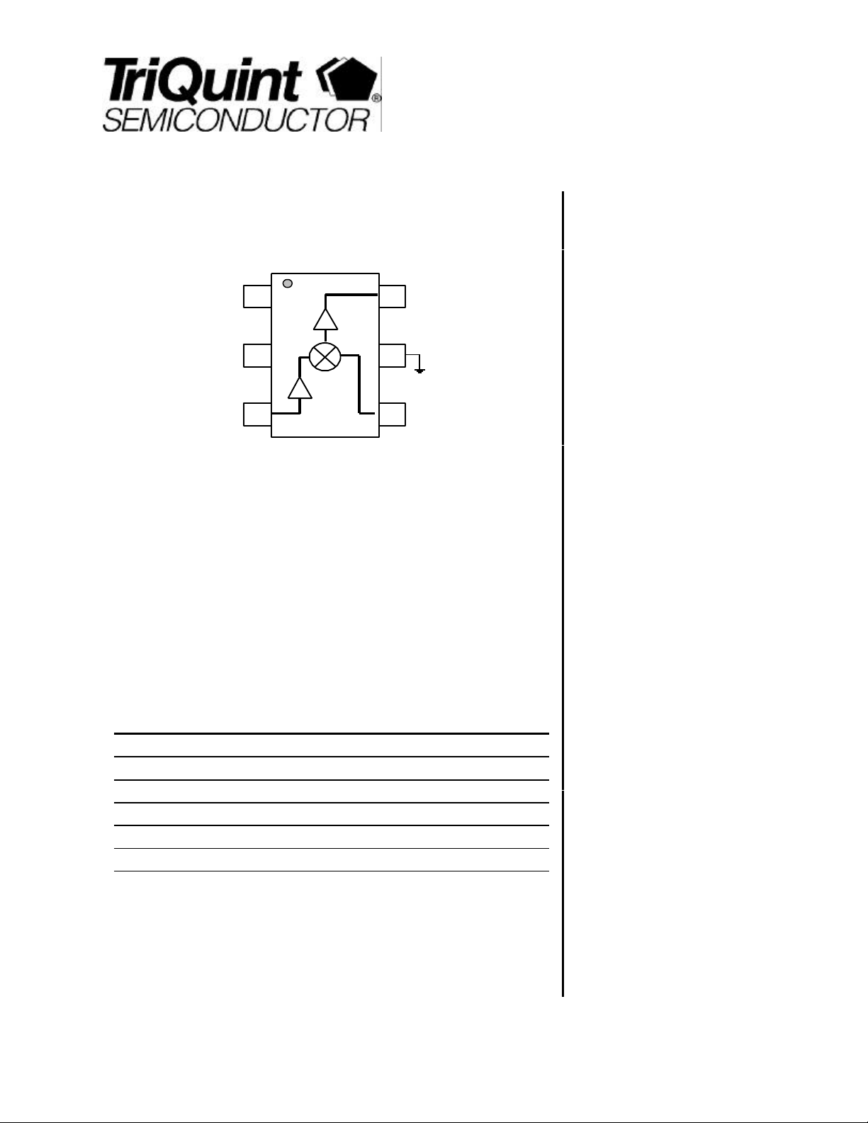
TQ5M31
Vdd
Gain/IP3/current
adjustment
Vdd
GIC
IF
OUT
GND
IF
DATA SHEET
3V Downconverter
Mixer IC
GND
50 ohm
LO INPUT
LO
RF
50 ohm
RF INPUT
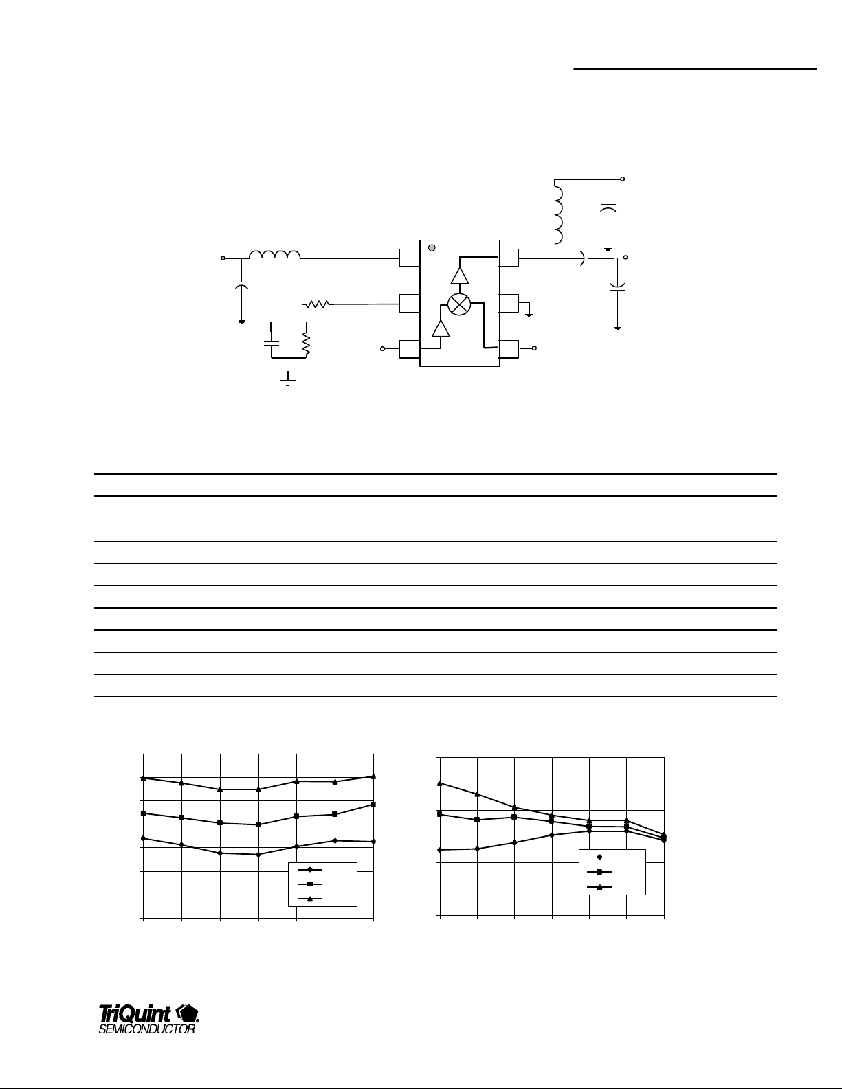
Product Description
The TQ5M31 is a general purpose RFIC mixer downconverter designed for multiple
applications including worldwide cellular and PCS mobile phones, ISM bands, GPS
receivers, L band satellite terminals, WLAN and pagers. The TQ5M31 is usable for
applications with an RF frequency range from 500 to 2500 MHz, and an IF output
range from 45 to 500 MHz. The integrated circuit requires minimal off-chip
matching, while allowing for the maximum application flexibility. Low current drain
makes this part ideal for portable, battery operated applications. The output third
order intercept efficiency is very high.
Electrical Specifications
Parameter Min Typ Max Units
RF Frequency 500 2500 MHz
Conversion Gain 4.0 dB
Noise Figure 8.5 dB
Input 3rd Order Intercept 9.0 dBm
DC supply Current 6.2 mA
Note 1: Test Conditions: Vdd=2.8V, Ta=25C, RF=1960MHz, LO=1750MHz, IF=210MHz, LO input=-
4dBm
1
Features
§ Single 3V Operation
§ Adjustable Gain/IP3/Current
§ Low Current Operation
§ Few external components
§ SOT23-6 plastic package
§ High IP3
§ Broadband Performance
Applications
§ Cellular and PCS mobile applications
worldwide
§ Wireless data applications
§ GPS/ISM/ general purpose
For additional information and latest specifications, see our website: www.triquint.com 1
Page 2
TQ5M31
Data Sheet
Electrical Characteristics
Parameter Conditions Min. Typ/Nom Max. Units
RF Frequency 500 1960 2500 MHz
LO Frequency 600 1750 2700 MHz
IF Frequency 45 210 500 MHz
LO input level -7 -4 0 dBm
Supply voltage 2.7 2.8 4.0 V
Conversion Gain 3.0 4.0 dB
Input 3rd Order Intercept 6.5 9.0 dBm
Supply Current 6.2 8.5 mA
Note 1: Test Conditions (devices screened to the above test conditions): Vdd=2.8V, RF=1960MHz, LO=1750MHz, IF=210MHz, LO input=-4dBm, TC = 25° C, unless
otherwise specified.
Absolute Maximum Ratings
Parameter Value Units
DC Power Supply 5.0 V
Power Dissipation 100 mW
Operating Temperature -40 to 85 C
Storage Temperature -60 to 150 C
Signal level on inputs/outputs +20 dBm
Voltage to any non supply pin +.3 V
2 For additional information and latest specifications, see our website: www.triquint.com
Page 3
TQ5M31
Data Sheet
Cellular Band Typical Electrical Characteristics
Parameter Conditions Min. Typ/Nom Max. Units
Conversion Gain 3.5 dB
Noise Figure 9.5 dB
Input 3rd Order Intercept 9.0 dBm
Return Loss Mixer RF input
Mixer LO input
Isolation RF to IF; after IF match
LO to IF; after IF match
IF Output Impedance Mixer “On”
Mixer “Off”
Supply Current 4.5 mA
Note 1: Test Conditions: Vdd=2.8V, RF=881MHz, LO=991MHz, IF=85MHz, LO input=-4dBm, TC = 25° C, unless otherwise specified.
10
10
33
40
500
<50
dB
dB
dBm
dBm
Ω
Ω
PCS Band Typical Electrical Characteristics
Parameter Conditions Min. Typ/Nom Max. Units
Conversion Gain 4.0 dB
Noise Figure 9.5 dB
Input 3rd Order Intercept 9.0 dBm
Return Loss Mixer RF input
Mixer LO input
Isolation RF to IF; after IF match
LO to IF; after IF match
IF Output Impedance Mixer “On”
Mixer “Off”
Supply Current 6.0 mA
Note 1: Test Conditions: Vdd=2.8V, RF=1960MHz, LO=1750MHz, IF=210MHz, LO input=-4dBm, TC = 25° C, unless otherwise specified.
10
10
33
40
500
<50
dB
dB
dBm
dBm
Ω
Ω
For additional information and latest specifications, see our website: www.triquint.com 3
Page 4
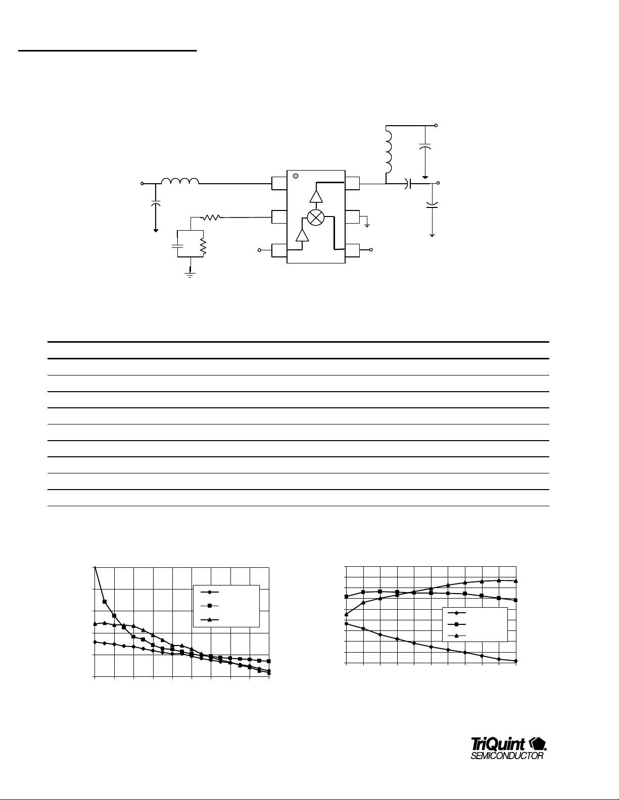
TQ5M31
Variable bypass (R4), total resistance
Data Sheet
Typical Performance/Applications circuit for GIC tuning plots
Test Conditions (Unless Otherwise Specified): Vdd=2.8V, Ta=25C, RF=1960MHz, LO=1750MHz, IF=210MHz,Current≈6mA, Gain≈4dB, IIP3≈+10dB
Vdd
C2
C3
IF
OUT
C4
Vdd
C1
L1
R3
Vdd
GIC
L2
IF
GND
50 ohm
RF
RF
INPUT
C7
R4
50 ohm LO
INPUT
LO
Bill of Material for TQ5M31 Downconverter Mixer for GIC tuning plots
Component Reference Designator Part Number Value Size Manufacturer
Receiver IC U1 TQ5M31 SOT23-6 TriQuint Semiconductor
Capacitor C1 470pF 0402
Capacitor C2 1000pF 0402
Capacitor C3 22pF 0402
Capacitor C4 27pF 0402
Capacitor C7 150 pF 0402
Inductor L1 2.2nH 0402
Inductor L2 39nH 0402
Resistor R3, R4 Select 0402
25
20
15
10
Performance
5
0
10 30 50 80 110 140 180 220 260 320
4 For additional information and latest specifications, see our website: www.triquint.com
Conversion Gain, Idd and IIP3 Vs Rbias
(Vdd = 2.8v, PLO = - 4dBm)
CG (dB)
Idd (mA)
IIP3 (dBm)
Rbias (ohms)
Performance Vs. Bypass DC Bias Resistance
(RF = 1960 MHz, Vdd = 2.8v, PLO = -4 dBm)
21
18
15
12
9
6
3
Performance
0
-3
-6
100 90 80 70 60 50 40 30 20 10 0
(R3 +R4 = 103 ohm)
Gain (dB)
OIP3 (dBm)
IIP3 (dBm)
Page 5
TQ5M31
Data Sheet
Cellular Band Typical Performance/Applications circuit
Test Conditions (Unless Otherwise Specified): Vdd=2.8V, Ta=25C, RF=881MHz, LO=966MHz, LO input –4dBm, IF=85MHz,Current≈9mA, Gain≈9dB, IIP3≈+10dB
Vdd
C2
C3
IF
OUT
C4
Vdd
C1
L1
R3
Vdd
GIC
L2
IF
GND
50 ohm
RF
RF
INPUT
C7
R4
50 ohm LO
INPUT
LO
Bill of Material for TQ5M31 Downconverter Mixer Cellular band
Component Reference Designator Part Number Value Size Manufacturer
Receiver IC U1 TQ5M31 SOT23-6 TriQuint Semiconductor
Capacitor C1 1000pF 0402
Capacitor C2 1000pF 0402
Capacitor C3 20pF 0402
Capacitor C4 22pF 0402
Capacitor C7 150pF 0402
Inductor L1 2.2nH 0402
Inductor L2 39nH 0402
Resistor R3 3.3ohm 0402
Resistor R4 39ohm 0402
Noise Figure vs. Temperature vs. Frequency
11
10
12
Input IP3 vs. Temperature vs. Frequency
9
8
7
Noise Figure (dB)
6
5
4
865 870 875 880 885 890 895
Frequency (MHz)
-40 C
+25 C
+85 C
For additional information and latest specifications, see our website: www.triquint.com 5
11
IIP3 (dBm)
10
9
865 870 875 880 885 890 895
Frequency (MHz)
-40 C
+25 C
+85 C
Page 6

TQ5M31
Data Sheet
Input IP3 vs. LO Drive vs. Frequency
13
12
11
10
9
IIP3 (dBm)
8
7
6
865 870 875 880 885 890 895
Frequency (MHz)
Idd vs. Temperature vs. Frequency
5.5
5
4.5
Idd (mA)
4
3.5
3
865 870 875 880 885 890 895
Frequency (MHz)
Idd vs. Vdd vs. Temperature
6
5.5
5
4.5
4
Idd (mA)
3.5
3
2.5
2
1.8 2.8 3.8 4.8
PLO = -7 dBm
PLO = -4 dBm
PLO = -1 dBm
-40 C
+25 C
+85 C
-40 C
+25 C
+85 C
Vdd (v)
Conversion Gain vs. Temperature vs. Frequency
5
-40 C
+25 C
4
Gain (dB)
3
2
865 870 875 880 885 890 895
Frequency (MHz)
Conversion Gain vs. LO Drive vs. Frequency
4
3
Gain (dB)
2
865 870 875 880 885 890 895
Frequency (MHz)
Conversion Gain vs. Vdd vs. Frequency
5
4
3
Gain (dB)
2
1
865 870 875 880 885 890 895
Frequency (MHz)
+85 C
PLO = -7 dBm
PLO = -4 dBm
PLO = -1 dBm
1.8 v
2.8 v
3.8 v
4.8 v
6 For additional information and latest specifications, see our website: www.triquint.com
Page 7

TQ5M31
Data Sheet
PCS Band Typical Performance/Applications circuit
Test Conditions (Unless Otherwise Specified): Vdd=2.8V, Ta=25C, RF=1960MHz, LO=1750MHz, LO input –4dBm, IF=210MHz,Current≈6mA, Gain≈3dB, IIP3≈+10dB
Vdd
C2
C3
IF
OUT
C4
Vdd
C1
L1
R3
Vdd
GIC
L2
IF
GND
50 ohm
RF
RF
INPUT
C7
R4
50 ohm LO
INPUT
LO
Bill of Material for TQ5M31 Downconverter Mixer PCS band
Component Reference Designator Part Number Value Size Manufacturer
Receiver IC U1 TQ5M31 SOT23-6 TriQuint Semiconductor
Capacitor C1 470pF 0402
Capacitor C2 1000pF 0402
Capacitor C3 22pF 0402
Capacitor C4 27pF 0402
Capacitor C7 150pF 0402
Inductor L1 2.2nH 0402
Inductor L2 39nH 0402
Resistor R3 12ohm 0402
Resistor R4 91ohm 0402
TQ5M31 Performance
17
15
13
11
9
Performance
7
5
3
1930 1940 1950 1960 1970 1980 1990
Frequency (MHz)
IP3_out (dBm)
IP3_in (dBm)
Idd (mA)
C/G(dB)
For additional information and latest specifications, see our website: www.triquint.com 7
Conversion Gain vs. Temperature vs. Frequency
5
4
3
Gain (dB)
2
1
1930 1940 1950 1960 1970 1980 1990
Frequency (MHz)
-40 C
+25 C
+85 C
Page 8

TQ5M31
Input IP3 vs. Temperature vs. Frequency
Data Sheet
Conversion Gain vs. Vdd vs. Frequency
5
4
Gain (dB)
3
2
1940 1950 1960 1970 1980 1990
Frequency (MHz)
Conversion Gain vs. Vdd vs. Temperature
6
5
4
3
Gain (dB)
2
1
1.8 2.8 3.8 4.8
Vdd (v)
1.8 v
2.8 v
3.8 v
4.8 v
-40 C
+25 C
+85 C
Noise Figure vs. Vdd vs.Temperature
11
10
9
8
7
NF (dB)
-40 C
+25 C
+85 C
-40 C
+25 C
+85 C
6
5
4
1.8 2.8 3.8 4.8
Noise Figure vs. Temperature vs. Frequency
11
10
9
8
7
6
Noise Figure (dB)
5
4
1930 1940 1950 1960 1970 1980 1990
Vdd (v)
Frequency (MHz)
Conversion Gain vs. LO Drive Level vs. Frequency
5
4
3
Gain (dB)
2
1
1930 1940 1950 1960 1970 1980 1990
Frequency (MHz)
PLO = -7 dBm
PLO = -4 dBm
PLO = -1 dBm
13.5
13
12.5
12
11.5
11
IIP3 (dBm)
10.5
10
9.5
9
1930 1940 1950 1960 1970 1980 1990
8 For additional information and latest specifications, see our website: www.triquint.com
-40 C
+25 C
+85 C
Frequency (MHz)
Page 9

TQ5M31
Data Sheet
Input IP3 vs. LO Drive Level vs. Frequency
13
12
IIP3 (dBm)
11
10
1930 1940 1950 1960 1970 1980 1990
14
13
12
11
IIP3 (dBm)
10
9
8
1.8 2.8 3.8 4.8
Frequency (MHz)
Input IP3 vs. Vdd vs. Temperature
Vdd (v)
PLO = -1 dBm
PLO = -4 dBm
PLO = -7 dBm
-40 C
+25 C
+85 C
Idd vs. Temperature vs. Frequency
8
7
6
Idd (mA)
5
4
1930 1940 1950 1960 1970 1980 1990
Frequency (MHz)
Idd vs. Vdd vs. Temperature
8
7.5
7
6.5
Idd (mA)
6
5.5
5
1.8 2.8 3.8 4.8
Vdd (v)
-40 C
+25 C
+85 C
-40 C
+25 C
+85 C
For additional information and latest specifications, see our website: www.triquint.com 9
Page 10

TQ5M31
Data Sheet
ISM Band Typical Performance/Applications circuit
Test Conditions (Unless Otherwise Specified): Vdd=2.8V, Ta=25C, RF=2443MHz, LO=2203MHz, LO input –4dBm, IF=240MHz,Current≈7mA, Gain≈2.5dB, IIP3≈+9dB
Vdd
C2
C3
IF
OUT
C4
Vdd
C1
L1
R3
Vdd
GIC
L2
IF
GND
50 ohm
RF
RF
INPUT
C7
R4
50 ohm LO
INPUT
LO
Bill of Material for TQ5M31 Downconverter Mixer PCS band
Component Reference Designator Part Number Value Size Manufacturer
Receiver IC U1 TQ5M31 SOT23-6 TriQuint Semiconductor
Capacitor C1 220pF 0402
Capacitor C2 1000pF 0402
Capacitor C3 12pF 0402
Capacitor C4 10pF 0402
Capacitor C7 150pF 0402
Inductor L1 1.8nH 0402
Inductor L2 47nH 0402
Resistor R3 20ohm 0402
Resistor R4 47ohm 0402
ISM Band: Idd vs. Vdd vs. Frequency
8.5
8
7.5
Idd (mA)
7
Vdd=2.8V
6.5
6
2400 2420 2440 2460 2480
Vdd=1.8V
Vdd=3.8V
Vdd=4.8V
Frequency (MHz)
Converson Gian (dB)
ISM band: C/G vs. LO Drive vs. Frequency
3.5
3.3
3.1
2.9
2.7
2.5
2.3
2.1
1.9
1.7
1.5
2400 2420 2440 2460 2480
PLO=-7dBm
PLO=-4dBm
PLO=-1dBm
Frequency (MHz)
10 For additional information and latest specifications, see our website: www.triquint.com
Page 11

TQ5M31
Data Sheet
ISM Band: IIP3 vs. LO Drive Level vs. Frequency
11
10.5
10
9.5
9
IIP3 (dB)
8.5
8
7.5
7
2400 2420 2440 2460 2480
Frequency (MHz)
PLO=-1dBm
PLO=-4dBm
PLO=-7dBm
ISM Band: Conversion Gain vs. Vdd vs. Frequency
4.5
4
3.5
3
2.5
2
1.5
Conversion Gain (dB)
1
0.5
0
2400 2410 2420 2430 2440 2450 2460 2470 2480
Vdd=1.8V
Vdd=2.8V
Vdd=3.8V
Vdd=4.8V
Frequency (MHz)
For additional information and latest specifications, see our website: www.triquint.com 11
Page 12

TQ5M31
Data Sheet
General Description
TQ5M31 is a general purpose RFIC mixer downconverter
designed for multiple applications. The mixer is implemented
with a single common-source GaAs MESFET and is designed
to operate with supply voltages from 1.8 to 5 Volts. To use the
TQ5M31, tuning components must be selected for the LO
buffer amplifier and the mixer IF port. An external shunt
inductor on the output of the LO Buffer is needed to resonate
with on-chip capacitance to shape the frequency response
and roll off unwanted noise which might otherwise be injected
into the mixer. The "open-drain" IF output allows for flexibility
in matching to various IF frequencies and filter impedances.
Access to the GIC pin allows flexibility in Gain, Third Order
Intercept, and Power Supply Current. By configuring the GIC
pin with one or two external resistors and a capacitor, the part
can be used in a wide variety of wireless receiver systems.
The TQ5M31 is in a miniature, low cost, 6 lead package
(SOT-23-6). Total dimensions are 2.9 by 2.8 mm with a height
of 1.14 mm.
is selected to resonate with internal capacitance at the L0
frequency in order to roll off out-of-band gain and improve
noise performance. This approach allows selectivity in the L0
buffer amplifier along with the ability to use the TQ5M31 with
multiple applications.
Calculation of Nominal L Value for LO pin
The proper inductor value must be determined during the
design phase. The internal capacitance at Pin 1 is
approximately 1 pF. Stray capacitance on the board
surrounding Pin 1 will add to the internal capacitance, so the
nominal value of inductance can be calculated, but must be
confirmed with measurements on a board approximating the
final layout.
1
Ground
Ground Placement
is adjusted between
standard inductor values
2
3
TQ5M31
Figure 3. LO Tuning
The LO and RF ports have internal DC blocking capacitors
and are internally matched to 50Ω. This simplifies the design
and keeps the number of external components to a minimum.
Applications
Please refer to the above applications circuit.
LO Buffer Tune (Pin 1)
The broadband input match of the LO buffer amplifier, may
cause thermal and induced noise at other frequencies to be
amplified and injected directly into the LO port of the mixer.
Noise at the IF frequency, and at (LO +/- IF) frequency will be
downconverted and emerge at the IF port, degrading the
downconverter noise figure.
The output node of the L0 buffer amplifier is brought out to Pin
1 and connected to a shunt inductor to ground. This inductor
The inductor is selected to resonate with the total capacitance
at the LO frequency using the following equation:
L
1
= =
C f
2
Π
( )
where C pF
,
2
1.0
Verification of Proper LO Buffer Amp Tuning
Using a Network Analyzer
Procedure:
Connect port 1 of the network analyzer to the L0 input (Pin 3)
of the TQ5M31 with the source power set to -4 dBm. Connect
a coaxial probe to Port 2 of the network analyzer and attach
the probe approximately 0.1 inch away from either Pin 1 or the
inductor. The magnitude of S21 represents the LO buffer
frequency response (figure 4).
12 For additional information and latest specifications, see our website: www.triquint.com
Page 13

TQ5M31
Data Sheet
-30
-32
-34
-36
-38
S21 (dB)
-40
-42
1000
1100 1200900800700
Frequency (MHz)
Figure 4. LO Buffer Response
The absolute value isn't important, since it depends on the
probe's distance from the pin (it is usually around -30 dB), but
the peak of the response should be centered in the middle of
the L0 frequency band. Increasing the inductance will lower
the center frequency, and vice versa.
GIC Pin (Pin 2)
To tune the TQ-5M31 to a specific Gain, IP3, and DC Current
configuration, the designer should follow these steps:
4] The designer should start with a “reasonably high”
capacitor for C7 bypass, typical value 150pF. For an IF in the
range of 85 to 210 Mhz, a 150 pF capacitor is acceptable.
5] Note that R3 is the unbypassed resistor on the GIC pin.
Since the total resistance for R3+R4 has been chosen, the
only parameter to decide is the ratio of R3 to R4. This ratio
determines the gain of the mixer. While keeping R3+R4
constant, decreasing R3 while increasing R4 will result in
more gain. For maximum gain, R3 can be replaced with a
wire, and all of the R3+R4 resistance would reside on R4.
This results in a single resistor in parallel with a capacitor on
the GIC pin. In general, most applications result in R4 >
R3. The designer can determine experimentally in very short
order which resistor configuration to use.
See performance curves, page 4, “GIC tuning plot”.
GIC pin
R3
1] Choose the desired OIP3. The OIP3 should be less than
18dBm.
2] Determine how much current is required to achieve the
desired OIP3 from table 1. Data presented in these tables are
approximate. The designer is only to use these tables as a
guideline, keeping in mind that gain roll off will occur at higher
RF and IF frequencies.
3] From the same table, determine the required total
resistance for the GIC pin (R3+R4) in the figure below.
Table 1: OIP3 vs. total resistance (R3+R4)
OIP3 (dBm) Idd (mA) Resistance (ohms)
18 15 20
15 7 80
12 5.5 130
9 5 160
6 4 240
3 3.5 320
C7
R4
6] After the components on the GIC pin have been
determined, the IF matching should be evaluated.
Mixer LO Port (Pin 3)
A common gate buffer amplifier between the LO port and the
mixer FET gate provides a good impedance for the VCO and
to allows operation at lower LO drive levels. The buffer
amplifier provides enough voltage gain to drive the gate of the
mixer FET while consuming very little current (~1mA).
Because of the good broadband 50Ω input impedance of the
buffer amplifier, and the internal DC blocking capacitor, the
user’s VCO can be directly connected to the LO input via a
50Ω line with no additional components. The physical length
of this connection is not critical.
For additional information and latest specifications, see our website: www.triquint.com 13
Page 14

TQ5M31
Data Sheet
LO Power Level
The TQ5M31 performance is specified with an LO power of -4
dBm. However, satisfactory performance can be achieved
with LO drive levels in the range of -7 dBm to 0 dBm. Gain
and input IP3 can be traded off by varying the LO input power.
At lower LO drive levels, the gain increases and the input IP3
decreases or vise versa. DC current and output IP3 remain
approximately constant.
Mixer RF (Pin 4)
The Mixer RF port of the TQ-5M31 provides a good,
broadband match to 50 ohms over the entire RF frequency
range. This minimizes IF leakage, and more importantly,
prevents noise and unwanted signals at or near the IF
frequency from being injected and degrading noise
performance.
Ground (Pin 5)
Connect to an adequate RF and DC ground.
noise or other spurious signals from leaking through the Vdd
line onto other ports.
In the user's application, the IF output is most commonly
connected to a narrow band SAW or crystal filter with
impedances from 300 -1000Ω with 1 - 2 pF of capacitance. A
conjugate match to the higher filter impedances is generally
less sensitive than matching to 50Ω. When verifying or
adjusting the matching circuit on the prototype circuit board,
the LO drive should be injected at Pin 3 at the nominal power
level (-4 dBm), since the LO level affects the IF port
impedance.
Suggested IF Matching Network
There are several networks that can be used to properly
match the IF port to the SAW or crystal IF filter. The mixer
supply voltage is applied through the IF port, so the matching
circuit topology must contain either an RF choke or shunt
inductor.
Mixer IF Port (Pin 6)
The Mixer IF output is an "open-drain" configuration, allowing
efficient matching to various filter types at various IF
frequencies. An optimum lumped-element matching network
must be designed for maximum power gain and output third
order intercept.
While tuning for the IF frequency, one has to consider the
source impedance of the IF Amplifier. The IF frequency can
be tuned from 45 to 500 MHz by varying component values of
the IF output circuit. Pin 6 also provides bias injection.
It is recommended that the value of C3 be kept between 12
and 20 pF to optimize the IF match. For good isolation, the
value of C4 should be no less than 22 pF. Decoupling
components for the power supply are included on the
evaluation board.
The decoupling components consist of a 10Ω resistor, and
0.01µF shunt capacitors. These components prevent reflected
The shunt L, series C, shunt C configuration is the simplest
and requires the fewest components. DC current can be
easily injected through the shunt inductor and the series C
provides a DC block, if needed. The shunt C, in particular can
be used to improve the return loss and to reduce the LO
leakage.
14 For additional information and latest specifications, see our website: www.triquint.com
Page 15

Package Pinout
MXR VDD-
LO Buffer
tune
Gain/IP3/
Current
adjust
TQ5M31
Data Sheet
1
2
TQ5M31
6
5
MIX IF
GND
MXR LO
Pin Descriptions
Pin Name Pin # Description and Usage
MXR Vdd 1 LO buffer supply voltage. Series inductor required for LO buffer tuning. Local bypass capacitor required.
GIC 2 Capacitor and resistor required for Gain/IP3/Current adjust.
MXR LO 3
MXR RF 4
GND 5 Ground connection. Very important to place multiple via holes immediately adjacent to the pins. Provides thermal path for
MXR IF 6 Mixer open drain IF output. Connection to Vdd required. External matching is required.
DC blocked mixer LO input. Matched to 50Ω.
DC blocked mixer RF input. Matched to 50Ω.
heat dissipation and RF grounding.
3 4
MXR RF
For additional information and latest specifications, see our website: www.triquint.com 9
Page 16

TQ5M31
Data Sheet
Package Type: SOT23-6 Plastic Package
.114 IN
+ .004
.064 IN
+ .004
.049 IN
+ 0.008
All dimensions in inches.
.037 IN
TYP
.110 IN
+ .008
.016 IN
TYP
.003 IN
+ .003
.018 IN
+ .004
.006 IN +.004
-.002
0-3 Deg
Additional Information
For latest specifications, additional product information, worldwide sales and distribution locations, and information about TriQuint:
Web: www.triquint.com Tel: (503) 615-9000
Email: info_wireless@tqs.com Fax: (503) 615-8900
For technical questions and additional information on specific applications:
Email: info_wireless@tqs.com
The information provided herein is believed to be reliable; TriQuint assumes no liability for inaccuracies or omissions. TriQuint assumes no responsibility for the use of
this information, and all such information shall be entirely at the user's own risk. Prices and specifications are subject to change without notice. No patent rights or
licenses to any of the circuits described herein are implied or granted to any third party.
TriQuint does not authorize or warrant any TriQuint product for use in life-support devices and/or systems.
Copyright © 1998 TriQuint Semiconductor, Inc. All rights reserved.
Revision D, March 26, 1999
16 For additional information and latest specifications, see our website: www.triquint.com
 Loading...