

Page 1
WIRELESS COMMUNICATIONS DIVISION
TQ5633
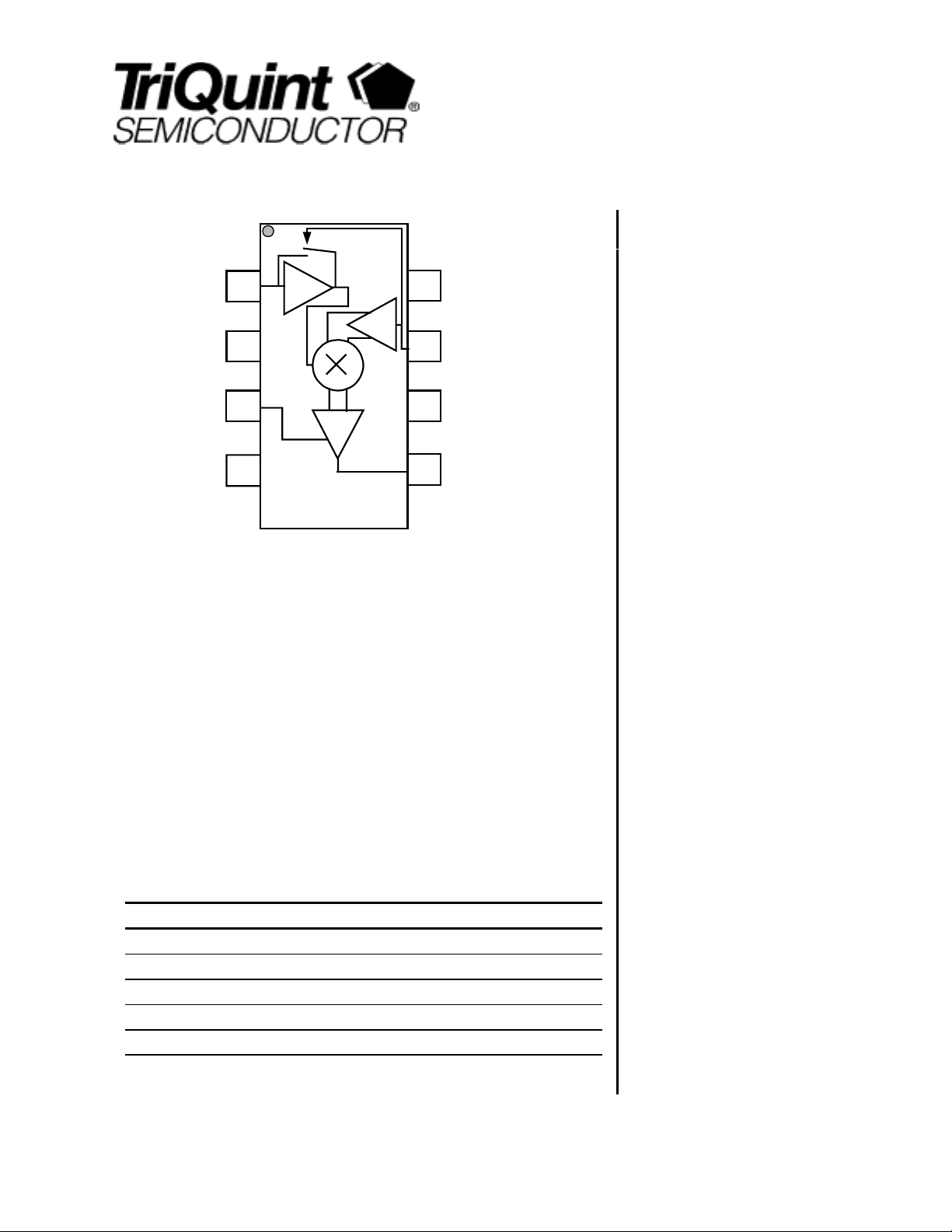
RF
INPUT
IF Common
Mode Tune
Mixer
Vdd
RF
IN
GND
Tune
VDD
VDD
LO
IN
GND
IF
out
RF Amplifier
Vdd
LO Input
RF amplifier
Control
IF
OUTPUT
Product Description
The TQ5633 is a 3V, RF Amplifier/Mixer IC designed specifically for PCS band
CDMA applications. It’s RF performance meets the requirements of products
designed to the IS-95 standard. The TQ5633 is designed to be used with an IF
frequency of 110MHz, and uses a balanced mixer to achieve ½ IF rejection. When
used with the TQ3631 or TQ3632 (CDMA LNAs) it provides a complete CDMA
receiver for 1900MHz phones.
The RF Amplifier/Mixer incorporates on-chip switches which determine two gain
select states. The RF and LO input ports are internally matched to 50
simplifying the design and keeping the number of external components to a
minimum. The TQ5633 achieves good RF performance with low current
consumption, supporting long standby times in portable applications. Coupled with
the very small SOT23-8 package, the part is ideally suited for PCS band mobile
phones.
Electrical Specifications
Parameter Min Typ Max Units
Frequency 1960 MHz
Gain 16.0 dB
Noise Figure 5.8 dB
Input 3rd Order Intercept -0.5 dBm
DC supply Current 23.0 mA
Note 1: Test Conditions: Vdd=2.8V , RF=1960MHz , LO=2070MHz, IF=110MHz, Ta=25C,
1
LO input –4dBm, CDMA High Gain state.
Ω
, greatly
DATA SHEET
3V PCS Band CDMA
RFA/Mixer IC
Features
Small size: SOT23-8
Single 3V operation
Low-current operation
Gain Select
High IP3 performance
Few external components
Excellent ½ IF rejection
110MHz IF Frequency
50 Ω RF and LO inputs
Applications
IS-95 CDMA Mobile Phones
Wireless Local Loop
PCS Micro-cell
For additional information and latest specifications, see our website: www.triquint.com 1
Page 2

TQ5633
Data Sheet
Electrical Characteristics
Parameter Conditions Min. Typ/Nom Max. Units
RF Frequency PCS band 1930 1960 1990 MHz
IF Frequency 100 110 130 MHz
LO Frequency 2030 2070 2120 MHz
CDMA Mode-High Gain
Gain 14.8 16.0 dB
Noise Figure 5.8 6.7 dB
Input IP3 -1.5 -0.5 dBm
½ IF IIP2 27 dBm
Supply Current 23.0 26.5 mA
CDMA Mode-Low Gain
Gain 5.8 7.0 dB
Noise Figure 10.0 dB
Input IP3 9.5 dBm
½ IF IIP2 32 dBm
Supply Current 18.5 mA
Supply Voltage 2.7 2.8 2.9 V
Note 1: Test Conditions: Vdd=2.8V , RF=1960MHz , LO=2070MHz, IF=110MHz, TC = 25° C, LO input –4dBm, unless otherwise specified.
°
Note 2: Min/Max limits are at +25
C case temperature, unless otherwise specified.
Absolute Maximum Ratings
Parameter Value Units
DC Power Supply 3.6 V
Power Dissipation 500 mW
Operating Temperature -30 to 85 C
Storage Temperature -60 to 150 C
Signal level on inputs/outputs +20 dBm
Voltage to any non supply pin -0.5 to +0.5 V
2 For additional information and latest specifications, see our website: www.triquint.com
Page 3
TQ5633
Data Sheet
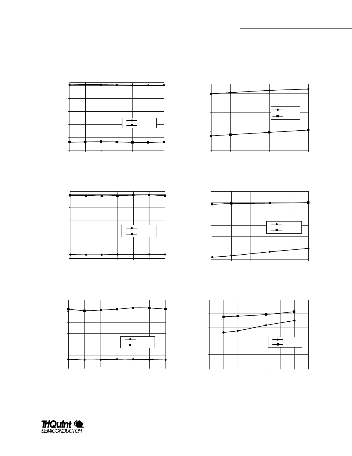
Typical Performance, Note:HG Mode=High Gain Mode, LG Mode=Low Gain Mode
Test Conditions, unless otherwise spec ified: Vdd=2.8V, Ta=25C, RF=1960MHz, LO=2070MHz , IF=110MHz, LO input=-4dBm
Conversion Gain vs Frequency
16
14
12
Gain (dB)
10
8
6
1930 1940 1950 1960 1970 1980 1990
Frequency (MHz)
Input IP3 vs. Frequency
9.5
7.5
5.5
IIP3 (dBm)
3.5
1.5
HG Mode
LG Mode
HG Mode
LG Mode
Conversion Gain vs. Vdd
18
16
14
12
10
Gain (dB)
8
6
4
2.7 2.8 2.9 3 3.1 3.2
Vdd (V)
Input IP3 vs. Vdd
11.5
9.5
7.5
5.5
IIP3 (dBm)
3.5
1.5
HG Mode
LG Mode
HG Mode
LG Mode
-0.5
1930 1940 1950 1960 1970 1980 1990
Frequency (MHz)
Noise Figure vs Frequency
11
10
9
8
7
Noise Figure (dB)
6
5
1930 1940 1950 1960 1970 1980 1990
Frequency (MHz)
HG Mode
LG Mode
-0.5
2.7 2.8 2.9 3 3.1 3.2
Vdd (V)
Half-IF Input IP2 vs. Vdd
40
35
30
25
IIP2 (dBm)
20
15
2.6 2.7 2.8 2.9 3 3.1 3.2 3.3
Vdd (V)
HG Mode
LG Mode
For additional information and latest specifications, see our website: www.triquint.com 3
Page 4
TQ5633
Data Sheet
Noise Figure vs. Vdd
11
10
9
8
7
Noise Figure (dB)
6
5
2.7 2.8 2.9 3 3.1 3.2
Vdd (V)
Idd vs. Vdd
30
28
26
24
22
Idd (mA)
20
18
16
2.7 2.8 2.9 3 3.1 3.2
Vdd (V)
HG Mode
LG Mode
HG Mode
LG Mode
Input IP3 vs. LO Power
11
9
7
5
IIP3 (dBm)
3
1
-1
-7 -6 -5 -4 -3 -2 -1
LO Power (dBm)
Half-IF Input IP2 vs. LO Power
40
35
30
25
IIP2 (dBm)
20
15
-7 -6 -5 -4 -3 -2 -1
LO Power (dBm)
HG Mode
LG Mode
HG Mode
LG Mode
Conversion Gain vs. LO Power
11
15
13
11
Gain (dB)
9
7
5
-7 -6 -5 -4 -3 -2 -1
LO Power (dBm)
HG Mode
LG Mode
10
9
8
7
Noise Figure (dB)
6
5
-7 -6 -5 -4 -3 -2 -1
4 For additional information and latest specifications, see our website: www.triquint.com
Noise Figure vs. LO Power
HG Mode
LG Mode
LO Power (dBm)
Page 5

TQ5633
Data Sheet
Idd vs. LO Power
24
23
22
21
20
Idd (mA)
19
HG Mode
LG Mode
18
17
16
-7 -6 -5 -4 -3 -2 -1
LO Power (dBm)
Conversion Gain vs. Temperature
18
16
14
12
10
8
Gain (dB)
6
HG Mode
LG Mode
4
2
0
-30 0 30 60 90
Temperature (C)
Half-IF Input IP2 vs. Temperature
40
35
30
25
IIP2 (dBm)
HG Mode
LG Mode
20
15
-30 -10 10 30 50 70 90
Temperature (C)
Noise Figure vs. Temperature
12
11
10
9
8
HG Mode
LG Mode
7
Noise Figure (dB)
6
5
4
-30 -10 10 30 50 70 90
Temperature (C)
Input IP3 vs. Temperature
11.5
9.5
7.5
5.5
IIP3 (dBm)
3.5
1.5
-0.5
-30 -10 10 30 50 70 90
Temperature (C)
For additional information and latest specifications, see our website: www.triquint.com 5
HG Mode
LG Mode
Idd vs. Temperature
28
26
24
22
20
18
Idd (mA)
16
14
HG Mode
LG Mode
12
10
-30 -10 10 30 50 70 90
Temperature (C)
Page 6
TQ5633
Data Sheet
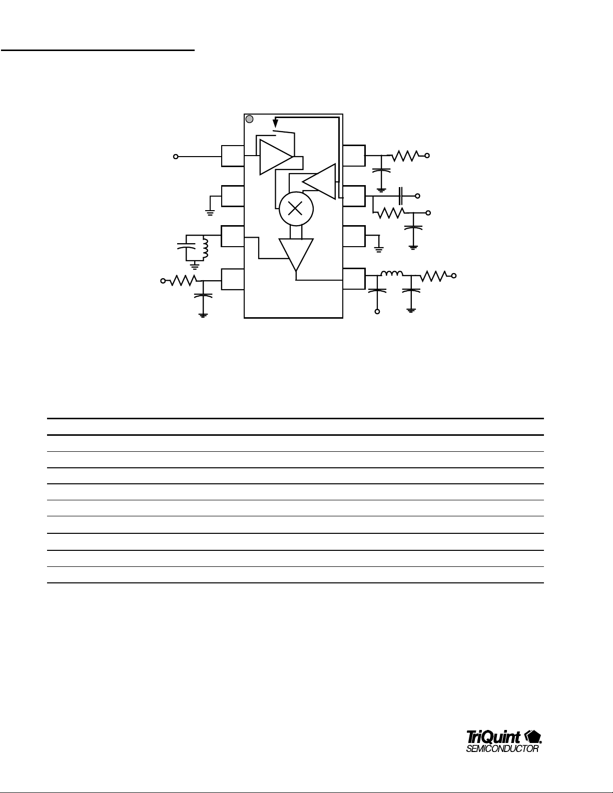
Application/Test Circuit
RF
INPUT
IF Common
Mode Tune
Mixer
Vdd
C3
R4
L2
C4
RF
IN
GND
Tune
VDD
VDD
LO
IN
GND
IF
out
C5
R1
L3 R5
C9
IF
OUTPUT
R3
C6
C7
RF Amplifier
Vdd
LO Input
Control 2
Gain Select
Vdd
IFA
C8
Bill of Material for TQ5633 RF AMP/Mixer
Component Reference Designator Part Number Value Size Manufacturer
Receiver IC U1 TQ5633 SOT23-8 TriQuint Semiconductor
Capacitor C3 3.3pF 0603
Capacitor C4, C6, C8 1000pF 0603
Capacitor C5, C7 5.6pF 0603
Capacitor C9 10pF 0603
Resistor R1
Resistor R3, R4, R5
Inductor L2 470nH 0805 Toko
Inductor L3 220nH 0805 Toko
2.2KΩ
3.3Ω
0603
0603
6 For additional information and latest specifications, see our website: www.triquint.com
Page 7

TQ5633
Data Sheet
TQ5631 Product Description
The TQ5633 is a balanced mixer down converter which
integrates the gain step functions required for PCS CDMA
handsets. The device requires minimal components and mates
with the TQ3631 or TQ3632 series of high band LNAs. The
TQ5633 was designed specifically for the needs of systems
using a low IF in the range of 85MHz to 130MHz, as it provides
a very high IP2. Some other outstanding features are 50ohm
matches at the RF input and LO input in both modes.
Simplified theory of operation
The TQ5633 contains a RF amplifier, balanced mixer, LO buffer,
IF amplifier and gain step switches. Figure 1 shows a block
diagram. In the high gain mode, the RF Amp is turned on and
the bypass switch is turned off. RF signal enters pin 1 and is
amplified by 10dB before arriving at the passive balanced mixer.
Total conversion gain is approximately 16dB.
The LO input at pin 8 is amplified by a saturating balanced
driver before being applied to the mixer. By using amplification
the LO drive remains constant over some range of LO input
power and temperature. The LO tuning is internal and centered
around 2070MHz.
The mixer utilizes proprietary techniques for attaining a very
high degree of balance. It converts the PCS band signal down
to approximately 110MHz using a high side LO source. By
utilizing a passive mixer it provides for excellent IP3 response.
The IF signal is taken off of the mixer and applied to an IF
amplifier which provides gain. The source of the IF stage is
brought out to pin 3 so an external tuned circuit can be used to
optimize IP2. The tuned circuit works by providing a high IF
impedance at the source of the output differential pair. High IF
common-mode rejection and balance are achieved by using a
high IF impedance.
RF
Input
Vdd
Mixer
R4
F1
C3 L2
C4
1
2
3
4
TQ5633
8
C5
7
6
5
C9
R3
C6
R1
C7
L3 R5
C8
Figure 1 TQ5633 Simplified Block Diagram and Schematic
Logic truth table and logic control functions
The TQ5633 logic control was designed to mate with the
TQ3631 or TQ3632 PCS Band LNAs. Although the TQ5633
has only one logic control line “C2”, it’s possible to obtain 4
different gain states when used in conjunction with the LNAs.
Moreover, only two logic lines are needed. On the TQ5633 the
“C2” control signal is superimposed on the LO input pin 7. A
simple 2.2k ohm resistor and blocking capacitor serve as the
decoupling network. Table 1 shows the logic control and device
states for a TQ3631-TQ5633 combination.
Control
Lines
C2 C3
0 0 High Gain High Gain High Gain
0 1 High Gain,
1 0 Mid Gain High Gain Low Gain
System
Mode
Low Linearity
LNA State TQ5633
State
High Gain,
High Gain
Low Linearity
Vdd
RFA
LO
Input
C2,
Gain
Select
Vdd
IFA
IF
Output
The low gain mode differs in that the RF amplifier is turned off
and passive switches route the RF input signal directly to the
mixer. In that case the total conversion gain is approximately
7dB.
For additional information and latest specifications, see our website: www.triquint.com 7
1 1 Low Gain Bypass Low Gain
Logic Table 1
Page 8

TUNING:
TQ5633
Data Sheet
IF Amplifier- The IF amplifier output at pin 5 requires a
match down to 50 ohms in addition to a source of DC bias. A
simple matching network that performs well for both functions is
a shunt-L series-C type. See Figure 1. The L3 inductor
provides DC bias to the IF amplifier while functioning as part of
the IF matching network. The C9 capacitor provides a DC block
and functions as the second AC matching component. During
the design phase it is usually fairly easy to empirically determine
these components by attaching a network analyzer to the
50ohm side of the IF network, and vary L3 and C9 until good
return loss at the IF frequency is obtained. Typical values for
L3 will be 180nH to 270nH and typical values of C9 are from
4.7pF to 15pF. Note that unlike a single-ended mixer type
design, a shunt-C element at the output is not required. The
TQ5633 leaks only a small amount of LO energy out of the RF
port, so no additional shunt-C filtering is required.
IF Tank Circuit- As discussed in the introduction, the
parallel LC circuit on pin 3 functions by creating a high IF
impedance at the sources of the IF amplifier, improving common
mode rejection. Once a prototype phone board layout is
finished there remains the task of assigning the values of these
components.
For a parallel circuit Rp = Q x Xp. Thus the higher Q and Xp
(i.e. Lp) are, the better IP2 will be. However, too high of a value
for L2 will make the circuit more prone to parasitic capacitances.
A good compromise would be to follow the evaluation board
example and start with a 3.3pF capacitor for C3. Then using a
network analyzer probe measure the impedance at the pin 3
pad with the TQ5633 absent. Adjust L2 until the network
analyzer measures S11 as close as possible to Γ = 1 at an
0
angle of 0
ohms is attainable with a 0805 size 470nH inductor. Smaller
package 0603 and 0402 inductors may not be obtainable in
such high values so that some compromises will have to be
made if inductor size is an issue. See Figure 2.
(i.e. an open circuit). In practice an |S11| of 7.5k
RF
Input
Vdd
Mixer
R4
F1
COAXIAL
PROBE
C3 L2
C4
S11
1
2
Ground at pad 2
3
4 5
REMOVE
TQ5633
FROM
BOARD
MEASURE S11
NETWORK
ANALYZER
8
C5
7
6
C9
R1
Marker at IF freq
e.g. 110MHz
Figure 2 IF Tank Tuning
Further Improving IP2:
Although the TQ5633 is exceptional in its isolation of the LO
signal from the RF port, there is still a miniscule amount of LO
energy present, typically –40dBc. That energy tends to bounce
off of the image filter and reenter the downconverter where,
depending on its phase, it creates a very small DC offset in the
mixer. The phenomena occurs in the Low Gain mode where it
can create 4 to 5 dBm variation in IP2 depending on how closely
the image filter is located to the TQ5633. Thus for applications
demanding the highest Half-IF spur rejection, higher IP2 can
possibly be obtained by tailoring the length of the transmission
line between the filter and chip. The specific line length will
depend upon board layout and will vary between filter types. If
it appears that the needed length will be long, the line can be
“U” shaped in order to conserve space. Measurements have
indicated that there is some reduction in gain at the optimum
line length.
R3
C6
C7
L3 R5
C8
Vdd
RFA
LO
Input
C2,
Gain
Select
Vdd
IFA
IF
Output
8 For additional information and latest specifications, see our website: www.triquint.com
Page 9
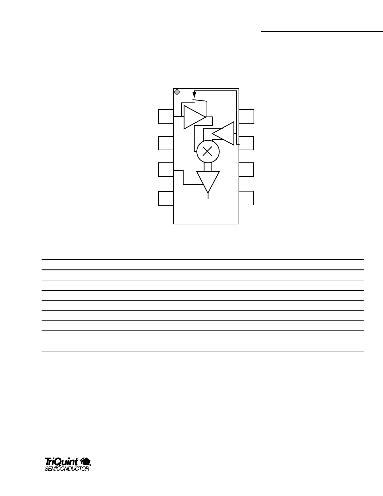
Package Pinout
TQ5633
Data Sheet
RF
INPUT
IF Common
Mode Tune
Mixer
Vdd
Pin Descriptions
Pin Name Pin # Description and Usage
RF INPUT 1 RF Amplifier Input
GND 2 Ground
Tune 3 IF Amplifier Common Mode Point
Vdd 4 Mixer Vdd
IF OUT 5 IF Output and IF Amplifier Vdd
GND 6 LO Common Mode Ground
LO INPUT 7 LO Input and RF Amplifier Gain Select
Vdd 8 RF Amplifier Vdd
RF
IN
GND
Tune
VDD
VDD
LO
IN
GND
IF
out
RF Amplifier
Vdd
LO Input
RF amplifier
Control
IF
OUTPUT
For additional information and latest specifications, see our website: www.triquint.com 9
Page 10

TQ5633
Data Sheet
Package Type: SOT23-8 Plastic Package
Note 1
PIN 1
FUSED LEAD
e
b
A
c
A1
E
E1
Note 2
DIE
L
θ
DESIGNATION DESCRIPTION METRIC ENGLISH NOTE
A OVERALL HEIGHT 1.20 +/-.25 mm 0.05 +/-.250 in 3
A1 STANDOFF .100 +/-.05 mm .004 +/-.002 in 3
b LEAD WIDTH .365 mm TYP .014 in 3
c LEAD THICKNESS .127 mm TYP .005 in 3
D PACKAGE LENGTH 2.90 +/-.10 mm .114 +/-.004 in 1,3
e LEAD PITCH .65 mm TYP .026 in 3
E LEAD TIP SPAN 2.80 +/-.20 mm .110 +/-.008 in 3
E1 PACKAGE WIDTH 1.60 +/-.10 mm .063 +/-.004 in 2,3
L FOOT LENGTH .45 +/-.10 mm .018 +/-.004 in 3
Theta FOOT ANGLE 1.5 +/-1.5 DEG 1.5 +/-1.5 DEG
Notes
1. The package length dimension includes allowance for mold mismatch and flashing.
2. The package width dimension includes allowance for mold mismatch and flashing.
3. Primary dimensions are in metric millimeters. The English equivalents are calculated and subject to rounding error.
Additional Information
For latest specifications, additional product information, worldwide sales and distribution locations, and information about TriQuint:
Web: www.triquint.com Tel: (503) 615-9000
Fax: (503) 615-8900
For technical questions and additional information on specific applications:
The information provided herein is believed to be reliable; TriQuint assumes no liability for inaccuracies or omissions. TriQuint assumes no responsibility for the use of
this information, and all such inform ation shall be entirely at t he user's own ri sk. Prices and specifications are subject to change without notice. No patent rights or
licenses to a ny of the circuits described herein are implied or granted to any third party.
TriQuint does not authorize or warrant any TriQuint product for use in life-support devices and/or systems.
Copyright © 2 000 TriQuint Semiconductor, Inc. All right s reserved.
Revision A, May, 2000
10 For additional information and latest specifications, see our website: www.triquint.com
 Loading...