

Page 1
WIRELESS COMMUNICATIONS DIVISION
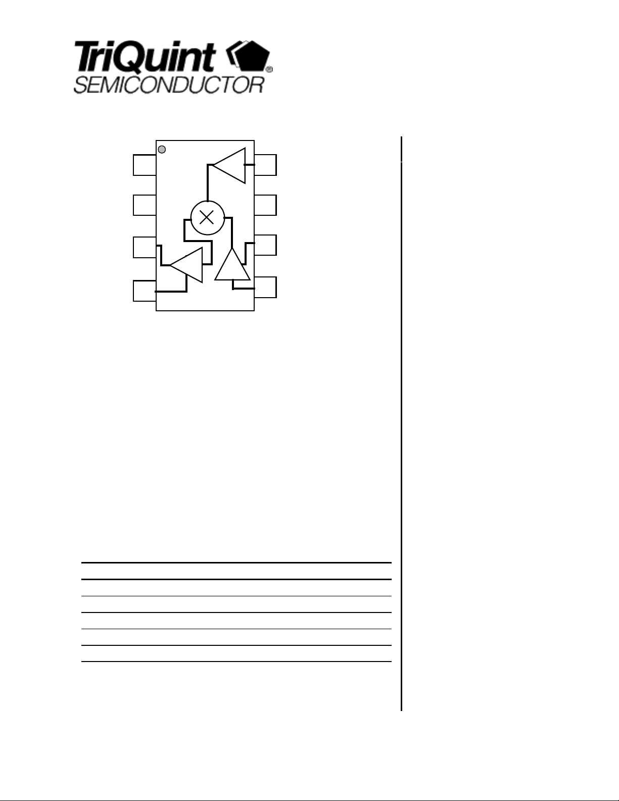
GND
GND
IF
out
GIC
RF
IN
VDD
VDD
LO
IN
Product Description
The TQ5631 is a 3V, RFAmplifier/Mixer IC designed specifically for PCS band CDMA
applications. It’s RF performance meets the requirements of products designed to
the IS-95 standards. The TQ5631 is designed to be used with the TQ3631 (CDMA
LNA) which provides a complete CDMA receiver for 1900MHz phones.
TQ5631
DATA SHEET
3V PCS Band CDMA
RFA/Mixer IC
Features
Small size: SOT23-8
Single 3V operation
Low-current operation
Gain Select
High IP3 performance
Few external components
The RFA/Mixer incorporates on-chip switches which determine gain select states.
When used with the TQ3631 (CDMA LNA), four gain steps are available. The RF
input port is internally matched to 50
the number of external components to a minimum. The TQ5631 achieves good RF
performance with low current consumption, supporting long standby times in portable
applications. Coupled with the very small SOT23-8 package, the part is ideally suited
for PCS band mobile phones.
Electrical Specifications
Parameter Min Typ Max Units
Frequency 1960 MHz
Gain 15.0 dB
Noise Figure 5.7 dB
Input 3rd Order Intercept 1.0 dBm
DC supply Current 20.0 mA
Note 1: Test Conditions: Vdd=2.8V , RF=1960MHz , LO=1750MHz, IF=210MHz, Ta=25C,
1
LO input –4dBm, CDMA High Gain state.
Ω
, greatly simplifying the design and keeping
Applications
IS-95 CDMA Mobile Phones
For additional information and latest specifications, see our website: www.triquint.com 1
Page 2

TQ5631
Data Sheet
Electrical Characteristics
Parameter Conditions Min. Typ/Nom Max. Units
RF Frequency PCS band 1800 1960 2200 MHz
IF Frequency 100 210 300 MHz
LO Frequency 1600 1750 2300 MHz
CDMA Mode-High Gain
Gain 12.2 15.0 dB
Noise Figure 5.7 6.8 dB
Input IP3 -1.0 1.0 dBm
Supply Current 20.0 25.5 mA
CDMA Mode-High Gain Low Linearity
Gain 17.0 21.0 dB
Noise Figure 5.3 dB
Input IP3 -3.0 dBm
Supply Current 20.0 mA
CDMA Mode-Mid Gain
Gain 1.0 3.0 dB
Noise Figure 12.0 dB
Input IP3 18.0 dBm
Supply Current 15.0 mA
CDMA Mode-Low Gain
Gain 6.2 8.0 dB
Noise Figure 10.0 dB
Input IP3 13.5 dBm
Supply Current 15.0 mA
Supply Voltage 2.7 2.8 2.9 V
Note 1: Test Conditions: Vdd=2.8V , RF=1960MHz , LO=1750MHz, IF=210MHz, TC = 25° C, LO input –4dBm, unless otherwise specified.
°
Note 2: Min/Max limits are at +25
C case temperature, unless otherwise specified.
Absolute Maximum Ratings
Parameter Value Units
DC Power Supply 5.0 V
Power Dissipation 500 mW
Operating Temperature -30 to 85 C
Storage Temperature -60 to 150 C
Signal level on inputs/outputs +20 dBm
Voltage to any non supply pin +0.3 V
2 For additional information and latest specifications, see our website: www.triquint.com
Page 3
TQ5631
Data Sheet
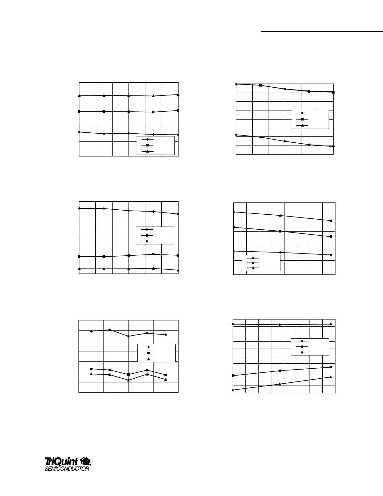
Typical Performance, Note:HG=High Gain, LL=High Gain Low Linearity, LG=Low Gain
Test Conditions, unless otherwise spec ified: Vdd=2.8V, Ta=25C, RF=1960MHz, LO=1750MHz , IF=210MHz, LO input=-4dBm ,
Conversion Gain vs. Freq.
25.00
20.00
15.00
10.00
Gain (dB)
5.00
0.00
LG Mode
HG Mode
LL Mode
1930 1940 1950 1960 1970 1980 1990
Freq. (MHz)
21.00
20.00
19.00
18.00
17.00
IDD (mA)
16.00
15.00
14.00
13.00
1930 1940 1950 1960 1970 1980 1990
IDD vs. Freq.
Freq. (MHz)
LG Mode
HG Mode
LL Mode
IIP3 vs. Freq.
16.00
11.00
6.00
IIP3 (dBm)
1.00
-4.00
1930 1940 1950 1960 1970 1980 1990
Freq. (MHz)
Noise Figure vs. Freq.
11.00
10.00
9.00
8.00
7.00
NF (dB)
6.00
5.00
4.00
1920 1940 1960 1980 2000
Freq. (MHz)
LG Mode
HG Mode
LL Mode
LG Mode
HG Mode
LL Mode
Conversion Gain vs. Temp.
25.00
20.00
15.00
10.00
Gain (dB)
5.00
LG Mode
HG Mode
LL Mode
0.00
-30-150 153045607590
Temp. (C)
IIP3 vs. Temp.
15.00
13.00
11.00
9.00
7.00
5.00
3.00
IIP3 (dBm)
LG Mode
HG Mode
LL Mode
1.00
-1.00
-3.00
-5.00
-30-150 153045607590
Temp. (C)
For additional information and latest specifications, see our website: www.triquint.com 3
Page 4
TQ5631
Data Sheet
Noise Figure vs. Temp.
12.00
11.00
10.00
9.00
8.00
7.00
NF (dB)
6.00
5.00
4.00
3.00
LG Mode
HG Mode
LL Mode
2.00
-30-150153045607590
Temp. (C)
IDD vs. Temp.
24.00
22.00
20.00
18.00
IDD (mA)
16.00
LG Mode
HG Mode
LL Mode
14.00
12.00
-30-150 153045607590
Temp. (C)
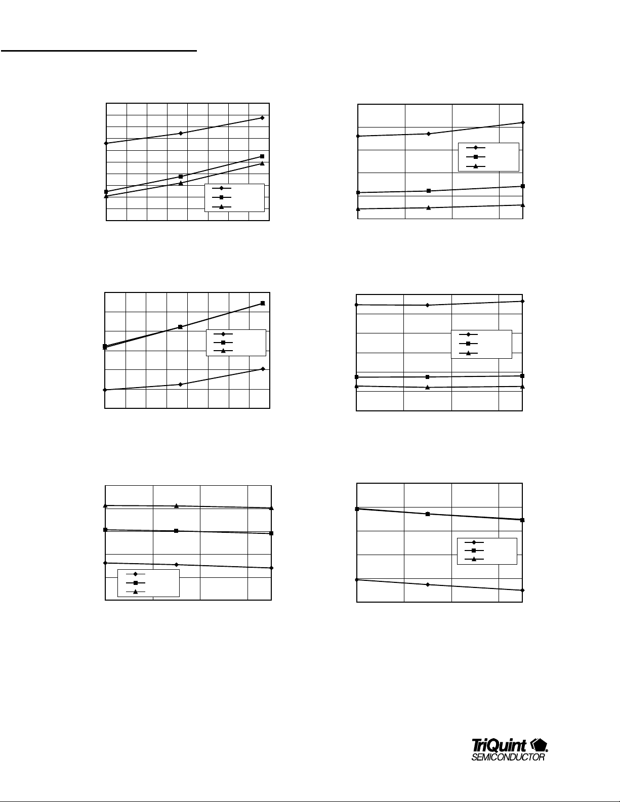
IIP3 vs. LO Power
20.00
15.00
10.00
5.00
IIP3 (dBm)
0.00
-5.00
-7 -5 -3 -1
LO Power (dBm)
Noise Figure vs. LO Power
10.00
9.00
8.00
7.00
NF (dB)
6.00
5.00
4.00
-7 -5 -3 -1
LO Power (dBm)
LG Mode
HG Mode
LL Mode
LG Mode
HG Mode
LL Mode
Conversion Gain vs. LO Power
25.00
20.00
15.00
Gain (dB)
10.00
5.00
LG Mode
HG Mode
LL Mode
0.00
-7 -5 -3 -1
LO Power (dBm)
23.00
21.00
19.00
17.00
IDD (mA)
15.00
13.00
-7 -5 -3 -1
4 For additional information and latest specifications, see our website: www.triquint.com
IDD vs. LO Power
LG Mode
HG Mode
LL Mode
LO Power (dBm)
Page 5

TQ5631
Data Sheet
Conversion Gain vs. VDD
23.00
21.00
19.00
17.00
15.00
Gain (dB)
13.00
11.00
9.00
7.00
2.7 2.8 2.9 3 3.1 3.2
VDD (V)
IIP3 vs. VDD
16.00
14.00
12.00
10.00
8.00
6.00
IIP3 (dB)
4.00
2.00
0.00
-2.00
-4.00
2.7 2.8 2.9 3 3.1 3.2
VDD (V)
LG Mode
HG Mode
LL Mode
LG Mode
HG Mode
LL Mode
IDD vs. VDD
24.00
22.00
20.00
18.00
IDD (mA)
16.00
14.00
12.00
2.7 2.8 2.9 3 3.1 3.2
VDD (V)
LG Mode
HG Mode
LL Mode
Noise Figure vs. VDD
10.00
9.00
8.00
7.00
NF (dB)
6.00
5.00
4.00
2.6 2.7 2.8 2.9 3 3.1 3.2 3.3
VDD (V)
For additional information and latest specifications, see our website: www.triquint.com 5
LG Mode
HG Mode
LL Mode
Page 6

TQ5631
Data Sheet
Application/Test Circuit
GND
RF
IN
Control 2
RF AMP
Gain
Select
L2
R9
RF input
C10
VDD
MXR
R10
VDD
MXR
C15
LO
IN
Out
C13
IF
C11
VDD
C12
L4
GND
IF
out
GIC
VDD
C19
VDD
L3
LO
IN
C20
R7
R8
C14
IF AMP
Gain
Select
Control 3
Bill of Material for TQ5631 RF AMP/Mixer
Component Reference Designator Part Number Value Size Manufacturer
Receiver IC U1 TQ5631 SOT23-8 TriQuint Semiconductor
Capacitor C11 22pF 0402
Capacitor C12, C14, C15, C19 1000pF 0402
Capacitor C13 12pF 0402
Capacitor C10 1.5pF 0402
Capacitor C20 68pF 0402
Resistor R8
Resistor R7, R9
Resistor R10
Inductor L2 2.7nH 0402 Panasonic
Inductor L3 4.7nH 0402 Panasonic
Inductor L4 56nH 0603 Panasonic
Filter U2 L2XB Fijitsu
27Ω
5.1KΩ
20Ω
0402
0402
0402
6 For additional information and latest specifications, see our website: www.triquint.com
Page 7

TQ5631
Data Sheet
TQ5631 Product Description
Simplified theory of operation
The TQ5631 contains an RF amp, mixer, IF amp, and RF
switches. Pin count is reduced by doubling the function of
several pins, where dc control bias and RF signal are present at
the same time. (Figure 1)
In the low gain modes, the RF amp is disabled and the the input
signal is routed directly to the mixer. In the high gain modes, a
cascode amp is switched in before the mixer. Control for this
function is made via a dc signal on the RF input pin 8. A
number of switches are used internally to eliminate any parasitic
signal paths.
The IF amp gain can be stepped as well via a control line at pin
5. The general IF amp gain and current draw can be set using
external components at the GIC pin 4.
The TQ5631 uses an off chip inductor with a bypass capacitor at
pin 6 for tuning the LO buffer. Although the device can be
connected directly to 50Ω at the RF input, a better match is
obtained by using a small series inductor and shunt capacitor at
the RF input .
RFA GAIN SELECT, C2
Logic truth table and logic control functions
TABLE 1 TRUTH TABLE
CONTROL LINES
Receiver RFA Gain IFA Gain LNA Mixer State
Mode Select Select State RFA IFA
C2 C3
CDMA HG 0 0 HG CDMA Idd HG LG
CDMA HGLL 0 1 HG Low Idd HG HG
CDMA MG 1 0 HG CDMA Idd Bypassed LG
CDMA LG 1 1 Bypassed Bypassed HG
HG=High Gain; HGLL=High Gain Low Linearity; MG=Mid Gain; LG=Low Gain
TABLE 1
When used in conjunction with the TQ3631, the TQ5631 down
convert mixer can be set to a variety of different gain states.
This allows the receiver (LNA + downconvert mixer) to operate
with a wide dynamic range, while optimizing current draw and
overall receiver performance.
Two external control lines set the LNA + downconverter into any
one of the four states, described below.
a) CDMA Low Gain Mode: This mode is selected in very high
signal environment. The current draw in this case is 16mA
for the receive chain.
b) CDMA High Gain Mode: This mode is selected in very
weak signal environment. The receiver is in it’s maximum
sensitivity.
IF OUT
RF IN
GND
1
GND
2
IF
3
GIC
4
VDD
GIC ADJUST
FIGURE 3
TQ5631 SIMPLIFIED CIRCUIT
c) CDMA High Gain Low Linearity Mode: This mode is
selected when the phone is in standby mode. The phone
power amplifier will be off in this state, removing the
possibility of self jamming.
8
7
6
5
RF
IN
VDD
LO TUNE
LO/C3
IF GAIN
SELECT, C3
VDD
d) CDMA Mid Gain Mode. This mode is selected in a medium
signal strength environment.
VDD
DOWNCONVERTER APPLICATION HINTS:
Printed Circuit Board Layout guidelines for
LO IN
For additional information and latest specifications, see our website: www.triquint.com 7
stability
With good layout practices the circuit will be stable. However,
poor layout may lead to oscillation problems. Good grounding is
especially important for the TQ5631 since it uses an off-chip LO
Page 8

TQ5631
Data Sheet
tuning inductor which provides a potential ground loop path.
One could use the evaluation board as an example of proper
layout techniques.
It is important to position the LO tuning and the GIC components
as close to the chip as possible. If the components are placed
too far from the chip the PC board traces can act as quarter
wave resonators in the 5-10GHz region. If both the GIC and the
LO paths to ground resonate at the same frequency, oscillation
can result, especially if Q is very high.
It is most important that the ground on the GIC bypass cap, the
LO tuning bypass capacitor, and the IF shunt cap return back to
chip pins 1 and 2 with minimal inductance. This requires that
ground returns utilize vias at a number of locations.
Solid grounding of the LO tuning inductor and bypass capacitor
will result in higher tuning circuit Q. The higher the Q, the
greater the LO drive to the mixer will be and IIP3 performance
will also improve with higher Q.
LO Buffer Tuning
from the die out to the pin which much be subtracted off of the
needed inductance value.
RF
IN
VDD
LO TUNE
LO/C3
LO IN
MEASURE S21
NETWORK
ANALYZER
COAXIAL
PROBE
SELECT, C3
VDD
IF GAIN
GND
GND
1
2
IF
3
GIC
4
PORT 1
8
7
6
5
Figure 2 LO Tuning Setup
Because of the broadband input match of the L0 buffer amplifier,
thermal and induced noise at other frequencies can be amplified
and injected directly into the L0 port of the mixer. Noise at the IF
frequency, and at L0 +/- IF will be downconverted and emerge
at the IF port, degrading the downconverter noise figure.
For maximum flexibility the high band TQ5631 device has the
output node of the L0 buffer amplifier brought out to Pin 6. By
connecting an external inductor between the pin and Vdd, LO
tuning can be varied. This inductor is selected to resonate with
internal capacitance at the L0 frequency in order to roll off outof-band gain and improve noise performance. This approach
allows selectivity in the L0 buffer amplifier along with the ability
to use the TQ5631 with multiple IF’s.
Calculation of Nominal L Value
The proper inductor value must be determined during the design
phase. The internal capacitance at Pin 6 is approximately 1.6
pF. Stray capacitance on the board surrounding Pin 6 will add to
the internal capacitance, so the nominal value of inductance can
be calculated, but must be confirmed with measurements on a
board approximating the final layout (see Figure 2).
Additionally, there is already approximately 1.3nH of inductance
The inductor is selected that would resonate with the total
capacitance at the L0 frequency using the following equation:
1
L = ---------------- - 1.3nH where C=1.6pF
C (2*pi*F)
2
To fine tune the LO, two methods have been proven to work
well:
a) Select the inductance (next standard value) which is higher
than the calculated value derived from the equation above.
Then select a bypass capacitor that forms a resonant
circuit with the inductor. The bypass capacitor can be used
to fine tune the resonant frequency.
b) The second method relies on moving the bypass capacitor
relative to the tuning inductor. This varies the amount of
inductance in the circuit and provides a means to fine tune
the LO. This method is utilized on the test boards.
8 For additional information and latest specifications, see our website: www.triquint.com
Page 9

TQ5631
Data Sheet
Verification of Proper LO Buffer Amp Tuning
Using a Network Analyzer
Connect port 1 to the L0 input (Pin 5) of the TQ5631 with the
source power set to deliver -4 dBm. Connect the coaxial probe
to Port 2 and place the probe tip approximately 0.1 inch away
from the inductor. The magnitude of S21 represents the L0
buffer frequency response (figure 3). The test can be done in
any of the CDMA modes, but both the rf and IF ports should be
terminated to 50 ohms.
Half IF Spur Rejection Considerations
Because the TQ5631 does not contain a balanced mixer, Half IF
spur rejection is completely set by the image filter. Thus we do
not recommend using an IF that is less than 2.5 times the
bandwidth of the image filter.
Downconverter IF Match Design
The Mixer IF output (pin 3) is an "open-drain" configuration,
allowing for flexibility in efficient matching to various filter types
and at various IF frequencies. An optimum lumped-element
matching network must be designed for maximum power gain
and output third order intercept.
When designing the IF output matching circuit, one has to
consider the output impedance (pin 3) of the IF Amplifier. It will
vary somewhat depending on the quiescent current, which is set
with the GIC pin. The IF frequency can be tuned from 100 to
300 MHz by varying component values of the IF output
matching circuit. The IF output pin also provides the DC bias for
the output FET’s.
Figure 3 LO Buffer Response
The absolute value isn't important, since it depends on the
probe's distance from the pin (it is usually around -30 dB), but
the peak of the response should be centered in the slightly to
the right of the L0 frequency band center, in this case 1750Mhz.
Increasing the inductance will lower the center frequency, and
vice versa. Try to keep the probe away from the LO input as it
will interfere with the measurement.
We have found experimentally that optimum mixer performance
is achieved when the LO is tuned slightly higher than the band
center. Additionally, since the curve is much steeper on the
high-side of the LO tuning curve, it is best to tune the device to a
slightly higher frequency to ensure that the application is never
operated in that region of the curve. Small variations in the
application circuit due to inductor tolerances and pc board trace
capacitance will then have less affect on the circuit.
Lower than expected IIP3 is the major symptom of improper LO
tuning in an application. The internal passive mixer FET needs
some minimum LO voltage at its gate in order to achieve
satisfactory IP3, which does not occur if the LO is untuned.
In the user's application, the IF output is most commonly
connected to a narrowband SAW or crystal filter with impedance
from 300 -1000Ω with 1 - 2 pF of capacitance. A conjugate
match to a higher filter impedance is generally less sensitive
than matching to 50Ω. When verifying or adjusting the matching
circuit on the prototype circuit board, the LO drive should be
injected at the nominal power level (-4 dBm), since the LO level
does have an impact on the IF port impedance.
Suggested Matching Networks
There are several networks that can be used to properly match
the IF port to the SAW or crystal IF filter. The IF FET current is
applied through the IF output pin 3, so the matching circuit
topology must contain either an RF choke or shunt inductor as
shown in Figure 4.
For purposes of evaluation, the shunt L, series C, shunt C circuit
shown below is the simplest and requires the fewest
components. DC current can be easily injected through the
shunt inductor and the series C provides a DC block, if needed.
The shunt C, in particular can be used to improve the return loss
and to reduce the LO leakage. Generally the shunt C should be
equal or larger than the series C. Furthermore, for best stability,
For additional information and latest specifications, see our website: www.triquint.com 9
Page 10

TQ5631
Data Sheet
the ground end of the shunt cap should be as close to the chip
ground as is possible.
Vdd
bypass
Chip
GIC PIN GIC PIN
GND
Chip
GND
L
IF
OUT
Cseries
Cshunt
50
ohms
Figure 4 IF Output Match
GIC Component Selection
The GIC pin on the TQ5631 is connected internally to the
source of the IF output stage. By adding two resistors and a
capacitor to this pin, it is possible to vary both the IF stage AC
gain, and the IF stage quiescent current. However, there is a
limit to the amount of gain increase that is possible, since there
always exists some package and bond wire inductance back to
the die. Furthermore, although some additional IP3
performance may be gained by increasing the quiescent current,
in practice it makes no sense to increase Idd beyond that which
provides maximum input intercept. At some point IP3 is limited
by the mixer FET, and no further increase in input intercept can
be obtained by adjusting the IF stage.
There are two GIC schemes that are recommended for the
CDMA devices (Figure 5). The first uses a small resistor in
series with a larger bypassed resistor. The AC gain is set by the
unbypassed resistor, while the DC IF current is then set by the
sum of the two resistors.
The second scheme, which is recommended for the high band
device, uses a resistor in parallel with a series combination of
resistor and capacitor. The first resistor sets the DC current,
while the equivalent parallel resistance sets the AC gain. The
presence of a resistor directly from the GIC pin to ground tends
to dampen the Q of any resonance in the 5-10ghz range which
might be formed by the GIC circuitry.
0 to 5 ohms
Zc bypass
at IF Freq
AC degen
20 to 60 ohms
sets IF
current
Minimize Board
Ground
Return Inductance
20 to 60 ohms
sets IF
current
0 to 5 ohms
AC degen
Zc bypass
at IF Freq
Minimize Board
Return Inductance
Figure 5 GIC Pin Networks
The Image Filter to Mixer RF input Path
We recommend evaluating the CDMA downconverter by
considering it and the image filter as a block, since there is a
very complicated non-linear interaction between the mixer and
image filter. Especially in the LG and MG receiver modes, some
LO energy leaks out through the RF input, reflects off the image
filter, and then returns back into the mixer (Figure 6).
The reflection at the filter occurs because most SAW and
dielectric filters look like a short circuit outside of the passband.
Depending on the phase of the reflected signal, noise figure,
gain, and IP3 can be negatively affected. Thus system
simulation can be inaccurate if the downconverter and filter are
treated separately.
LNA in Bypass
Mode
Mixer
IF
LO
band pass
LO Leakage
LO Leakage +
φ
Figure 6 Mixer-Filter Interaction
The issue also raises a dilemma with regard to the specification
of SSB noise figure. An image filter is needed for measurement;
yet how does one go about specifying the SSB noise figure (CG
Ground
10 For additional information and latest specifications, see our website: www.triquint.com
Page 11

and IIP3 as well) of the downconverter alone, realizing that it
depends somewhat upon the type of image filter used and the
delay between it and the mixer? The most pragmatic approach
measures the NF, CG, and IIP3 with the filter in place. The
downconverter to filter distance(in pS) is set to be similar to that
which would be used in the end application. Then filter I.L. is
simply subtracted off of the system noise figure in order to arrive
at the downconverter NF. Similarly, the filter I.L. is subtracted
off of the IIP3 and added to the CG in order to arrive at those
numbers.
Use correct RF input power levels for accurate
test results
Because the CDMA devices have a number of gain states, it
important to make sure that IP3 measurements are not taken in
a state of compression. Additionally, using too low of a power
puts the IMD products too close to the noise floor for accurate
results.
TQ5631
Data Sheet
Figure 7 shows the automated test setup that is used for
evaluation. Table 2 lists the RF input powers that we are using
to evaluate the devices, which has proved to be effective for
automated measurement. For bench measurement, it is
possible to use much lower input powers, since no hardware
routines are needed for peak searching.
RF Input Power (dBm)
Mode Downconverter
plus Filte r
CDMA HGLL -20
CDMA HG -20
CDMA MG -5
CDMA LG -10
Table 2 Suggested RF Input Test Levels
For additional information and latest specifications, see our website: www.triquint.com 11
Page 12

Package Pinout
TQ5631
Data Sheet
GND
GND
IF
out
GIC
Pin Descriptions
Pin Name Pin # Description and Usage
GND 1 Ground
GND 2 Ground
IF OUT 3 IF Output and IF Vdd
GIC 4 Off chip tuning for gain/IP3/current
LO IN 5 LO Input, and Control 3 input
VDD 6 LO Buffer Vdd
VDD 7 Mixer Vdd
RF IN 8 RF input, and Control 2 input
RF
IN
VDD
VDD
LO
IN
12 For additional information and latest specifications, see our website: www.triquint.com
Page 13

Package Type: SOT23-8 Plastic Package
Note 1
TQ5631
Data Sheet
PIN 1
FUSED LEAD
b
A
c
e
DESIGNATION DESCRIPTION METRIC ENGLISH NOTE
A OVERALL HEIGHT 1.20 +/-.25 mm 0.05 +/-.250 in 3
A1 STANDOFF .100 +/-.05 mm .004 +/-.002 in 3
b LEAD WIDTH .365 mm TYP .014 in 3
c LEAD THICKNESS .127 mm TYP .005 in 3
D PACKAGE LENGTH 2.90 +/-.10 mm .114 +/-.004 in 1,3
e LEAD PITCH .65 mm TYP .026 in 3
E LEAD TIP SPAN 2.80 +/-.20 mm .110 +/-.008 in 3
E1 PACKAGE WIDTH 1.60 +/-.10 mm .063 +/-.004 in 2,3
L FOOT LENGTH .45 +/-.10 mm .018 +/-.004 in 3
Theta FOOT ANGLE 1.5 +/-1.5 DEG 1.5 +/-1.5 DEG
Notes
1. The package length dimension includes allowance for mold mismatch and flashing.
2. The package width dimension includes allowance for mold mismatch and flashing.
3. Primary dimensions are in metric millimeters. The English equivalents are calculated and subject to rounding error.
A1
E
E1
Note 2
DIE
L
θ
For additional information and latest specifications, see our website: www.triquint.com 13
Page 14

TQ5631
Data Sheet
Additional Information
For latest specifications, additional product information, worldwide sales and distribution locations, and information about TriQuint:
Web: www.triquint.com Tel: (503) 615-9000
Fax: (503) 615-8900
For technical questions and additional information on specific applications:
The information provided herein is believed to be reliable; TriQuint assumes no liability for inaccuracies or omissions. TriQuint assumes no responsibility for the use of
this information, and all such inform ation shall be entirely at t he user's own ri sk. Prices and specifications are subject to change without notice. No patent rights or
licenses to a ny of the circuits described herein are implied or granted to any third party.
TriQuint does not authorize or warrant any TriQuint product for use in life-support devices and/or systems.
Copyright © 1 998 TriQuint Semiconductor, Inc. All right s reserved.
Revision A, March, 20 00
14 For additional information and latest specifications, see our website: www.triquint.com
 Loading...