

WIRELESS COMMUNICATIONS DIVISION
TQ5121
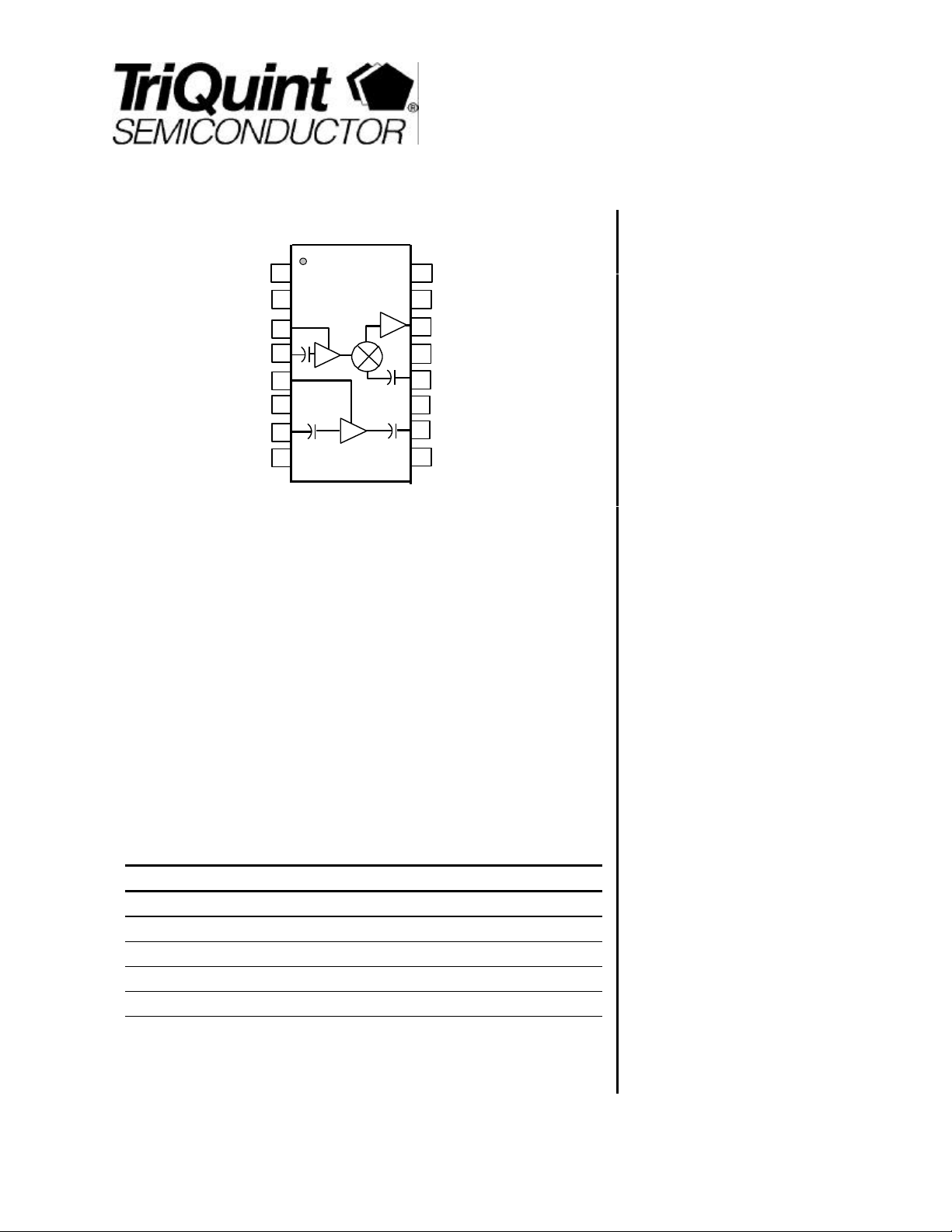
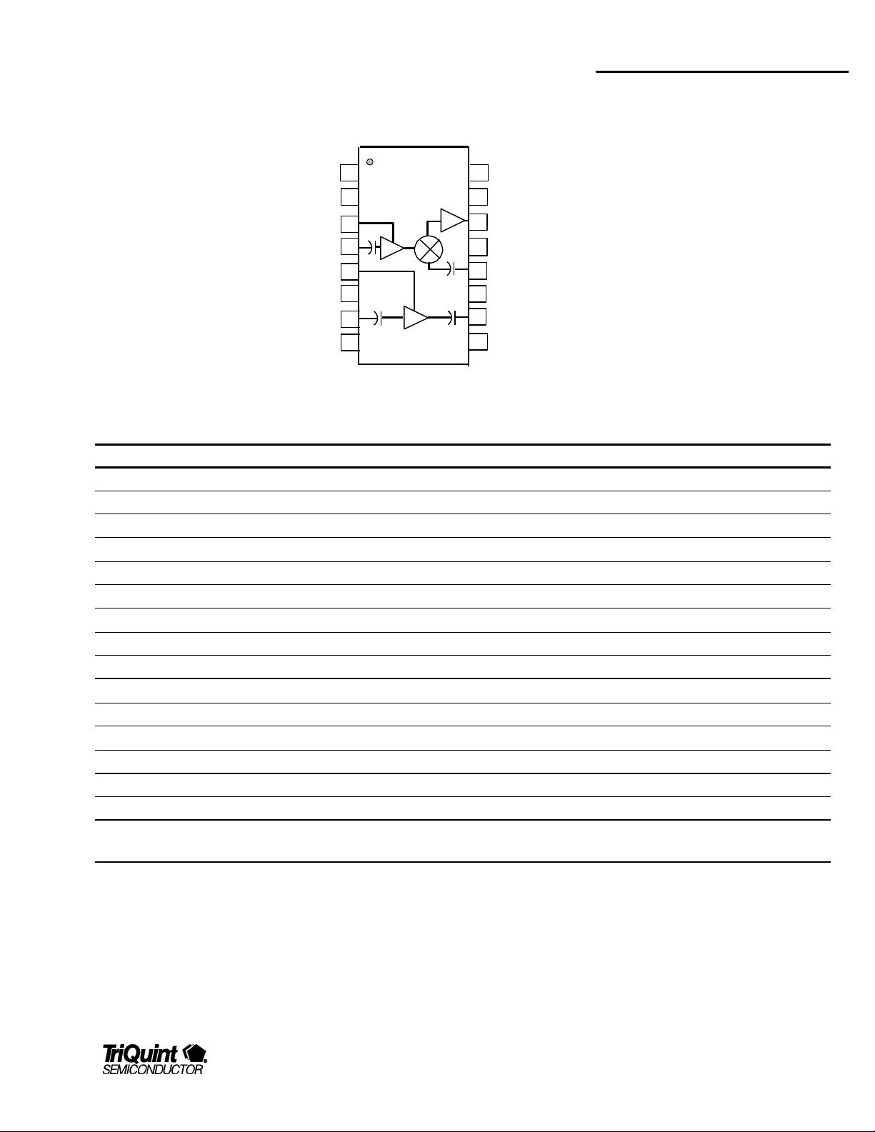
Optional
N/C
N/C
Vdd MXR
MXR LO
VDD LNA
GND
RF IN
GND
1
2
3
4
5
6
7
8
16
15
14
13
12
11
10
9
GND
N/C
Mixer IF/
Vdd
GND
MXR RF
GND
LNA
Out
N/C
Product Description
The TQ5121 is a 3V, RF receiver IC designed specifically for Cellular band TDMA
applications. It’s RF performance meets the requirements of products designed to
the IS-136 and AMPS standards. The TQ5121 is pin compatible with TQ9222, which
enables handset designers to use strategic board platform strategy. The TQ5121
contains LNA+Mixer circuits to handle the 800MHz cellular band.
DATA SHEET
3V Cellular TDMA/AMPS
LNA/mixer Receiver IC
Features
§ Pin compatible with TQ9222
(dual-band TDMA receiver)
§ Single 3V operation
§ Low-current operation
§ 50 Ω matched inputs
§ QSOP-16 plastic package
The mixer uses a high-side LO frequency, with the IF covering a range of 70 to
140MHz. Most RF ports are internally matched to 50 Ω, greatly simplifying the
design and keeping the number of external components to a minimum. The TQ5121
achieves good RF performance with low current consumption, supporting long
standby times in portable applications. Coupled with the very small QSOP-16
package, the part is ideally suited for Cellular band mobile phones.
Applications
§ IS-136 Mobile Phones
§ AMPS Mobile Phones
Electrical Specifications
Parameter Min Typ Max Units
Frequency 869 894 MHz
Gain 17.5 dB
Noise Figure 2.7 dB
Input 3rd Order Intercept -8.5 dBm
DC supply Current 10.0 mA
Note 1: Test Conditions: Vdd=2.8V, Ta=25C, filter IL=2.5dB, RF=881MHz, LO=991MHz, IF=110MHz,
LO input=-7dBm
For additional information and latest specifications, see our website: www.triquint.com 1
1
§ ISM 900MHz
TQ5121
Data Sheet
Electrical Characteristics
Parameter Conditions Min. Typ/Nom Max. Units
RF Frequency Cellular band 869 894 MHz
LO Frequency Cellular band 950 1040 MHz
IF Frequency Cellular band 70 140 MHz
LO input level -7 -4 0 dBm
Supply voltage 2.7 2.8 4.0 V
Gain 16.0 17.5 dB
Gain Variation vs. Temp. -40 to 85C -2.0 +2.0 dB
Noise Figure 2.7 3.5 dB
Input 3rd Order Intercept -11.0 -8.5 dBm
Return Loss LNA input – external match
LNA output
Mixer RF input
Mixer LO input
Isolation LO to LNA in
LO to IF; after IF match
RF to IF; after IF match
IF Output Impedance Vdd = 2.8V; “ON”
Vdd = 0V; “OFF”
Supply Current 10 13 mA
Temperature -40 25 85 C
Note 1: Test Conditions: Vdd=2.8V, filter IL=2.5dB, RF=881MHz, LO=991MHz, IF=110MHz, LO input=-7dBm, TC = 25° C, unless otherwise specified.
10
10
10
10
40
40
40
500
<50
dB
dB
dB
dB
dB
dB
dB
Ohm
Ohm
Absolute Maximum Ratings
Parameter Value Units
DC Power Supply 5.0 V
Power Dissipation 500 mW
Operating Temperature -55 to 100 C
Storage Temperature -60 to 150 C
Signal level on inputs/outputs +20 dBm
Voltage to any non supply pin +.3 V
2 For additional information and latest specifications, see our website: www.triquint.com
TQ5121
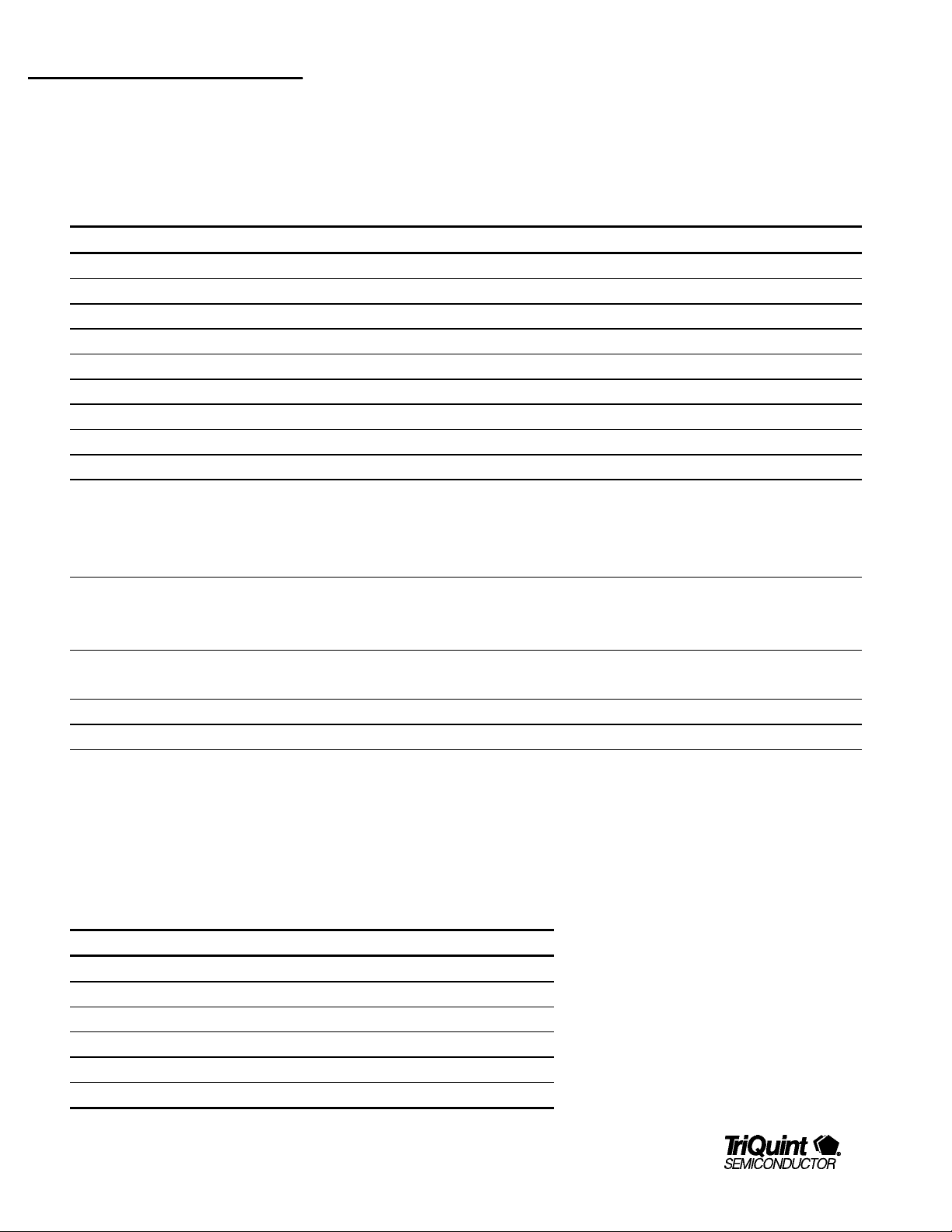
CG vs. Freq vs. Temp
CG vs. Temp vs. Vdd
CG vs. Vdd vs. Temp
Data Sheet
Typical Performance
Test Conditions (Unless Otherwise Specified): Vdd=2.8V, Ta=25C, filter IL=2.5dB, RF=881MHz, LO=991MHz, IF=110MHz, LO input=-7dBm
IIP3 vs. Vdd vs. Temp
20
19
18
17
16
15
Gain (dB)
14
13
12
11
10
869 872 875 878 881 884 887 890 893
20
19.5
19
18.5
18
17.5
Gain (dB)
17
16.5
16
15.5
15
-40 25 85
Freq (MHz)
Temp C
-40C
+25C
+85C
Vdd=2.7v
Vdd=2.8v
Vdd=3.0v
-6
-7
-8
-9
-10
IIP3 (dBm)
-11
-12
-13
-14
2.5 2.6 2.7 2.8 2.9 3 3.1 3.2
Vdd (volts)
IIP3 vs. Temp vs. Vdd
-7
-7.5
-8
-8.5
-9
IIP3 (dBm)
-9.5
-10
-10.5
-11
-40 25 85
Temp C
-40C
+25C
+85C
Vdd=2.7
Vdd=2.8
Vdd=3.0
20
18
16
Gain (dB)
14
12
10
2.5 2.6 2.7 2.8 2.9 3 3.1 3.2
Vdd (volts)
+25C
-40C
+85C
For additional information and latest specifications, see our website: www.triquint.com 3
Noise Figure vs. Freq vs. Temp
4
3.75
3.5
3.25
3
NF
2.75
2.5
2.25
2
869 872 875 878 881 884 887 890 893
Freq (MHz)
-40C
+25C
+85C

Data Sheet
Application/Test Circuit
TQ5121
16
15
14
13
12
11
10
N/C
C4
L3
Band
Pass
Filter
Lx
9
N/C
Mixer IF
C5
800
C6
Vdd
MXR
Vdd MXR
800
RF IN
800
C3
L2
MXR LO
800
VDD LNA
800
C1
L1
C2
N/C
N/C
1
2
3
4
5
6
7
8
Bill of Material for TQ5121 Receiver Application/Test Circuit
Component Reference Designator Part Number Value Size Manufacturer
Receiver IC U1 TQ5121 QSOP-16 TriQuint Semiconductor
Capacitor C1 1.2pF 0402
Capacitor C2, C3 1000pF 0402
Capacitor C4 10pF 0402
Capacitor C5
.01µF
Capacitor C6 8.2 pF 0402
Inductor L1, L2 10nH 0402
Inductor L3 180nH 0402
Inductor Lx (filter dependent) 10nH 0602
Toyocom (select) F1 T726881A 627-881A Toyocom
0402
4 For additional information and latest specifications, see our website: www.triquint.com

TQ5121
F
−
1
Vdd
Data Sheet
TQ5121 Product Description
The TQ5121 3V RFIC Downconverter is designed specifically
for cellular band TDMA applications. The TQ5121 contains a
LNA+Mixer circuit to handle the 800 MHz cellular band. The IF
frequency range covers 70 to 140 MHz with most of the ports
internally matched to 50 Ω simplifying the design and keeping
the number of external components to a minimum.
Operation
Please refer to the test circuit above.
Low Noise Amplifier (LNA)
The LNA section of the TQ5121 consists of a cascaded
common source FETs (see Fig 1). The LNA is designed to
operate on supply voltages from 3V to 5V. The source terminal
has to be grounded very close to the pin, this will avoid a
significant gain reduction due to degeneration. The LNA
requires a matching circuit on the input to provide superior
noise, gain and return loss performance. The output is close to
50 Ω for direct connection to a 50 Ω image stripping filter.
Fig 1. TQ5121
Simplified
Schematic of
LNA Section
LOAD
LNA
out
Fig 2. Suggested LNA Input Match
1.2pF
RF
IN
Note: These values assume ideal components and neglect board parasitic.
The discrepancy between these values and those of the typical application
circuit are the board and component parasitic
10nH
Pin 7
presented to the input pin. Highest gain and lowest return loss
occur when Γs is equal to the complex conjugate of the LNA
input impedance. A different source reflection coefficient, Γ
,
opt
which is experimentally determined, will provide the lowest
possible noise figure, F
min
.
The noise resistance, Rn, provides an indication of the sensitivity
of the noise performance to changes in Γs as seen by the LNA
input.
2
−
2 2
s
( )
F F
LNA MIN
= + ⋅
R
N opt S
4
Z
0
Γ Γ
opt
+ ⋅ −
1 1
Γ Γ
Components such as filters and mixers placed after the LNA
degrade the overall system noise figure according to the
following equation:
F F
SYSTEM LNA
= +
G
2
LNA
LNA
in
BIAS
BIAS
LNA Input Match
To obtain the best possible combination of performance and
flexibility, the LNA was designed to be used with off-chip
impedance matching on the input. Based on the system
requirements, the designer can make several performance
trade-offs and select the best impedance match for the
particular application.
The input matching network primarily determines the noise and
gain performance. Fig 2 shows a suggested input match using
a series 1.2pF capacitor and a shunt 10nH inductor.
The LNA gain, noise figure and input return loss are a function
of the source impedance (Zs), or reflection coefficient (Γs),
For additional information and latest specifications, see our website: www.triquint.com 5
F
LNA
and G
represent the linear noise factor and gain of the
LNA
LNA and F2 is the noise factor of the next stage. Thus, the
system noise figure depends on the highest gain and minimum
noise figure of the LNA.
Designing the input matching network involves a compromise
between optimum noise performance and best input return loss.
For example, when the TQ5121 LNA is matched for optimum
noise figure (1.35dB @ 880 MHz), the input return loss is
approximately 4dB. On the other hand, when the LNA is
matched for best return loss, the LNA noise figure is
approximately 1.95dB @ 881 MHz. See Table 1 for noise
parameters.

TQ5121
Data Sheet
Table 1. TQ5121 Noise Parameters
Freq |Gopt| <Gopt Fmin Rn
(MHz) (dB)
835 0.678 33 1.34 61.6
850 0.655 34 1.38 61.1
865 0.652 36 1.36 61.2
880 0.652 38 1.35 60.9
895 0.649 38 1.36 61.3
910 0.659 40 1.35 61.2
925 0.687 41 65.6
1.35
(W)
LNA Output Match
The output impedance of the LNA was designed to interface
directly with 50Ω terminations. This internal match serves to
reduce the number of external components required at this port.
An additional benefit accrues as an improvement in IP3
performance, return loss and power gain.
The output of the LNA will most often be connected to an image
stripping filter. Depending on the filter type, additional
components might be needed to present a better match to the
LNA output. The TQ5121 general applications circuit (page 4)
shows a TOYOCOM (637-881A) saw filter. A series inductor
“Lx” of 10nH is added to the filter input to improve the match.
This series inductor also smoothes out excessive ripple in the
filter passband improving the overall performance of the circuit.
Mixer
The mixer of the TQ5121 is implemented by a common source
depletion FET. The mixer is designed to operate on supply
voltages from 3V to 5V. An on-chip buffer amplifier simplifies
direct connection of the LO input to a commercial VCO at drive
levels down to -7dBm. The common-gate LO buffer provides a
good input match, and supplies the voltage gain necessary to
drive the mixer FET gate. The "open-drain " IF output allows for
Fig 3. Mixer Section
Mixer RF
Mixer IF
Output
Mixer LO
Input
LO Bias and
Tuning
Input
flexibility in matching to various IF frequencies and filter
impedance’s. See Figure 3.
Mixer: LO Port
As mentioned earlier, a common gate buffer amplifier is
positioned between the LO port and the mixer FET gate in order
to provide a good impedance to the VCO and to allow operation
at lower LO drive levels. The buffer amplifier provides the
voltage gain needed to drive the gate of the mixer FET while
consuming very little current (approximately 1.5mA).
Because of the broadband 50Ω input impedance of the buffer
amplifier and the internal DC blocking capacitor, the user’s VCO
can be directly connected to the LO input via a 50Ω line with no
additional components.
Mixer Input
Although the mixer input port has been designed with a
50Ω impedance, it has been found that LO leakage out through
the pin, can in some cases, reflect off the SAW filter and travel
back to the mixer input out of phase, causing some degradation
in conversion gain and system noise figure. Sensitivity to the
phenomena depends on the particular filter model and SAWmixer transmission line length.
LO Buffer Tune
While the broadband input match of the LO buffer amplifier
makes interfacing easy, the broadband gain means that thermal
and induced noise at other frequencies can be amplified and
injected directly into the LO port of the mixer. Noise at the IF
frequency, and at LO +/- IF will be downconverted and emerge
at the IF port, degrading the downconverter noise figure.
As indicated on the diagram of Fig 4, in order to test the LO
response to these spurious signals, a two-tone signal was
injected into the LO port with the RF port terminated in 50Ω.
One signal generator is set to the LO frequency at its normal LO
drive level usually (-7 dBm). The second signal generator
(spurious signal) is set to the LO +/- the IF frequency. The
combined input power at mixer LO port has to be less than -50
dBm. The results shown in Table 3 indicate a good suppression
of the interfering signals.
6 For additional information and latest specifications, see our website: www.triquint.com

Fig 4. LO Spurious Response Diagram
Fig 5.
LO Buffer Frequency
Fig 6
. Adjusting the
TQ5121
Mixer
RF IF
Spectrum
Analyzer
50 W
LO
Directional
+
Coupler
SIG 1:
flo
SIG 2:
flo +/- IF
Table 3. LO Spurious Response Data
LO/Spurious
(MHz)
Mixer LO Port
Input Power
C/V
(dB)
TQ5121
Data Sheet
Measuring the LO Frequency Response
The frequency response of the LO driver amplifier can be
measured using a semi-rigid probe (see Fig. 5) and a network
analyzer.
Connect port 1 to the LO input (Pin 4) of the TQ5121 with the
source power set to deliver -7 dBm. Connect the coaxial probe
to Port 2 and place the probe tip approximately 0.1 inch away
from either Pin 3 or the inductor.
Response
Network
Analyzer
Port 2
Port 1
3
Probe
4
TQ5121
991/1101 -57 -71.7
991/1101 -58.9 -71.8
Calculation of Nominal L Value
The node between the LO buffer amplifier and the mixer FET is
brought out to Pin 3 (L_tune) and connected to a shunt inductor
to AC ground. This inductor is selected to resonate with internal
capacitance at the LO frequency in order to suppress out-ofband gain and improve noise performance.
The internal capacitance of the LO amplifier output plus the
stray capacitance on the board surrounding Pin 3 is
approximately 1.8 pF. The inductor is selected to resonate with
the total capacitance at the LO frequency using the following
equation:
L
1
= ⋅ =
C f
2
Π
( )
where C pF
, .
2
15
Must be confirmed with measurements on a board
approximating the final layout.
-30
-32
-34
-36
-38
S21 (dB)
-40
-42
1000
1100 1200900800700
Frequency (MHz)
If the calculated shunt inductor (L2) is not a standard value, the
AC ground, implemented with C3, can be slide along the
transmission line to adjust for the right inductance (fig 6). Once
this is completed, the peak of the response should be centered
at the center of the LO frequency band.
AC Ground
Ground
3
TQ5121
Placement of inductor
will adjust between
standard values
For additional information and latest specifications, see our website: www.triquint.com 7

TQ5121
Data Sheet
Mixer IF Port
The Mixer IF output is an "open-drain" configuration, allowing for
flexibility in efficient matching to various filter types and at
various IF frequencies.
For evaluation of the LNA and mixer, it is usually necessary to
impedance match the IF port to the 50Ω test systems. When
verifying or adjusting the matching circuit on the prototype circuit
board, the LO drive should be injected at pin 4 at the nominal
power level of -7 dBm, since the LO level does have an impact
on the IF port impedance.
There are several networks that can be used to properly match
the IF port to the SAW or crystal IF filter. The mixer supply
voltage is applied through the IF port, so the matching circuit
topology must contain either an RF choke or shunt inductor. An
extra DC blocking capacitor is not necessary if the output will be
attached directly to a SAW or crystal bandpass filters.
Figure 7 shows the IF matching network, A shunt L, series C,
shunt C, is the simplest and requires the fewest components.
DC current can be easily injected through the shunt inductor and
the series C provides a DC block, if needed. The shunt C, is
used to reduce the LO leakage.
Fig 7. IF Output Match (110MHz)
180nH
10pF
0.01uF
8.2pF
10
Pin 14
Note: These values assume ideal components and neglect board parasitics.
The discrepancy between these values and those of the typical application
circuit are the board and component parasitics
Mx IF
out
Vdd
Ω
8 For additional information and latest specifications, see our website: www.triquint.com
TQ5121
Data Sheet
Package Pinout
Optional
1
N/C
2
N/C
Vdd MXR
MXR LO
VDD LNA
GND
RF IN
GND
3
4
5
6
7
8
Pin Descriptions
Pin Name Pin # Description and Usage
N/C 1 No Connection
N/C 2 No Connection
VDD_MXR 3 Mixer LO buffer supply voltage. Local bypass capacitor required.
MXR_LO 4
VDD_LNA 5 LNA supply voltage. Local bypass capacitor required.
GND 6 Ground
LNA_IN 7
GND_LNA 8 LNA first stage ground connection. Connection to ground.
N/C 9 No connection
LNA_OUT 10
GND 11 Ground
MXR_RF 12
GND 13 Ground
MXR_IF 14 Mixer IF output. Open drain output, connection to Vdd required. External matching is required.
N/C 15 No connection
Optional
16 Optional ground
GND
Mixer LO input. DC blocked, matched to 50Ω
LNA input. DC blocked. Requires external matching elements for noise match and match to 50Ω
LNA output. DC blocked. Matched to 50Ω.
Mixer RF input, DC blocked. Matched to 50Ω.
16
15
14
13
12
11
10
9
GND
N/C
Mixer IF/
Vdd
GND
MXR RF
GND
LNA
Out
N/C
For additional information and latest specifications, see our website: www.triquint.com 9
TQ5121
Data Sheet
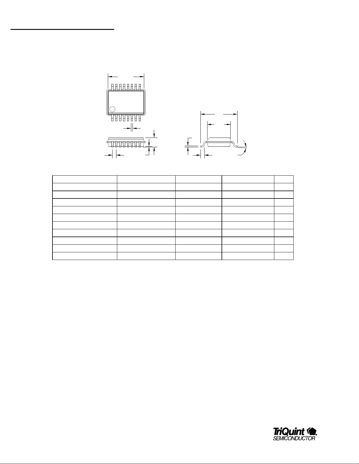
Package Type: Power QSOP-16 Plastic Package
D
NOTE A
b
A
E
E1
NOTE B
c
e
A1
L
θ
DESIGNATION DESCRIPTION ENGLISH METRIC NOTE
A OVERALL HEIGHT 0.064 +/-.005 in 1.63 +/-.13 mm C
A1 STANDOFF 0.007 +/-.003 in 0.18 +/-.08 mm C
b LEAD WIDTH 0.010 +/-.002 in 0.25 +/-.05 mm C
c LEAD THICKNESS 0.085 +/-.015 in 2.16 +/-.38 mm C
D PACKAGE LENGTH 0.193 +/-.004 in 4.90 +/-.10 mm A, C
e LEAD PITCH 0.025 BSC 0.635 BSC
E LEAD TIP SPAN 0.236 +/-.008 in 5.99 +/-.20 mm C
E1 PACKAGE WIDTH 0.154 +/-.003 in 3.91 +/-.08 mm B, C
L FOOT LENGTH 0.033 +/-.017 in 0.84 +/-.43 mm C
θ
FOOT ANGLE 4 +/-4 DEG 4 +/-4 DEG
NOTES:
A. THE D DIMENSION DOES NOT INCLUDE MOLD FLASHING AND MISMATCH. MOLD FLASHING AND MISMATCH SHALL NOT EXCEED .006 in (.15 mm)
PER SIDE.
B. THE E1 DIMENSION DOES NOT INCLUDE MOLD FLASHING AND MISMATCH. MOLD FLASHING AND MISMATCH SHALL NOT EXCEED .010 in (.25 mm)
PER SIDE.
C. PRIMARY UNITS ARE ENGLISH INCHES. THE METRIC EQUIVALENTS ARE SUBJECT TO ROUNDING ERROR.
Additional Information
For latest specifications, additional product information, worldwide sales and distribution locations, and information about TriQuint:
Web: www.triquint.com Tel: (503) 615-9000
Email: info_wireless@tqs.com Fax: (503) 615-8900
For technical questions and additional information on specific applications:
Email: info_wireless@tqs.com
The information provided herein is believed to be reliable; TriQuint assumes no liability for inaccuracies or omissions. TriQuint assumes no responsibility for the use of
this information, and all such information shall be entirely at the user's own risk. Prices and specifications are subject to change without notice. No patent rights or
licenses to any of the circuits described herein are implied or granted to any third party.
TriQuint does not authorize or warrant any TriQuint product for use in life-support devices and/or systems.
Copyright © 1998 TriQuint Semiconductor, Inc. All rights reserved.
Revision C, August 6, 1999
10 For additional information and latest specifications, see our website: www.triquint.com
 Loading...