

Page 1
WIRELESS COMMUNICATIONS DIVISION
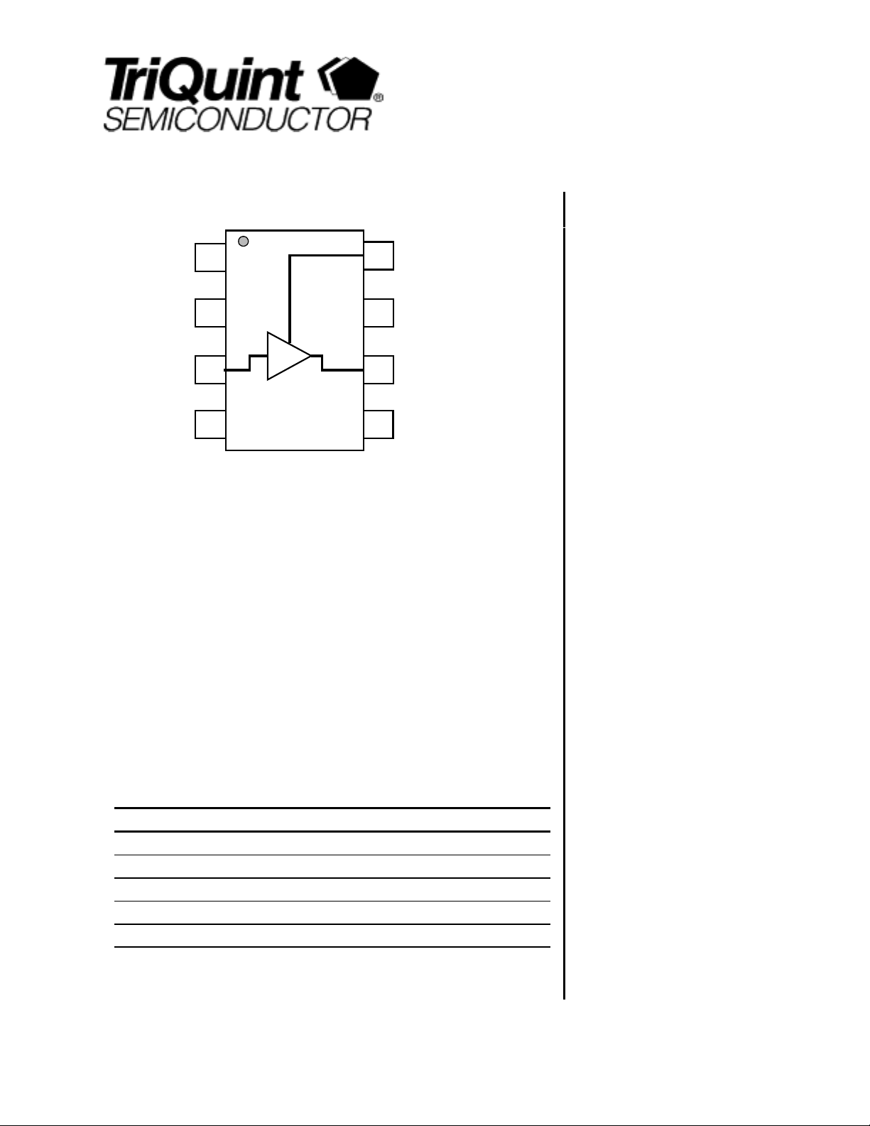
Control
Logic
C2
C2
L1
VDD
TQ3131
DATA SHEET
GND
RF
IN
GND
GND
RF
OUT
C3
50 ohm
RF Out
Control
Logic
Product Description
The TQ3131 is a 3V, RF LNA IC designed specifically for Cellular band CDMA/AMPS
applications. It’s RF performance meets the requirements of products designed to
the IS-95 and AMPS standards. The TQ3131 is designed to be used with the
TQ5131 (CDMA/AMPS mixer) which provides a complete CDMA receiver for
800MHz dual-mode phones.
The LNA incorporates on-chip switches which determine CDMA, AMPS, and bypass
mode select. When used with the TQ5131 (CDMA RFA/mixer), four gain states are
available. The RF output port is internally matched to 50
design and keeping the number of external components to a minimum. The TQ3131
achieves good RF performance with low current consumption, supporting long
standby times in portable applications. Coupled with the very small SOT23-8
package, the part is ideally suited for Cellular band mobile phones.
Electrical Specifications
Parameter Min Typ Max Units
Frequency 832 894 MHz
Gain 13.0 dB
Noise Figure 1.4 dB
Input 3rd Order Intercept 10.0 dBm
DC supply Current 10.5 mA
Note 1: Test Conditions: Vdd=2.8V , Tc=25C, RF fr equency=88 1MHz, CDMA High Gain state.
1
Ω
, greatly simplifying the
3V Cellular Band
CDMA/AMPS LNA IC
Features
Small size: SOT23-8
Single 3V operation
Low-current operation
Gain Select
Mode Select
High IP3 performance
Few external components
Applications
IS-95 CDMA Mobile Phones
AMPS Mobile Phones
Dual Mode CDMA Cellular applications
832-870MHz CDMA applications
For additional information and latest specifications, see our website: www.triquint.com 1
Page 2
TQ3131
Data Sheet
Electrical Characteristics
Parameter Conditions Min. Typ/Nom Max. Units
RF Frequency 832 881 894 MHz
CDMA Mode-High Gain
Gain 11.5 13.0 dB
Noise Figure 1.4 2.0 dB
Input IP3 8.0 10.0 dBm
LNA IN Return Loss (with external matching) 10 dB
LNA OUT Return Loss 10 dB
Supply Current 10.5 13.5 mA
Bypass Mode
Gain -3.0 -2.0 dB
Noise Figure 2.0 3.0 dB
Input IP3 18.0 30.0 dBm
LNA IN Return Loss (with external matching) 10 dB
LNA OUT Return Loss 10 dB
Supply Current 1.2 2.5 mA
AMPS Mode
Gain 8.5 11.0 dB
Noise Figure 1.6 2.2 dB
Input IP3 2.0 3.0 dBm
LNA IN Return Loss (with external matching) 10 dB
LNA OUT Return Loss 10 dB
Supply Current 4.0 5.5 mA
Supply Voltage 2.7 2.8 3.3 V
Note 1: Test Conditi ons: Vdd=2.8V, RF=881MHz, TC = 25° C, unless ot herwise specified.
Note 2: Min/Max limits are at +25
°
C case temperature, unless otherwise specified.
Absolute Maximum Ratings
Parameter Value Units
DC Power Supply 5.0 V
Power Dissipation 500 mW
Operating Temperature -40 to 85 C
Storage Temperature -60 to 150 C
Signal level on inputs/outputs +20 dBm
Voltage to any non supply pin +0.3 V
2 For additional information and latest specifications, see our website: www.triquint.com
Page 3
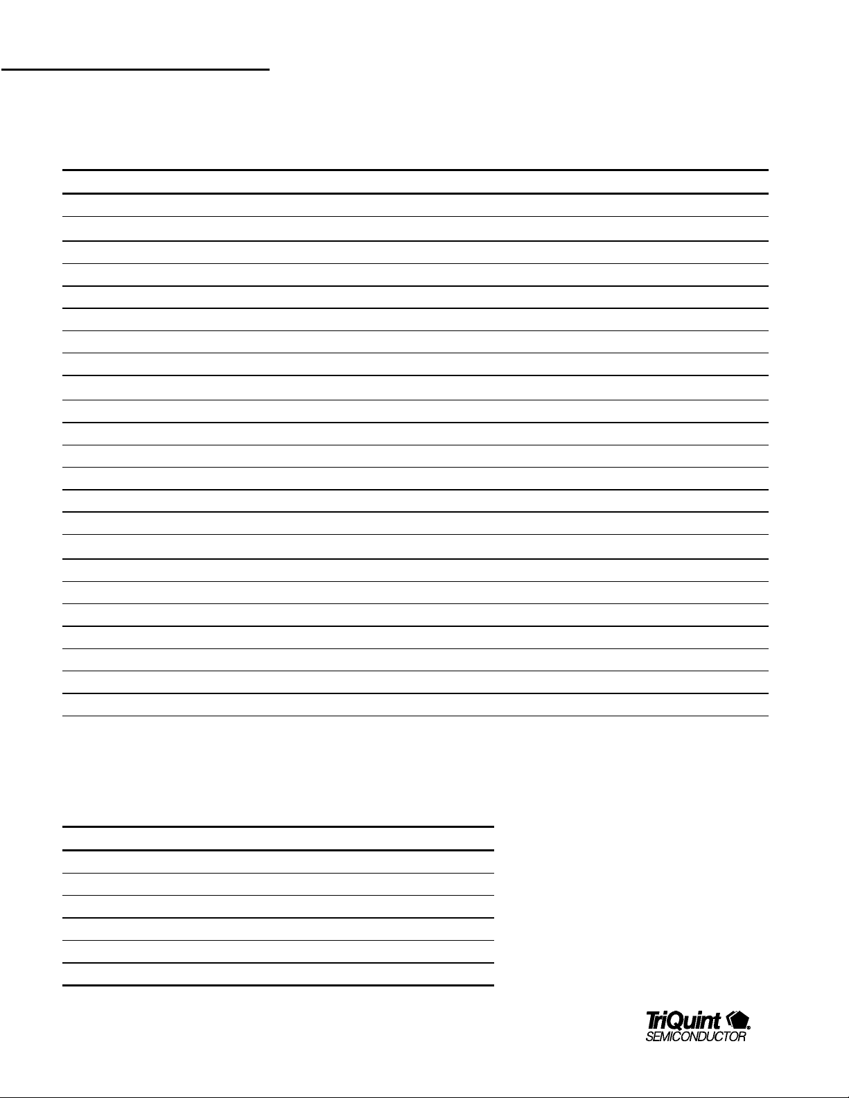
Typical Performance
Test Conditions, unless Otherwise Spec ified: Vdd=2.8V, Tc=+25C, RF=881MHz
CDMA High Gain Mode
Gain v Freq v Temp
15.0
14.5
14.0
13.5
13.0
12.5
12.0
Gain (dB)
11.5
11.0
10.5
10.0
850 860 870 880 890 900 910
Frequency (MHz)
-30C
+25C
+85C
TQ3131
Data Sheet
CDMA High Gain Mode
Idd v Vdd v Temp
13.50
13.00
12.50
12.00
11.50
11.00
Idd (mA)
10.50
10.00
9.50
9.00
2.5 2.7 2.9 3.1 3.3
Vdd (V)
-30C
+25C
+85C
CDMA High Gain Mode
IIP3 v Freq v Temp
13.5
13.0
12.5
12.0
IIP3 (dBm)
11.5
11.0
850 860 870 880 890 900 910
Frequency (MHz)
CDMA High Gain Mode
Noise Figure v Freq v Temp
1.90
1.70
1.50
1.30
1.10
Noise Figure (dB)
0.90
0.70
0.50
850 860 870 880 890 900 910
Frequency (MHz)
-30C
+25C
+85C
-30C
+25C
+85C
AMPS Mode
Gain v Freq v Temp
13.0
12.5
12.0
11.5
11.0
Gain (dB)
10.5
10.0
9.5
-30C
+25C
+85C
9.0
850 860 870 880 890 900 910
Frequency (MHz)
AMPS Mode
IIP3 v Freq v Temp
7.0
6.5
6.0
5.5
5.0
IIP3 (dBm)
4.5
4.0
3.5
3.0
850 860 870 880 890 900 910
Frequency (MHz)
-30C
+25C
+85C
For additional information and latest specifications, see our website: www.triquint.com 3
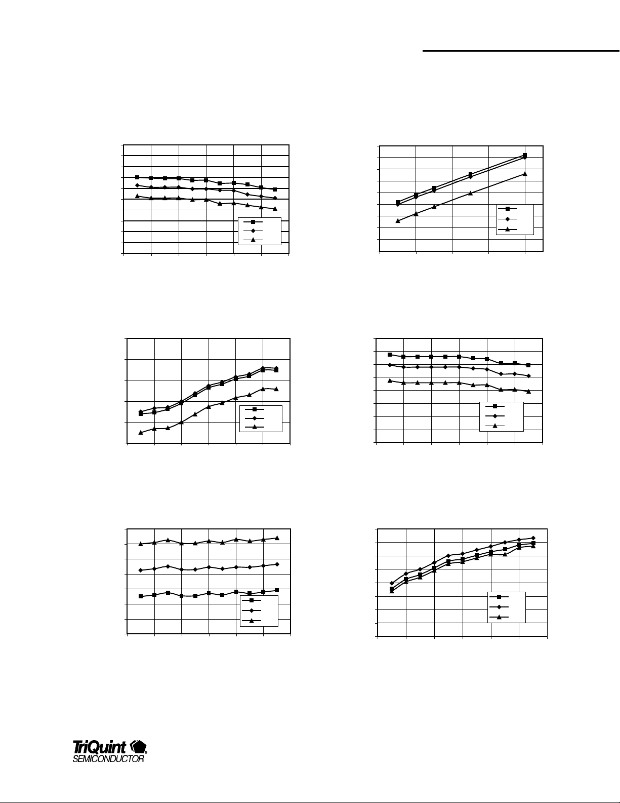
Page 4
TQ3131
Data Sheet
AMPS Mode
Noise Figure v Freq v Temp
2.50
2.00
1.50
1.00
Noise Figure (dB)
0.50
0.00
850 860 870 880 890 900 910
Frequency (MHz)
AMPS Mode
Idd v Vdd v Temp
5.50
5.00
4.50
Idd (mA)
4.00
3.50
3.00
2.5 2.7 2.9 3.1 3.3
Vdd (V)
-30C
+25C
+85C
-30C
+25C
+85C
BYPASS Mode
Gain v Freq v Temp
-1.0
-1.2
-1.4
-1.6
-1.8
-2.0
-2.2
Gain (dB)
-2.4
-2.6
-2.8
-3.0
850 860 870 880 890 900 910
Frequency (MHz)
BYPASS Mode
Noise Figure v Freq v Temp
2.50
2.00
1.50
1.00
Noise Figure (dB)
0.50
0.00
850 860 870 880 890 900 910
Frequency (MHz)
-30C
+25C
+85C
-30C
+25C
+85C
BYPASS Mode
IIP3 v Freq v Temp
35.0
34.0
33.0
32.0
31.0
30.0
IIP3 (dBm)
29.0
28.0
27.0
850 860 870 880 890 900 910
Frequency (MHz)
-30C
+25C
+85C
BYPASS Mode
Idd v Vdd v Temp
1.80
1.60
1.40
1.20
1.00
0.80
Idd (mA)
0.60
0.40
0.20
0.00
2.5 2.7 2.9 3.1 3.3
Vdd (V)
-30C
+25C
+85C
4 For additional information and latest specifications, see our website: www.triquint.com
Page 5
Application/Test Circuit
TQ3131
Data Sheet
Vdd
Control
Logic
C2
Vdd
C2
R1
GND
(paddle)
LNA input LNA output
L1
RF in
GND
RF
out
C1
Lbrd
LNA
GND
C3
Control Logic
Bill of Material for TQ3131 LNA Application/Test Circuit
Component Reference Designator Part Number Value Size Manufacturer
Receiver IC U1 TQ3131 SOT23-8 TriQuint Semiconductor
Capacitor C1 3.3pFd 0402
Capacitor C2 8.2pF 0402
Resistor R1
3.3Ω
Inductor L1 15nH 0402
Inductor Lbrd See application note
0402
For additional information and latest specifications, see our website: www.triquint.com 5
Page 6

TQ3131
Data Sheet
TQ3131 Product Description
The TQ3131 LNA uses a cascode low noise amplifier, along
with signal path switching. A bias control circuit sets the
quiescent current for each mode and ensures peak performance
over process and temperature, (refer to Figure 1). In the
application, CMOS level signals are applied to pins 1 and 5 and
are decoded by internal logic in order to set the device to the
desired mode. (see Table 1 for logic control states)
In the high gain mode, switches S1, S2, and S5 are closed, with
switches S3 and S4 open. In the bypass mode, switches S1,
S2, and S5 are open, with switches S3 and S4 closed. Having
five switches ensures that there are no parasitic feedback paths
for the signal. In the AMPS mode, control logic switches the
LNA into a low current bias condition.
Only three external components are needed in an application.
The chip uses an external cap and inductor for the input match
to pin 3. The output is internally matched to 50 ohms at pin 6.
A Vdd bypass cap is required close to pin 8.
Operation
MODE C2 C3 Typical Gain
High Gain 0
1
0
13(dB)
0
AMPS 0 1 11(dB)
Bypass 1 1 -2(dB)
Table 1 LNA States and Control Bits
LNA Input Network Design
Input network design for most LNA’s is a straightforward
compromise between noise figure and gain. The TQ3131 is no
exception, even though it has 3 different modes. The device
was designed so that one only needs to optimize the input
match in the high gain mode. As long as the proper grounding
and source inductance are used, the other two modes will
perform well with the same match.
External degeneration of the cascode is required between pin 4
and ground. However, a small amount of pc board trace can be
used as the inductor (Lbrd). Alternatively, if an extra component
can be tolerated, a small value chip inductor can be used. (see
Figure 2)
VDD
R1
VDD
8
C2
7
GND
LNA OUT
6
RF
OUT
5
C3
C3
LNA IN
C2
C1
L1
Lbrd
GND
RFIN
1
C2
Bias and Switch Control Logic
2
3
S1 S2
4
LNA
GND
S6
S3 S4
S5
Figure 1 TQ3131 Simplified Schematic
It is probably wise to synthesize the matching network
component values for some intermediate range of Gamma
values, and then by experimentation, find the one which
provides the best compromise between noise figure and gain.
The quality of the chip ground will have some effect on the
match, which is why some experimentation will likely be needed.
The input match will affect the output match to some degree, so
S22 should be monitored.
The values used on our evaluation board may be used as a
starting point.
Noise Parameter Analysis
A noise parameter analysis is shown on the next page for both
the high gain and AMPS modes. A “nominal” device was
mounted directly on a solid copper ground plane with semi-rigid
probes attached to the device input and output pins. A value of
Lbrd was chosen so that 13.0dB of gain was attained at
conjugate match. Then the tuner was removed and noise data
was taken. Please note that although data was taken at
700MHz and 1000MHz, the device was designed to operate
satisfactorily only over a much more limited range.
6 For additional information and latest specifications, see our website: www.triquint.com
Page 7

TQ3131
Data Sheet
Gamma Opt analysis for TQ3131 High Gain Mode
Freq
(MHz)
700 0.53 43.3 0.90 18.5
880 0.53 52.4 0.92 16.5
1000 0.48 58.5 1.01 15.4
Γ Opt Γ Angle
For additional information and latest specifications, see our website: www.triquint.com 7
Fmin (dB) R
noise
Page 8

TQ3131
Data Sheet
Gamma Opt analysis for TQ3131 Amps Mode
Freq (MHz)
700 0.61 40.6 1.22 33.0
880 0.70 54.2 1.09 27.4
1000 0.56 56.6 1.42 27.0
Γ Opt Γ Angle
Fmin (dB) R noise
Gain Control via Pin 4 Inductance
The source connection of the LNA cascode is brought out
separately through pin 4. That allows the designer to make
some range of gain adjustment. The total amount of inductance
present at the source of the cascode is equal to the bond wire
plus package plus external inductance. One should generally
use an external inductance such that gain in the high gain
CDMA mode = 13.0. Although it is possible to increase the gain
of the TQ3131 by using little or no degeneration, input intercept
will be degraded.
Figure 2 shows how a spiral pc board trace can be used as the
external inductance. It is suggested that such a circuit be used
for the initial design prototype. Then the optimum inductance
can be found by simply solder bridging across the inductor. The
final pc board design can then include the proper shorted
version of the inductor.
Figure 2 Showing Lbrd and Grounding on
Evaluation Board
8 For additional information and latest specifications, see our website: www.triquint.com
Page 9

Selection of the Vdd Bypass Cap for Optimum
TQ3131
Data Sheet
Performance
The Vdd bypass capacitor has the largest effect on the LNA
output match, and is required for proper operation. Because the
input match affects the output match to some degree as well,
the process of picking the bypass cap value involves some
iteration. First, an input match is selected which gives adequate
gain and noise figure. Then the bypass capacitor is varied to
give the best output match. Generally, the poorer the chip
grounding, the smaller the bypass capacitor value will be. The
demo board achieves 11-12dB of return loss which is adequate
for connection directly to the input of a SAW filter.
Grounding
An optimal ground for the device is important in order to achieve
datasheet specified performance.
TQ3131 High Gain Mode S-Parameters S11
Symptoms of a poor ground include reduced gain and the
inability to achieve >2:1 VSWR at the output when the input is
matched. It is recommended to use multiple vias to a mid
ground plane layer. The vias at pins 2 and 7 to this layer should
be as close to the lead pads as possible Additionally, the
ground return on the Vdd bypass cap should provide minimal
inductance back to chip pins 2 and 7.
TQ3131 S-Parameters
Following are S-Parameter graphs for both the high gain and the
AMPS modes. Data was taken on a single “nominal” device at
2.8v Vdd. The reference planes were set at the end of the
package pins. Note that the plots are almost identical for both
modes.
For additional information and latest specifications, see our website: www.triquint.com 9
Page 10

TQ3131
Data Sheet
S12
S21
10 For additional information and latest specifications, see our website: www.triquint.com
Page 11

TQ3131
Data Sheet
S22
TQ3131 Amps Mode S-Parameters S11
For additional information and latest specifications, see our website: www.triquint.com 11
Page 12

TQ3131
Data Sheet
S12
S21
12 For additional information and latest specifications, see our website: www.triquint.com
Page 13

TQ3131
Data Sheet
S22
For additional information and latest specifications, see our website: www.triquint.com 13
Page 14

TQ3131
Data Sheet
Control
Logic
C2
GND
RF
IN
GND
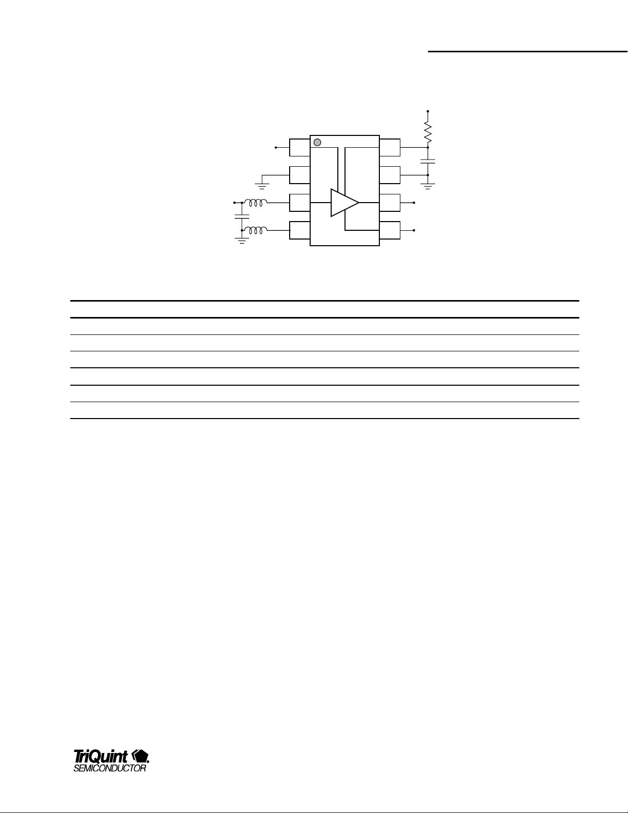
Package Pinout
Pin Descriptions
Pin Name Pin # Description and Usage
C2 1 Control logic 2
GND 2 Ground, paddle
RF IN 3 RF input, off-chip matching required
LNA GND 4 Ground
C3 5 Control logic 3
RF OUT 6 RF output, no matching required
LNA GND 7 Ground
Vdd 8 LNA Vdd, typical 2.8V, C2 capacitor required
C2
L1
VDD
GND
RF
OUT
C3
50 ohm
RF Out
Control
Logic
14 For additional information and latest specifications, see our website: www.triquint.com
Page 15

Package Type: SOT23-8 Plastic Package
Note 1
TQ3131
Data Sheet
PIN 1
FUSED LEAD
b
A
c
e
DESIGNATION DESCRIPTION METRIC ENGLISH NOTE
A OVERALL HEIGHT 1.20 +/-.25 mm 0.05 +/-.250 in 3
A1 STANDOFF .100 +/-.05 mm .004 +/-.002 in 3
b LEAD WIDTH .365 mm TYP .014 in 3
c LEAD THICKNESS .127 mm TYP .005 in 3
D PACKAGE LENGTH 2.90 +/-.10 mm .114 +/-.004 in 1,3
e LEAD PITCH .65 mm TYP .026 in 3
E LEAD TIP SPAN 2.80 +/-.20 mm .110 +/-.008 in 3
E1 PACKAGE WIDTH 1.60 +/-.10 mm .063 +/-.004 in 2,3
L FOOT LENGTH .45 +/-.10 mm .018 +/-.004 in 3
Theta FOOT ANGLE 1.5 +/-1.5 DEG 1.5 +/-1.5 DEG
A1
E
E1
Note 2
DIE
L
θ
Notes
1. The package length dimension includes allowance for mold mismatch and flashing.
2. The package width dimension includes allowance for mold mismatch and flashing.
3. Primary dimensions are in metric millimeters. The English equivalents are calculated and subject to rounding error.
For additional information and latest specifications, see our website: www.triquint.com 15
Page 16

TQ3131
Data Sheet
Additional Information
For latest specifications, additional product information, worldwide sales and distribution locations, and information about TriQuint:
Web: www.triquint.com Tel: (503) 615-9000
Email: info_wireless@tqs.com Fax: (503) 615-8900
For technical questions and additional information on specific applications:
Email: info_wireless@tqs.com
The information provided herein is believed to be reliable; TriQuint assumes no liability for inaccuracies or omissions. TriQuint assumes no responsibility for the use of
this information, and all such inform ation shall be entirely at t he user's own ri sk. Prices and specifications are subject to change without notice. No patent rights or
licenses to a ny of the circuits described herein are implied or granted to any third party.
TriQuint does not authorize or warrant any TriQuint product for use in life-support devices and/or systems.
Copyright © 1 998 TriQuint Semiconductor, Inc. All right s reserved.
Revision A, January, 2000
16 For additional information and latest specifications, see our website: www.triquint.com
 Loading...