

Page 1
1
TPV8200BMOTOROLA RF DEVICE DATA
The RF Line
The TPV8200B is designed for output stages in band IV and V TV transmitter
amplifiers. It incorporates high value emitter ballast resistors, gold metallizations and offers a high degree of reliability and ruggedness.
Including input and output matching networks, the TPV8200B features high
impedances. It can operate over the 470 MHz to 860 MHz bandwidth using a
single fixed tuned circuit.
• To be used class AB for TV band IV and V.
• Specified 28 Volts, 860 MHz Characteristics
Output Power = 190 Watts (peak sync.)
Output Power = 150 Watts (CW)
Gain = 8 dB Min
• Circuit board photomaster available upon request by contacting
RF Tactical Marketing in Phoenix, AZ.
MAXIMUM RATINGS
Rating Symbol Value Unit
Collector–Emitter Voltage V
CEO
30 Vdc
Collector–Base Voltage V
CBO
65 Vdc
Emitter–Base Voltage V
EBO
4 Vdc
Collector–Current — Continuous I
C
20 Adc
Total Device Dissipation @ TC = 25°C
Derate above 25°C
P
D
250
1.43
Watts
W/°C
Quiescent Current (without RF drive) I
CQ
2 x 500 mAdc
Storage Temperature Range T
stg
–65 to +150 °C
THERMAL CHARACTERISTICS
Characteristic Symbol Max Unit
Thermal Resistance, Junction to Case (1) R
θJC
0.7 °C/W
ELECTRICAL CHARACTERISTICS (T
C
= 25°C unless otherwise noted)
Characteristic
Symbol Min Typ Max Unit
OFF CHARACTERISTICS
Collector–Emitter Breakdown Voltage
(IC = 20 mAdc, IB = 0)
V
(BR)CEO
30 35 — Vdc
Collector–Base Breakdown Voltage
(IC = 20 mAdc, IE = 0)
V
(BR)CBO
65 80 — Vdc
Emitter–Base Breakdown Voltage (IE = 20 mAdc, IC = 0) V
(BR)EBO
4 5 — Vdc
Collector–Emitter Leakage Current (VCE = 28 Vdc, RBE = 75 Ω) I
CER
— — 15 mAdc
NOTE: (continued)
1. Thermal resistance is determined under specific RF condition.
Teflon is a registered trademark of du Pont de Nemours & Co., Inc.
Preferred devices are Motorola recommended choices for future use and best overall value.
Order this document
by TPV8200B/D
SEMICONDUCTOR TECHNICAL DATA
190 W, 470–860 MHz
RF POWER TRANSISTOR
NPN SILICON
CASE 375A–01, STYLE 1
Motorola Preferred Device
Motorola, Inc. 1994
REV 6
Page 2
TPV8200B
2
MOTOROLA RF DEVICE DATA
ELECTRICAL CHARACTERISTICS — continued (T
C
= 25°C unless otherwise noted)
Characteristic
Symbol Min Typ Max Unit
ON CHARACTERISTICS
DC Current Gain (ICE = 2 Adc, VCE = 10 Vdc) h
FE
30 75 120 —
DYNAMIC CHARACTERISTICS
Output Capacitance (each side) (2)
(VCB = 28 Vdc, IE = 0, f = 1 MHz)
C
ob
— 76 — pF
FUNCTIONAL TESTS IN CW
Common–Emitter Amplifier Power Gain
(VCE = 28 Vdc, P
out
= 150 W, ICQ = 2 x 75 mA, f = 860 MHz)
G
pe
8 9.5 — dB
Collector Efficiency
(VCE = 28 Vdc, P
out
= 150 W, ICQ = 2 x 75 mA, f = 860 MHz)
η 45 53 — %
Output Power @ 1 dB Compression (P
ref
= 40 W)
(VCE = 28 Vdc, ICQ = 2 x 75 mA, f = 860 MHz)
P
out
150 165 — W
Input overdrive: no degradation
(VCE = 28 Vdc, ICQ = 2 x 75 mA, f = 860 MHz)
P
in
30 — — W
Output Mismatch Stress:
(VCE = 28 Vdc, P
out
= 120 W, ICQ = 2 x 75 mA, f = 860 MHz,
Load VSWR = 3:1, all phase angles at frequency of test)
ψ
No Degradation in Output Power
Before or After Test
FUNCTIONAL TESTS IN VIDEO (Standard Black Level)
Peak Output Power @ 1 dB Compression
(VCE = 28 Vdc, ICQ = 2 x 75 mA, f = 860 MHz)
P
out
190 210 — W
NOTE:
2. Value of “Cob” is that of die only. It is not measurable in TPV8200B because of internal matching network.
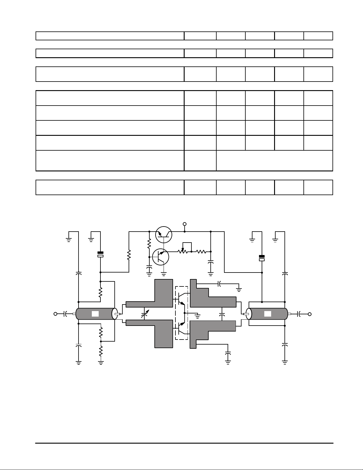
Figure 1. 860 MHz Test Circuit
INPUT OUTPUT
C1
C6
C6
C8
R2
R2
R1
R3
R4
C10
T1
T2
P1
R5
C11
C3
C4
C3
C9
C7
C5
C7
C2
V
CC
L1 L2
C1 — Chip Capacitor 47 pF ATC 100A
C2 — Chip Capacitor 12 pF ATC 100B
C2 — + Trimmer Capacitor 0.5–4 pF
C3 — Chip Capacitor 8.2 pF ATC 100B
C4 — Chip Capacitor 12 pF ATC 100B
C5 — Chip Capacitor 100 pF ATC 100A
C6 — Chip Capacitor 2 x 1000 pF Vitramon
C7 — Chip Capacitor 2 x 0.1 µF Vitramon
C8 — Capacitor 220 µF/16 V
C9 — Capacitor 100 µF/40 V
C10 — Chip Capacitor 100 pF Vitramon
C11 — Chip Capacitor 15 nF Vitramon
L1 — Coaxial 25 Ω/length = 41 mm
L2 — Coaxial 25 Ω/length = 41 mm
R1 — Chip Resistor 47 Ω
R2 — 2 x 1 Ω (0.5 Ω)
R3 — Resistor 0.8 Ω
R4 — Resistor 47 Ω
R5 — Resistor 1.2 kΩ
P1 — Trimmer Resistor 5 kΩ
T1 — Transistor BD 135
T2 — Transistor BD 135
PC Board: 1/50″ Glass Teflon ∈r = 2.55
D.U.T.
Page 3
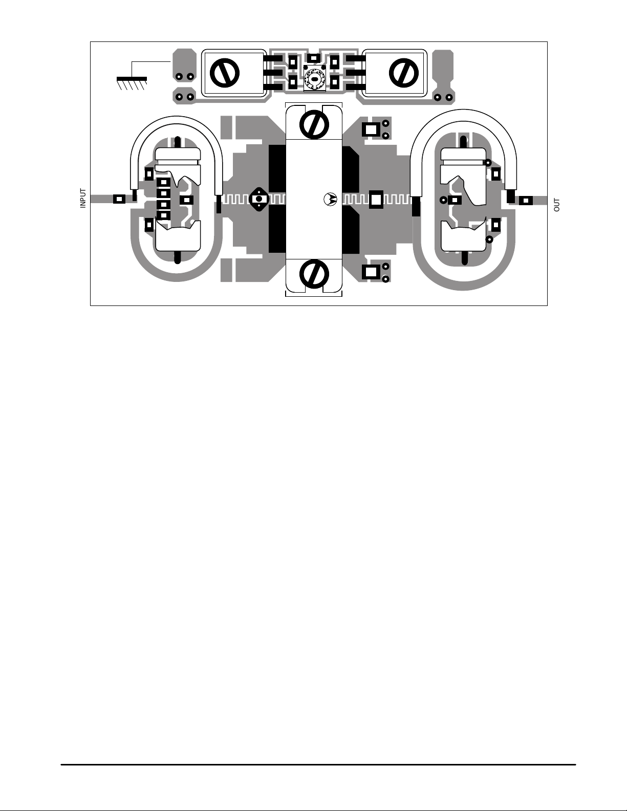
3
TPV8200BMOTOROLA RF DEVICE DATA
Figure 2. Components View
CAUTION
The TPV8200B is a high power transistor and thermal adaptation is very important for good RF performance
(see mechanical drawing for mounting recommendations).
Maximum Ratings are given to avoid destruction of the transistor; another limitation is MMMTBF and the
user must first determine the minimum wanted life–time in order to choose the right way of use for the device
(see MMMTBF curves), especially in case of CW application.
INPUT
OUTPUT
Page 4

TPV8200B
4
MOTOROLA RF DEVICE DATA
TYPICAL CHARACTERISTICS
230
210
190
170
150
130
470 665 860
VCE = 28 V
ICQ = 2 x 75
mA
f, FREQUENCY (MHz)
P
o
, OUTPUT POWER (WATTS)
13
12
11
10
9
8
470 665 860
VCE = 28 V
ICQ = 2 x 75 mA
P
out
= 150 W
f, FREQUENCY (MHz)
G
pe
, POWER GAIN (dB)
150
100
50
0
0 10 20
VCE = 28 V
ICQ = 2 x 75 mA
f = 860 MHz
P
o
, OUTPUT POWER (WATTS)
INPUT POWER (WATTS)
60
50
40
30
20
10
0
0 50 100 150
VCE = 28 V
ICQ = 2 x 75 mA
f = 860 MHz
OUTPUT POWER (WATTS)
, EFFICIENCY (%)
η
–20
–30
–40
–50
50 100 150 200 250
VCE = 28 V
ICQ = 2 x 75 mA
f = 860 MHz
INTERMODULATION (dB)
Po, OUTPUT POWER (WATTS)
IMD
–5 dB
–17 dB
–20
–30
–40
–50
25 50 75 100
INTERMODULATION (dB)
Po, OUTPUT POWER (WATTS)
VCE = 28 V
ICQ = 2 x 75 mA
f = 860 MHz
IMD
0 dB
–7 dB
Figure 3. Output Power @ 1 dB Comp.
versus Frequency
Figure 4. Power Gain versus Frequency
Figure 5. Output Power versus Input Power Figure 6. Collector Efficiency versus Output Power
Figure 7. Intermodulation versus Peak Power
(Side Band)
Figure 8. Intermodulation versus Peak Power
(Dual Sound)
Page 5

5
TPV8200BMOTOROLA RF DEVICE DATA
100
90
80
70
60
50
40
30
20
10
0
100
90
80
70
60
50
40
30
20
10
0
P
out
= 100 W P
out
= 150 W P
out
= 210 W P
out
= 210 W
APL 10–90 (%)
TEST CONDITIONS:
10% Rest Carrier
Channel 69
VCE = 28 V
ICQ = 2 x 75 mA
100
0
40
TYPICAL VIDEO CHARACTERISTICS @ f = 860 MHz
VCE = 28 V
% %
100
90
80
70
60
50
40
30
20
10
0
%
(Input Video Waveform) (Input Video Waveform)
27%
0%
(Input Video Waveform) (Input Video Waveform)
VCE = 28 V
ICQ = 2 x 75 mA
f = 860 MHz
(Channel 69)
Black Level
200
150
100
50
5 10 15 20 25
P
o
, OUTPUT POWER (WATTS)
Pin, INPUT POWER (WATTS)
30
25
20
15
0 50 100 150 200
SYNC. PULSE (%)
Po, OUTPUT POWER (WATTS)
VCE = 28 V
ICQ = 2 x 75 mA
f = 860 MHz
(Channel 69)
Black Level
Figure 9. Peak Output Power versus Peak
Input Power
Figure 10. Sync. Pulse versus Peak
Output Power
Figure 11. Gain versus Output Power
Page 6

Figure 12. Series Equivalent Input/Output Impedances
Base–base & collector–collector Impedances with
Circuit Tuned for Maximum Gain @ VCE = 28 V/ICQ = 2 x 75 mA/P
out
= 150 W
RELIABILITY DEPENDENCE ON THERMAL CONSIDERATIONS
MMMTBF: Metal Migration Mean Time Before Failure.
Figure 13. Thermal Resistance versus
Junction Temperature
Figure 14. MMMTBF versus Junction Temperature
TYPICAL CONDITIONS (120 W CW):
P
out
= 120 W
Pin = 15 W
VCE = 28 V
η = 45%
ICQ = 9.5 A
RTH = 0.7°C/W
T
max
= 70°C
P
diss
= 161 W
T
jct
= 183°C
J = (5.64) 104 A/cm
2
MTBF =
26 YEARS
P
out
= 70 W
Pin = 7.8 W
VCE = 28 V
η = 38%
ICQ = 6.6 A
RTH = 0.7°C/W
T
max
= 70°C
P
diss
= 123 W
T
jct
= 156°C
J = (3.92) 104 A/cm
2
MTBF =
252 YEARS
TYPICAL CONDITIONS (210 W VIDEO):
0.80
0.75
0.70
0.65
0.60
0.55
50 100 150 200 250
JUNCTION TEMPERATURE (
°
C)
R
th
, JUNCTION – CASE ( C/W)
°
10
11
10
10
10
9
10
8
10
7
10
6
50 100 150 200 250
JUNCTION TEMPERATURE (
°
C)
MMMTBF (HOURS. A
2
)
f = 860 MHz
Z
in
ZOL*
f = 470 MHz
860
470
Zo = 10
Ω
TPV8200B
6
MOTOROLA RF DEVICE DATA
f
MHz
Z
in
Ohms
Z
OL*
Ohms
470 0.80 + j2.11 7.93 + j0.94
567 0.85 + j3.15 5.94 + j0.30
665 1.56 + j4.20 4.55 – j0.02
762 2.64 + j3.36 3.70 – j0.52
860 2.72 + j2.24 2.91 – j0.92
Z
OL*
= Conjugate of optimum load impedance into which
ZOL* = the device operates at a given output power,
ZOL* = voltage, current, and frequency.
Page 7

7
TPV8200BMOTOROLA RF DEVICE DATA
PACKAGE DIMENSIONS
CASE 375A–01
ISSUE O
NOTES:
1. DIMENSIONING AND TOLERANCING PER ANSI
Y14.5M, 1982.
2. CONTROLLING DIMENSION: INCH.
STYLE 1:
PIN 1. COLLECTOR
2. COLLECTOR
3. BASE
4. BASE
5. EMITTER
1 2
3 4
5
D
Q
G
L
R
K
2 PL
–B–
–T–
M
B
M
0.25 (0.010) T
E
H
F
C
SEATING
PLANE
A
N
DIM MIN MAX MIN MAX
MILLIMETERSINCHES
A 1.330 1.350 33.79 34.29
B 0.375 0.395 9.52 10.03
C 0.180 0.205 4.57 5.21
D 0.320 0.340 8.13 8.64
E 0.060 0.070 1.52 1.77
F 0.004 0.006 0.11 0.15
G 1.100 BSC 27.94 BSC
H 0.082 0.097 2.08 2.46
K 0.580 0.620 14.73 15.75
L 0.435 BSC 11.05 BSC
N 0.845 0.875 21.46 22.23
Q 0.118 0.130 3.00 3.30
R 0.390 0.410 9.91 10.41
Page 8

TPV8200B
8
MOTOROLA RF DEVICE DATA
Motorola reserves the right to make changes without further notice to any products herein. Motorola makes no warranty , representation or guarantee regarding
the suitability of its products for any particular purpose, nor does Motorola assume any liability arising out of the application or use of any product or circuit,
and specifically disclaims any and all liability, including without limitation consequential or incidental damages. “T ypical” parameters can and do vary in different
applications. All operating parameters, including “T ypicals” must be validated for each customer application by customer’s technical experts. Motorola does
not convey any license under its patent rights nor the rights of others. Motorola products are not designed, intended, or authorized for use as components in
systems intended for surgical implant into the body, or other applications intended to support or sustain life, or for any other application in which the failure of
the Motorola product could create a situation where personal injury or death may occur. Should Buyer purchase or use Motorola products for any such
unintended or unauthorized application, Buyer shall indemnify and hold Motorola and its officers, employees, subsidiaries, affiliates, and distributors harmless
against all claims, costs, damages, and expenses, and reasonable attorney fees arising out of, directly or indirectly, any claim of personal injury or death
associated with such unintended or unauthorized use, even if such claim alleges that Motorola was negligent regarding the design or manufacture of the part.
Motorola and are registered trademarks of Motorola, Inc. Motorola, Inc. is an Equal Opportunity/Affirmative Action Employer.
Literature Distribution Centers:
USA: Motorola Literature Distribution; P.O. Box 20912; Phoenix, Arizona 85036.
EUROPE: Motorola Ltd.; European Literature Centre; 88 T anners Drive, Blakelands, Milton Keynes, MK14 5BP, England.
JAPAN: Nippon Motorola Ltd.; 4-32-1, Nishi-Gotanda, Shinagawa-ku, Tokyo 141, Japan.
ASIA PACIFIC: Motorola Semiconductors H.K. Ltd.; Silicon Harbour Center, No. 2 Dai King Street, Tai Po Industrial Estate, Tai Po, N.T., Hong Kong.
TPV8200B/D
*TPV8200B/D*
◊
 Loading...