

Page 1
1
TPV597MOTOROLA RF DEVICE DATA
The RF Line
. . . designed for 1.0 watt stages in Band V TV transposer amplifiers. Gold
metallized dice and diffused e mitter ballast resistors are used to enhance
reliability, ruggedness and linearity.
• Band IV and V (470–860 MHz)
• 1.0 W — P
ref
@ –58 dB IMD
• 20 V — V
CC
• High Gain — 11 dB Typ, Class A @ f = 860 MHz
• Gold Metallization for Reliability
MAXIMUM RATINGS
Rating Symbol Value Unit
Collector–Emitter Voltage V
CEO
24 Vdc
Collector–Base Voltage V
CBO
45 Vdc
Emitter–Base Voltage V
EBO
3.5 Vdc
Collector Current — Continuous I
C
1.4 Adc
Total Device Dissipation @ TC = 25°C
Derate above 25°C
P
D
19
0.11
Watts
W/°C
Operating Junction Temperature T
J
200 °C
Storage Temperature Range T
stg
–65 to +200 °C
THERMAL CHARACTERISTICS
Characteristic Symbol Max Unit
Thermal Resistance, Junction to Case R
θJC
9.0 °C/W
ELECTRICAL CHARACTERISTICS
Characteristic Symbol Min Typ Max Unit
OFF CHARACTERISTICS
Collector–Emitter Breakdown Voltage (IC = 40 mA, IB = 0) V
(BR)CEO
24 — — Vdc
Collector–Base Breakdown Voltage (IC = 2.0 mA, IE = 0) V
(BR)CBO
45 — — Vdc
Emitter–Base Breakdown Voltage (IE = 4.0 mA, IC = 0) V
(BR)EBO
3.5 — — Vdc
Emitter–Base Leakage Current (VEB = 2.0 V) I
EBO
— — 0.5 mA
Collector–Emitter Breakdown Voltage (IC = 40 mA, RBE = 10 Ω) V
(BR)CER
50 — — Vdc
Collector Cutoff Current (VCB = 30 V, IE = 0) I
CBO
— — 1.2 mAdc
ON CHARACTERISTICS
DC Current Gain (IC = 200 mA, VCE = 5.0 V) h
FE
15 — 120 —
DYNAMIC CHARACTERISTICS
Output Capacitance (VCB = 28 V, IE = 0, f = 1.0 MHz) C
ob
— — 7.0 pF
FUNCTIONAL TESTS
Common–Emitter Amplifier Power Gain
(VCE = 20 V, P
out
= 1.0 W, f = 860 MHz, IE = 0.44 A)
G
PE
10.5 11 — dB
Load Mismatch
(VCE = 20 V, P
out
= 2.0 W, IE = 0.44 A, f = 860 MHz,
Load VSWR = ∞:1, All Phase Angles)
ψ
No Degradation in Output Power
(continued)
Order this document
by TPV597/D
SEMICONDUCTOR TECHNICAL DATA
1.0 W, 470–860 MHz
UHF LINEAR
POWER TRANSISTOR
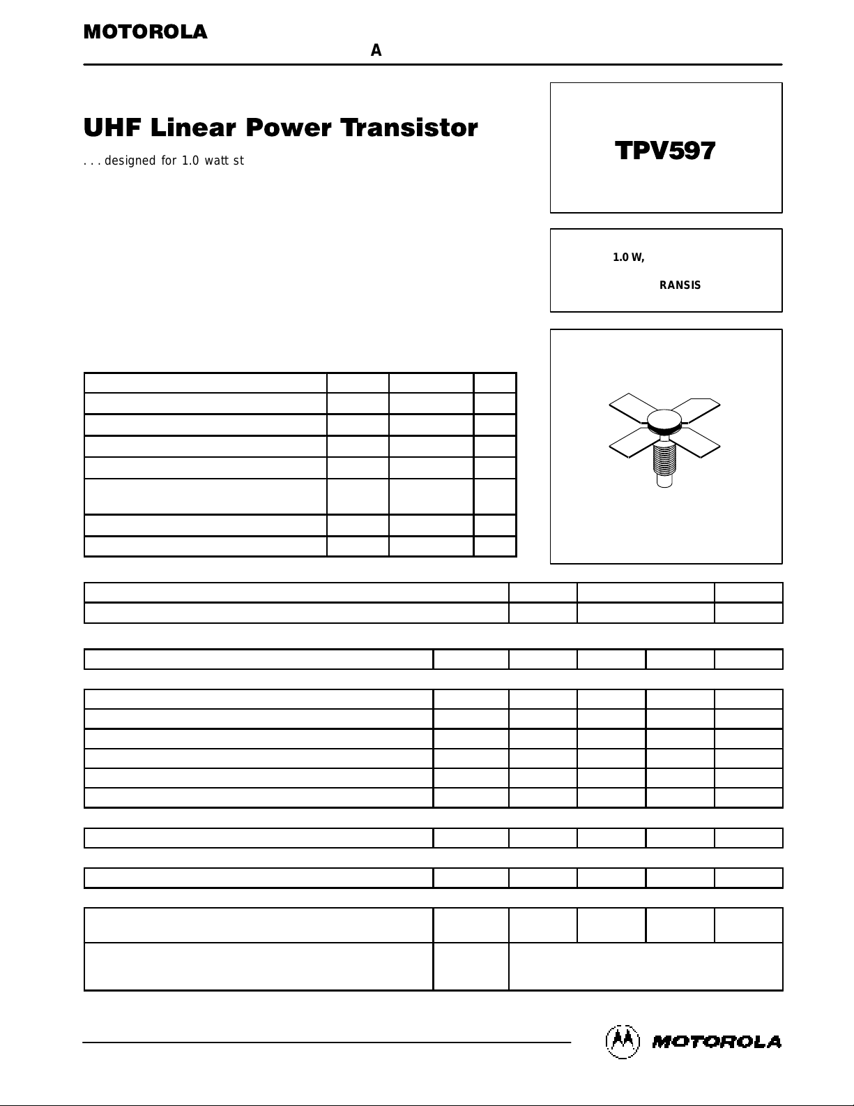
CASE 244–04, STYLE 1
(.280 SOE)
Motorola, Inc. 1994
Page 2
TPV597
2
MOTOROLA RF DEVICE DATA
ELECTRICAL CHARACTERISTICS — continued
Characteristic UnitMaxTypMinSymbol
FUNCTIONAL TESTS (continued)
Intermodulation Distortion, 3 Tone
(f = 860 MHz, VCE = 20 V, IE = 0.44 A, P
ref
= 1.0 W,
Vision Carrier = –8.0 dB, Sound Carrier = –7.0 dB,
Sideband Signal = –16 dB, Specification TV05001)
IMD
1
— –60 –58 dB
Cutoff Frequency (VCE = 20 V, IE = 0.44 A) f
τ
2.2 2.5 — GHz
Intermodulation Distortion (IDEM)
(f = 860 MHz, VCE = 20 V, IE = 0.44 A, P
ref
= 2.0 W,
Vision Carrier = –8.0 dB, Sound Carrier = –10 dB,
Sideband Signal = –16 dB)
IMD
2
— —
–ā51
dB
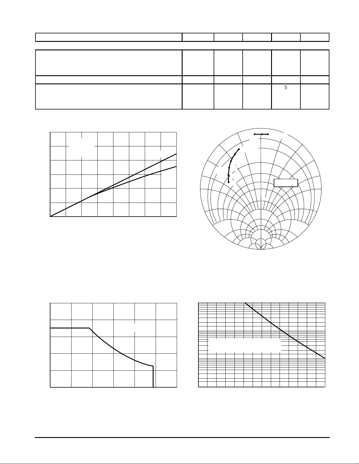
Figure 1. Power Output versus Power Input
Figure 2. Large Signal Impedances
VCE = 20 V — IC = 440 mA
Figure 3. Safe Operating Area Figure 4. MTTF Factor versus Junction
Temperature
ZOL* = Conjugate of the optimum load impedance into which the
device output operates at a given output power, voltage and
frequency.
0
0.2
0.4
0.6
0.8
1
1.5
2
3
4
5
10
0
10
5
3
4
1.5
2
1
0.8
0.6
0.4
0.2
0.1
0.2
0.4
0.6
0.8
1
1.5
2
3
4
5
10
f = 1 GHz
Z
in
0.9
f = 1 GHz
ZOL*
0.8
0.7
0.6
0.5
0.5
0.8
P , OUTPUT POWER (WATTS)
out
Pin, INPUT POWER (mW)
6
40 80 120
f = 860 MHz
VCE = 20 V
IC = 440 mA
IDEAL
REAL
5
4
3
2
1
160 200 240 280 320
I
C
, COLLECTOR CURRENT (A)
0
VCE, COLLECTOR–EMITTER VOLTAGE (VOLTS)
2
T
HEATSINK
= 70°C
1.6
1.2
0.8
0.4
5 10 15 20 25 30
MTTF FACTOR (10
2
)
6
HRS x AMP
100
TJ, JUNCTION TEMPERATURE (°C)
120 140 160 180 200
1
80
0.1
0.01
0.001
NOTE: DIVIDE MTTF FACTORY BY I
C
2
TO OBTAIN METAL LIFE
Zo = 50
Ω
Page 3

3
TPV597MOTOROLA RF DEVICE DATA
Figure 5. 860 MHz Test Circuit
Figure 6. Class A Bias Circuit
V
SUPPLY
R4
R1
R2
R3
R5
2N2904
V
BIAS
V
CE
1N4007
C
C — 100 µF + 10 nF + 1.0 nF
R1 — 1.0 kohm
R2 — 330 ohm
R3 — 4.7 kohm
R4 — 5.6 ohm 1/2 W
R5 — 390 ohm
V
BIAS
V
CE
C
L
220 pF
0.8–15 pF
50
Ω
50
Ω
0.8–10 pF
220 pF
220 pF
C
C
L
50
Ω
50
Ω
2% λg
7% g
λ
10% λg
L = 6 turns ID = 1 mm Wire diameter = 0.6 mm
The lengths are given for f = 860 MHz
NOTE:lg is the wave length in the microstrip circuit
Page 4

TPV597
4
MOTOROLA RF DEVICE DATA
PACKAGE DIMENSIONS
CASE 244–04
ISSUE J
STYLE 1:
PIN 1. EMITTER
2. BASE
3. EMITTER
4. COLLECTOR
K
D
A
J
T
F
P
M
2
13
4
SEATING PLANE
8–32 NC 2A
WRENCH FLAT
U
E
B
S
C
DIM MIN MAX MIN MAX
INCHESMILLIMETERS
A 7.06 7.26 0.278 0.286
B 6.20 6.50 0.244 0.256
C 14.99 16.51 0.590 0.650
D 5.46 5.96 0.215 0.235
E 1.40 1.65 0.055 0.065
G 1.52 ––– 0.060 –––
J 0.08 0.17 0.003 0.007
K 11.05 ––– 0.435 –––
M 45 NOM 45 NOM
P ––– 1.27 ––– 0.050
S 3.00 3.25 0.118 0.128
T 1.40 1.77 0.055 0.070
U 2.92 3.68 0.115 0.145
_ _
Motorola reserves the right to make changes without further notice to any products herein. Motorola makes no warranty, representation or guarantee regarding
the suitability of its products for any particular purpose, nor does Motorola assume any liability arising out of the application or use of any product or circuit,
and specifically disclaims any and all liability, including without limitation consequential or incidental damages. “T ypical” parameters can and do vary in different
applications. All operating parameters, including “T ypicals” must be validated for each customer application by customer’s technical experts. Motorola does
not convey any license under its patent rights nor the rights of others. Motorola products are not designed, intended, or authorized for use as components in
systems intended for surgical implant into the body, or other applications intended to support or sustain life, or for any other application in which the failure of
the Motorola product could create a situation where personal injury or death may occur. Should Buyer purchase or use Motorola products for any such
unintended or unauthorized application, Buyer shall indemnify and hold Motorola and its officers, employees, subsidiaries, affiliates, and distributors harmless
against all claims, costs, damages, and expenses, and reasonable attorney fees arising out of, directly or indirectly, any claim of personal injury or death
associated with such unintended or unauthorized use, even if such claim alleges that Motorola was negligent regarding the design or manufacture of the part.
Motorola and are registered trademarks of Motorola, Inc. Motorola, Inc. is an Equal Opportunity/Affirmative Action Employer.
How to reach us:
USA /EUROPE: Motorola Literature Distribution; JAPAN: Nippon Motorola Ltd.; Tatsumi–SPD–JLDC, Toshikatsu Otsuki,
P.O. Box 20912; Phoenix, Arizona 85036. 1–800–441–2447 6F Seibu–Butsuryu–Center, 3–14–2 Tatsumi Koto–Ku, Tokyo 135, Japan. 03–3521–8315
MFAX: RMFAX0@email.sps.mot.com – TOUCHTONE (602) 244–6609 HONG KONG: Motorola Semiconductors H.K. Ltd.; 8B Tai Ping Industrial Park,
INTERNET: http://Design–NET.com 51 Ting Kok Road, Tai Po, N.T., Hong Kong. 852–26629298
TPV597/D
*TPV597/D*
◊
 Loading...