

Page 1
T
TPS9125
5 V/3 V SIM SUPPLY AND LEVEL SHIFTERS
SLVS244A – SEPTEMBER 1999 – REVISED NOVEMBER 1999
D
Integrated SIM Supply and Level Shifters
D
Selectable 5-V or 3-V SIM Supply Voltage
D
3-V to 5-V Level Shifters, Bidirectional for
SIM Data Line
D
10 kV ESD Protection (HBM) on SIMDATA,
SIMRST, and SIMCLK Terminal
D
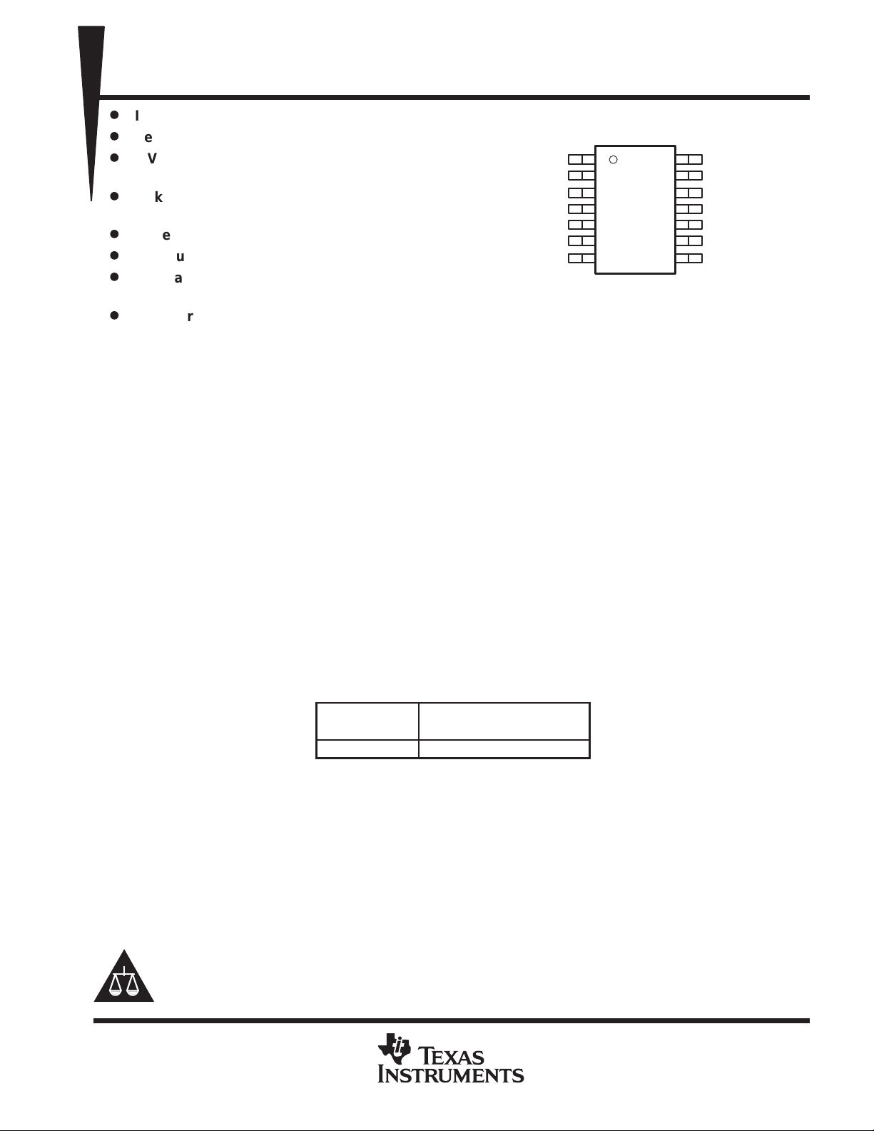
14 Terminal TSSOP
D
Minimum Supply Voltage 2.7 V
D
Integrated PullUp Resistor for DATA and
V
DD
RESET
MODE
SIMPWR
DATA
CLK
RST
PW PACKAGE
(TOP VIEW)
1
2
3
4
5
6
7
14
13
12
11
10
9
8
SIMVCC
VCAP1
VCAP2
SIMDATA
GND
SIMCLK
SIMRST
SIMDATA
D
Thin Shrink, Small Outline, Left-Hand Tape
and Reel Package
description
The TPS9125 SIM supply and level shifter integrates a programmable 3-V or 5-V SIM supply , conformable to
the (GSM) test specification 11.10, together with either a 3-V or 5-V level shifter, conformable to the GSM
specification 11.11 and 11.12.
A charge pump, utilizing two external capacitors, is configured as voltage doubler to generate a 5-V supply rail
from VDD. Dependent on the SIM card used, a control signal coming from the SIM card controller is applied on
the MODE terminal to switch between a 3-V or 5-V supply on the SIMVCC output terminal.
A 3-V/5-V bidirectional level shifter translates the 3-V compatible logic signal on DATA terminal into a 5-V
compatible logic signal SIMDATA terminal, and vice versa. RST and CLK are unidirectional level shifters,
providing a 5-V SIMRST and SIMCLK signal from the microcontroller to the SIM card.
The SIM supply is operating provided SIMPWR = 1 and VDD is sufficient (> 2.7 V). Under this condition, SIMVCC
voltage is generated by the SIM supply charge pump.
A RESET terminal is provided for security reasons to switch off the SIM supply and interface if the SIM card is
disconnected or removed by accident.
The TSP9125 is packaged in TI’s thin shrink small-outline package (PW).
AVAILABLE OPTIONS
A
–30°C to 85°C TSP9125PWR
†
Suffix R stands for left-handed tape and reel.
Please be aware that an important notice concerning availability, standard warranty, and use in critical applications of
Texas Instruments semiconductor products and disclaimers thereto appears at the end of this data sheet.
PACKAGE
(PW)
†
TI is a trademark of Texas Instruments Incorporated.
PRODUCTION DATA information is current as of publication date.
Products conform to specifications per the terms of Texas Instruments
standard warranty. Production processing does not necessarily include
testing of all parameters.
POST OFFICE BOX 655303 • DALLAS, TEXAS 75265
Copyright 1999, Texas Instruments Incorporated
1
Page 2
TPS9125
I/O
DESCRIPTION
5 V/3 V SIM SUPPLY AND LEVEL SHIFTERS
SLVS244A – SEPTEMBER 1999 – REVISED NOVEMBER 1999
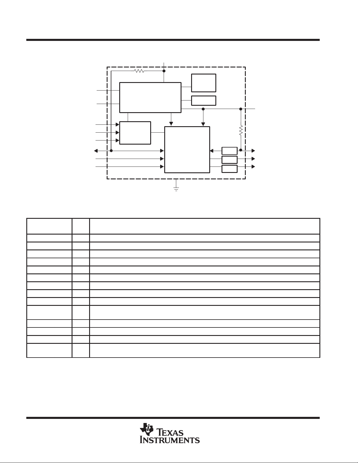
functional block diagram
V
DD
VCAP1
VCAP2
SIMPWR
MODE
RESET
DATA
CLK
RST
20 kΩ
Voltage
Generator
(Charge Pump)
Control
Control
Block
Block
Shifter
VDD or
SIMVCC
Level
GND
OSC
800 kHz
VREF
10 kΩ
ESD
ESD
ESD
SIMVCC
SIMDATA
SIMCLK
SIMRST
Terminal Functions
TERMINAL
NAME NO.
CLK 6 DI 3-V SIM clock signal. This terminal is connected to the SIM interface and works with 3-V logic level.
DATA 5 DI/O 3-V bidirectional data line. This terminal is connected to the SIM interface and works with 3-V logic level.
GND 10 Ground
MODE 3 DI Programs the SIM supply voltage to SIMVCC = 5 V (MODE = 0) or SIMVCC = 3 V (MODE = 1).
RESET 2 DI Reset for the TSP9125 SIM supply and interface in case the SIM is removed under operation.
RST 7 DI 3-V SIM reset signal. This terminal is connected to the SIM interface and works with 3-V logic level.
SIMCLK 9 DO 3-V/5-V SIM clock signal. This terminal is connected to the SIM reader contacts.
SIMRST 8 DO 3-V/5-V SIM reset signal. This terminal is connected to the SIM reader contacts.
SIMDATA 11 DI/O 3-V/5-V bidirectional data line. This terminal is connected to the SIM reader contacts.
SIMVCC 14
SIMPWR 4 DI SIM supply enable terminal. SIMPWR = 0 leaves SIMVCC open, SIMPWR = 1 enables SIM supply.
VCAP1 13 Charge pump capacitor. Connect 220 nF ±20% capacitor between VCAP1 and VCAP2.
VCAP2 12 Charge pump capacitor. Connect 220 nF ±20% capacitor between VCAP1 and VCAP2.
V
DD
1
SIM supply voltage. Can be switched between 5 V ±10% and 3 V ±10%. This terminal is connected to the SIM
reader contacts. Connect a 1 µF ±20% capacitor between SIMVCC and GND.
Supply voltage input. Connect a power bypass capacitor of 1 µF between VDD and GND. Connect capacitor
physically close to the VDD terminal.
2
POST OFFICE BOX 655303 • DALLAS, TEXAS 75265
Page 3
5 V/3 V SIM SUPPLY AND LEVEL SHIFTERS
SLVS244A – SEPTEMBER 1999 – REVISED NOVEMBER 1999
detailed description
voltage generator (charge pump)
The voltage generator can be programmed in two modes:
1. SIMPWR = 0: SIMVCC is left open, voltage generator disabled.
2. SIMPWR = 1: Depending on the signal on control terminal MODE, SIMVCC is either programmed to:
a. MODE = 0: 5 V ±10% (this is the default condition under which the system powers up),
or
b. MODE = 1: SIMV
The setting of the SIMVCC voltage (MODE = 0 or 1) can only be changed when SIMPWR is low. Therefore, as
specified in GSM11.12, supply voltage switching is performed by deactivating the SIM and activating it at the
new supply voltage.
In 5-V mode, a regulated charge pump is used to step-up the 3-V supply rail (min 2.7 V) to the 5-V supply rail.
The voltage generator uses two external capacitors, one pump capacitor connected between VCAP1 and
VCAP2 and one output buffer capacitor connected between SIMVCC and GND. It operates at a nominal
frequency of 800 kHz, and also supplies the integrated level shifters to allow for 5-V compatible logic signals
on SIMRST, SIMCLK, and SIMDATA.
is equal to the supply voltage VDD minus a voltage drop of 50 mV maximum.
CC
TPS9125
In 3-V mode, the supply voltage VDD is connected via an integrated PMOS switch to the SIMVCC output. The
charge pump, oscillator, and voltage reference are disabled in the 3-V mode to reduce power consumption. The
supply voltage of the integrated level shifters is V
minus a voltage drop of 50 mV maximum.
DD
control block
The control block uses the three control signals SIMPWR, MODE, and RESET to set the TSP9125 operation
modes.
When SIMPWR is set low, the TSP9125 goes to power-down mode. To comply with the ISO/IEC 7816-3
specification for deactivation of the SIM contacts, the input terminals RST, DA TA, and CLK must be low before
the SIMPWR terminal is allowed to be taken low. When SIMPWR is low, the SIMRST, SIMDA TA, and SIMCLK
terminals are kept low and SIMVCC is left open.
The RESET input is used to disable the TSP9125 in case the SIM card is removed from the reader under
operation. The input is therefore typically connected to a mechanical or other device used to detect the removal
of the SIM card. When RESET is taken low, the SIMDAT A, SIMCLK, and SIMRST terminals are taken low and
SIMVCC is left open, until RESET is taken high again.
Table 1. Control Block Function Table
RESET MODE SIMPWR OPERATING MODE
0 X X SIM supply disabled; SIMVCC open; SIMRST and SIMCLK and SIMDATA low
1 0 0 TSP9125 in power-down mode. SIM supply disabled; SIMVCC open; SIMRST, SIMCLK, and SIMDA T A low;
1 1 0 TSP9125 in power-down mode. SIM supply disabled; SIMVCC open; SIMRST, SIMCLK, and SIMDA T A low;
1 X 1 TSP9125 in normal operation mode; SIM supply enabled, SIMVCC = 5 V or 3 V depending on how it was
SIMVCC programmed to 5-V mode.
SIMVCC programmed to 3-V mode.
programmed.
POST OFFICE BOX 655303 • DALLAS, TEXAS 75265
3
Page 4
TPS9125
5 V/3 V SIM SUPPLY AND LEVEL SHIFTERS
SLVS244A – SEPTEMBER 1999 – REVISED NOVEMBER 1999
detailed description (continued)
level shifters
The level shifters on TSP9125, when operating in the 5-V mode, convert a 3-V compatible logic signal from a
digital control chip (SIM Controller) into a 5-V compatible logic signal for the SIM Card.
Operating in the 3-V mode, the level shifters are disabled and only pass the signal through.
The level shifters for reset and clock signal are unidirectional (RST to SIMRST, CLK to SIMCLK). The level
shifter for the data signal is bidirectional, enabling signal exchange in both directions (DA TA to SIMDATA and
SIMDATA to DATA).
During power up and power down of the TSP9125, the voltage level on the SIMRST, SIMCLK, and SIMDAT A
terminals is kept below 0.4 V for currents less than 1 mA flowing into the TSP9125, provided VDD is applied.
pullup resistors
The DA TA and SIMDATA I/O pullup resistors are integrated in the device. The DATA resistor is 20 kΩ and the
SIMDATA resistor is 10 kΩ.
oscillator
An integrated RC oscillator provides the charge pump with a nominal clock frequency of 800 kHz.
voltage reference
An integrated bandgap reference provides a reference voltage of 1.192 V to the charge pump to control and
regulate the output voltage.
ESD protection
In a cellular telephone (GSM phone) the SIMRST, SIMCLK, and SIMDA TA terminals are connected directly to
the contacts of the SIM reader. This means they are accessible from the outside and therefore require increased
ESD protection. The terminals withstand 10 kV ESD when tested according to human body model (HBM),
100 pF through 1500 Ω.
DISSIPATION RATING TABLE
PACKAGED
PW 556 mW 5.56 mW/°C 306 mW
TA < 25°C
POWER RATING
OPERATING FACTOR
ABOVE TA = 25°C
TA = 70°C
POWER RATING
4
POST OFFICE BOX 655303 • DALLAS, TEXAS 75265
Page 5
TPS9125
5 V/3 V SIM SUPPLY AND LEVEL SHIFTERS
SLVS244A – SEPTEMBER 1999 – REVISED NOVEMBER 1999
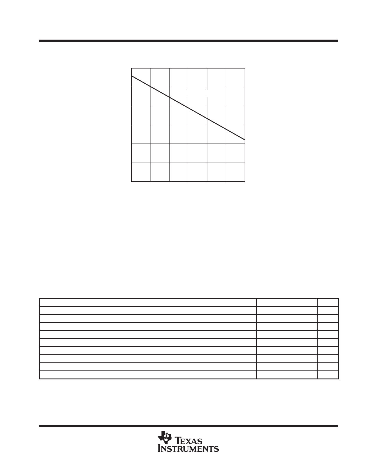
DISSIPATION DERATING CURVE
vs
FREE-AIR TEMPERATURE
6
5
RthJA – 180°C/W
4
3
2
Power Dissipation – mW
1
0
25 35 45 55
TA – Free-Air Temperature – °C
absolute maximum ratings over operating free-air temperature (unless otherwise noted)
65 75 85
†
Supply voltage range, VDD –0.3V to 4 V. . . . . . . . . . . . . . . . . . . . . . . . . . . . . . . . . . . . . . . . . . . . . . . . . . . . . . . . . . .
Input voltage range, all other terminals –0.3V to V
DD
+ 0.3V. . . . . . . . . . . . . . . . . . . . . . . . . . . . . . . . . . . . . . . . .
Peak output current, SIMVCC 20 mA. . . . . . . . . . . . . . . . . . . . . . . . . . . . . . . . . . . . . . . . . . . . . . . . . . . . . . . . . . . . . .
Free-air temperature range –40°C to 85°C. . . . . . . . . . . . . . . . . . . . . . . . . . . . . . . . . . . . . . . . . . . . . . . . . . . . . . . . .
Storage temperature range –60°C to 125°C. . . . . . . . . . . . . . . . . . . . . . . . . . . . . . . . . . . . . . . . . . . . . . . . . . . . . . . .
Continuous total power dissipation 0.1 W. . . . . . . . . . . . . . . . . . . . . . . . . . . . . . . . . . . . . . . . . . . . . . . . . . . . . . . . . .
†
Stresses beyond those listed under “absolute maximum ratings” may cause permanent damage to the device. These are stress ratings only, and
functional operation of the device at these or any other conditions beyond those indicated under “recommended operating conditions” is not
implied. Exposure to absolute-maximum-rated conditions for extended periods may affect device reliability.
recommended operating conditions
MIN NOM MAX UNIT
Supply voltage, V
Charge pump capacitor between VCAP1 and VCAP2 220 nF
Charge pump output capacitor on SIMVCC 1 µF
Input capacitor on VDD 0.1 1 µF
Operating free-air temperature range –30 85 °C
Operating virtual junction temperature range –30 125 °C
ESD susceptibility kV
SIMRST, SIMCLK, SIMDATA (human body model, 100 pF through 1500 Ω) 10 (TBC) kV
All other terminals (human body model, 100 pF through 1500 Ω) 2
DD
2.7 3 3.3 V
POST OFFICE BOX 655303 • DALLAS, TEXAS 75265
5
Page 6
TPS9125
Clock frequency CLK/SIMCLK
MH
5 V/3 V SIM SUPPLY AND LEVEL SHIFTERS
SLVS244A – SEPTEMBER 1999 – REVISED NOVEMBER 1999
electrical characteristics over recommended operating junction temperature range, VDD = 3 V,
C
VCAP1/2
= 220 nF ±20%; C
SIMVCC
voltage generator charge pump (SIMVCC)
PARAMETER TEST CONDITIONS MIN TYP MAX UNIT
Output voltage at SIMVCC, 5-V mode
Output voltage at SIMVCC, 3-V mode
Output current at SIMVCC, 5-V mode
(see Note 1)
Output current at SIMVCC, 3-V mode
(see Note 1)
Switching frequency (internal oscillator
frequency)
Output ripple 5-V mode, I
Startup time Standby to 5-V mode 1 ms
Power efficiency I
NOTE 1: The SIM supply circuit is designed according to the GSM specification 11.11 and 1 1.12 and complies to the requirements of GSM test
specification 11.10. For more information, please see application section.
2.7 V < VDD < 3.3 V,
f
2.7 V < VDD < 3.3 V,
MODE = 1
2.7 V < VDD < 3.3 V 10 mA
2.7 V < VDD < 3.3 V 6 MA
= 1 µF ±20%; SIMPWR = 1 (unless otherwise noted)
SIMCLK
SIMVCC
I
= 0 MHz,
= 10 mA 82.5%
SIMVCC
MODE = 0 (default value)
I
SIMVCC
out
= 10 mA,
= 6 mA,
= 10 mA 100 mV
4.5 5.5 V
VDD–50 mV VDD–50 mV V
440 800 1 160 kHz
level shifters (see Note 2)
PARAMETER TEST CONDITIONS MIN TYP MAX UNIT
5-V mode 1 5
3-V mode 1 4
Clock duty cycle on SIMCLK
Output load, driver side 70 100 pF
Data rate on DATA/SIMDA TA Clk/372 Clk/32 MHz
Residual voltage at SIMRST, SIMCLK, SIMDATA in powerdown mode SIMPWR = 0, I = 8 µA –0.4 0.4 V
NOTE 2: The level shifters are designed according to the GSM specification 11.11 and 11.12.
5-V mode and 3-V mode,
CLK input 50% duty cycle
40% 50% 60%
logic inputs (CLK, MODE, RESET, RST, SIMPWR) (see Note 3)
PARAMETER TEST CONDITIONS MIN TYP MAX UNIT
V
High-level input voltage 0.7×V
IH
V
Low-level input voltage 0.3×V
IL
Input capacitance 10 pF
Input current –20 –10 1
Input leakage current VIN = 0.5 V to 3 V –1 1
NOTE 3: For each state VIH, VIL, a positive current is defined as flowing out of the TSP9125.
DD
DD
logic output SIMCLK in 3-V mode (according to GSM 11.12) (see Note 4)
PARAMETER TEST CONDITIONS MIN TYP MAX UNIT
V
High-level output voltage I
OH
Low-level output voltage I
Rise/fall time SIMCLK (see Note 5) Cin = C
NOTES: 4. For each state VOH, VOL, a positive current is defined as flowing out of the TSP9125.
5. T o allow for overshoot the voltage on SIMCLK should remain between –0.3 V and SIMVCC+0.3 V during dynamic operations.
= 20 µA 0.7×SIMV
OHmax
= –20 µA 0 0.2×SIMV
OLmax
= 100 pF 50 ns
out
CC
SIMV
CC
CC
z
V
V
V
V
6
POST OFFICE BOX 655303 • DALLAS, TEXAS 75265
Page 7
TPS9125
5 V/3 V SIM SUPPLY AND LEVEL SHIFTERS
SLVS244A – SEPTEMBER 1999 – REVISED NOVEMBER 1999
electrical characteristics over recommended operating junction temperature range, VDD = 3 V,
C
VCAP1/2
= 220 nF ±20%; C
SIMVCC
logic output SIMCLK in 5-V mode (according to GSM 11.11)
PARAMETER TEST CONDITIONS MIN TYP MAX UNIT
V
High-level output voltage (see Note 4) I
OH
V
Low-level output voltage (see Note 4) I
OL
tr/tfRise/fall time SIMCLK (see Note 5 and 6) Cin = C
NOTES: 4. For each state VOH, VOL, a positive current is defined as flowing out of the TSP9125.
5. T o allow for overshoot the voltage on SIMCLK should remain between –0.3 V and SIMVCC+0.3 V during dynamic operations.
6. The maximum rise/fall time is 9% of the SIMCLK period.
logic output SIMRST in 3-V mode (according to GSM 11.12)
PARAMETER TEST CONDITIONS MIN TYP MAX UNIT
V
High-level output voltage (see Note 4) I
OH
V
Low-level output voltage (see Note 4) I
OL
tr/tfRise/fall time SIMRST (see Note 5) Cin = C
NOTES: 4. For each state VOH, VOL, a positive current is defined as flowing out of the TSP9125.
5. T o allow for overshoot the voltage on SIMCLK should remain between –0.3 V and SIMVCC+0.3 V during dynamic operations.
= 1 µF ±20%; SIMPWR = 1 (unless otherwise noted) (continued)
= 20 µA 0.7×SIMV
OHmax
= –200 µA 0 0.5 V
OLmax
= 100 pF, f
out
= 200 µA 0.8×SIMV
OHmax
= –200 µA 0 0.2×SIMV
OLmax
= 100 pF 400 µs
out
= 5 MHz 18 ns
SIMCLK
CC
CC
SIMV
SIMV
CC
CC
CC
V
V
V
logic output SIMRST in 5-V mode (according to GSM 11.11)
PARAMETER TEST CONDITIONS MIN TYP MAX UNIT
V
High-level output voltage (see Note 4) I
OH
V
Low-level output voltage (see Note 4) I
OL
tr/tfRise/fall time SIMRST (see Note 5) Cin = C
NOTES: 4. For each state VOH, VOL, a positive current is defined as flowing out of the TSP9125.
5. T o allow for overshoot the voltage on SIMCLK should remain between –0.3 V and SIMVCC+0.3 V during dynamic operations.
= 200 µA SIMVCC–0.7V SIMV
OHmax
= –200 µA 0 0.6 V
OLmax
= 100 pF 400 µs
out
CC
V
logic input/output DATA
PARAMETER TEST CONDITIONS MIN TYP MAX UNIT
V
High-level input voltage on DATA (see Note 7) 0.7×V
IH
V
Low-level input voltage on DATA (see Note 7) 0.2×V
IL
V
High-level output voltage on DATA (see Note 7) I
OH
V
Low-level output voltage on DATA (see Note 7) I
OL
tr/tfRise/fall time DA TA (see Note 5)
NOTES: 5. To allow for overshoot the voltage on SIMCLK should remain between –0.3 V and SIMVCC+0.3 V during dynamic operations.
7. For each state VOH, VOL, VIH, VIL, a positive current is defined as flowing out of the TSP9125.
Cin = C
Integrated pullup resistor = 20 kΩ
OHmax
OLmax
= 20 µA, V
= –1 mA, V
= 100 pF,
out
SIMDATA
SIMDATA
= 3 V 0.7×V
= 0 V 0 0.4 V
DD
DD
DD
V
DD
1 µs
V
V
V
POST OFFICE BOX 655303 • DALLAS, TEXAS 75265
7
Page 8
TPS9125
Ground current, operating
A
5 V/3 V SIM SUPPLY AND LEVEL SHIFTERS
SLVS244A – SEPTEMBER 1999 – REVISED NOVEMBER 1999
electrical characteristics over recommended operating junction temperature range, VDD = 3 V,
C
VCAP1/2
= 220 nF ±20%; C
SIMVCC
logic input/output SIMDATA in 3-V mode (according to GSM 11.12)
PARAMETER TEST CONDITIONS MIN TYP MAX UNIT
High-level input voltage on SIMDATA
V
IH
(see Note 7)
Low-level input voltage on SIMDATA (see
V
IL
Note 7)
High-level output voltage on SIMDATA
V
OH
(see Note 7)
Low-level output voltage on SIMDATA
V
OL
(see Note 7)
tr/tfRise/fall time SIMRST (see Note 5)
NOTES: 5. To allow for overshoot the voltage on SIMCLK should remain between –0.3 V and SIMVCC+0.3 V during dynamic operations.
7. For each state VOH, VOL, VIH, VIL, a positive current is defined as flowing out of the TSP9125.
logic input/output SIMDATA in 5-V mode (according to GSM 11.12)
PARAMETER TEST CONDITIONS MIN TYP MAX UNIT
High-level input voltage on SIMDATA (see
V
IH
Note 7)
Low-level input voltage on SIMDATA (see
V
IL
Note 7)
High-level output voltage on SIMDATA
V
OH
(see Note 7)
Low-level output voltage on SIMDATA
V
OL
(see Note 7)
tr/tfRise/fall time SIMRST (see Note 5)
NOTES: 5. To allow for overshoot the voltage on SIMCLK should remain between –0.3 V and SIMVCC+0.3 V during dynamic operations.
7. For each state VOH, VOL, VIH, VIL, a positive current is defined as flowing out of the TSP9125.
= 1 µF ±20%; SIMPWR = 1 (unless otherwise noted) (continued)
I
= ±20 µA 0.7×SIMV
IHmax
I
= 1 mA –0.3 0.2×SIMV
ILmax
I
= 20 µA, V
OHmax
I
= –1 mA, V
OLmax
Cin = C
Integrated pullup resistor = 10 kΩ
I
IHmax
I
ILmax
I
OHmax
I
OLmax
Cin = C
Integrated pullup resistor = 10 kΩ
= 100 pF,
out
= ±20 µA 0.7×SIMV
= 1 mA –0.3 0.8 V
= 20 µA, V
= –1 mA, V
= 100 pF,
out
= 3 V 0.7×SIMV
DATA
= 0 V 0 0.4 V
DATA
= 3 V 0.7×SIMV
DATA
= 0 V 0 0.4 V
DATA
CC
CC
CC
CC
SIMVCC+0.3V V
CC
SIMV
CC
1 µs
SIMVCC+0.3V V
SIMV
CC
1 µs
V
V
V
supply current
PARAMETER TEST CONDITIONS MIN TYP MAX UNIT
Powerdown/programming mode SIMPWR = 0 5 µA
SIMVCC = 5 V, I
p
SIMVCC = 5 V, I
SIMVCC = 3 V, I
SIMVCC = 3 V, I
SIMVCC
SIMVCC
SIMVCC
SIMVCC
= 0 mA 125
= 10 mA 200
= 0 mA 25
= 6 mA 40
µ
8
POST OFFICE BOX 655303 • DALLAS, TEXAS 75265
Page 9

5 V/3 V SIM SUPPLY AND LEVEL SHIFTERS
SLVS244A – SEPTEMBER 1999 – REVISED NOVEMBER 1999
PARAMETER MEASUREMENT INFORMATION
Colck Cycle
SIMVCC
50% 50%
GND
Figure 1. Clock Duty Cycle Measurment Figure 2. Rise and Fall Time Measurment
Fall Time Rise Time
TPS9125
ME
I = NEGATIVE
I = POSITIVE I = NEGATIVE
TPS9215 SIM
I = POSITIVE
Figure 3. Current Direction Convention
VDD = 3 V
Input Bypass Capacitor
C1 = 220 nF
SIM Card
Inserted
C3 = 1 µF
1
12
4
3
2
VCAP1
VCAP2
SIMPWR
MODE
RESET
RESET
1
VDD
SIMVCC
14
C2 =
1 µF
RO =
500 Ω
5
DATA
6
CLK
7
RST
10
SIMDATA
SIMCLK
SIMRST
GND
Figure 4. Parameter Measurment Information
POST OFFICE BOX 655303 • DALLAS, TEXAS 75265
11
9
8
9
Page 10

TPS9125
5 V/3 V SIM SUPPLY AND LEVEL SHIFTERS
SLVS244A – SEPTEMBER 1999 – REVISED NOVEMBER 1999
PARAMETER MEASUREMENT INFORMATION
VDD = 3 V
VDD
µC I/O max.
CI = 30 pF
20 kΩ
Transfer
5
Gate
DATA
GND
1
VDD
10
SIMVCC
10 kΩ
SIMDATA
14
11
SIMVCC = 5 V
VCC
Figure 5. Parameter Measurment Information SIMDA TA
The rise and fall time on DATA and SIMDATA signals depend on the I/O parameters of the used hardware
(microcontroller and SIM card).
TYPICAL CHARACTERISTICS
Table of Graphs
FIGURE
SIMV
Charge pump power loss vs Output current on SIMV
Charge pump power efficiency vs Output current on SIMV
Charge pump power efficiency vs Supply voltage V
Charge pump performance vs Supply voltage V
CC
CC
CC
DD
DD
6
7
8
9
10
POST OFFICE BOX 655303 • DALLAS, TEXAS 75265
Page 11

TPS9125
5 V/3 V SIM SUPPLY AND LEVEL SHIFTERS
SLVS244A – SEPTEMBER 1999 – REVISED NOVEMBER 1999
TYPICAL CHARACTERISTICS
POWER LOSS
CURRENT LOAD
20
18
16
14
12
10
8
Power Loss – mW
6
4
2
0
T = 27°C
Nominal Models
C
= 220 nF
pump
C
= 1 µF
sim
VDD = 3 V
0123456
POWER EFFIENCY
SUPPLY VOLTAGE
90
85
vs
Charge Pump
Theoretical Limit
L
– mA
load
Figure 6
vs
Theoretical Limit
78910
POWER EFFICIENCY
CURRENT LOAD
90
85
80
Power Efficiency – %
75
70
0123456
5V OUTPUT STARTUP
SUPPLY VOLTAGE
5.5
SIMVCC = 1 µF
C
= 220 nF
pump
L
= 10 mA
load
TA = –40°C
5
vs
Theoretical Limit
T = 27°C
Nominal Models
C
C
VDD = 3 V
L
– mA
load
Figure 7
vs
Charge Pump
= 220 nF
pump
= 1 µF
sim
78910
Charge Pump
80
Power Efficiency – %
T = 27°C
75
Nominal Models
C
= 220 nF
pump
C
= 1 µF
sim
IO = 10 mA
70
2.5 2.6 2.7 2.8 2.9 3 3.1
VDD Supply Voltage - V
Figure 8
4.5
5V Output Startup – V
4
3.2 3.3 3.4 3.5
POST OFFICE BOX 655303 • DALLAS, TEXAS 75265
2.5 2.6 2.7 2.8 2.9 3 3.1
TA = 27°C
TA = 100°C
3.2 3.3 3.4 3.5
VDD Supply Voltage - V
Figure 9
11
Page 12

TPS9125
5 V/3 V SIM SUPPLY AND LEVEL SHIFTERS
SLVS244A – SEPTEMBER 1999 – REVISED NOVEMBER 1999
THERMAL INFORMATION
Implementation of integrated circuits in low profile and fine-pitch surface-mount packages requires special
attention to power dissipation. Many system-dependent issues such as thermal coupling, airflow, added heat
sinks and convection surfaces, as well as the presence of other heat-generating components, affect the
power-dissipation limits of a given component.
Three basic approaches for enhancing thermal performance are listed below.
D
Improving the power dissipation capability of the PWB design
D
Improving the thermal coupling of the component to the PWB
D
Introducing airflow in the system
Using the given R
T
P
D(MAX)
+
J(MAX)
for this IC, the maximum power dissipation can be calculated with the equation:
θJA
*
T
A
R
Q
JA
5 V MODE SIMVCC OUTPUT
vs
FREE-AIR TEMPERATURE
5.040
5.035
5.030
5.025
5 V Mode SIMVCC Output – V
5.050
–10 01020304050
TA – Free-Air Temperature – °C
60 70 80 90
12
Figure 10
POST OFFICE BOX 655303 • DALLAS, TEXAS 75265
Page 13

5 V/3 V SIM SUPPLY AND LEVEL SHIFTERS
SLVS244A – SEPTEMBER 1999 – REVISED NOVEMBER 1999
APPLICATION INFORMATION
charge pump terminal
The charge pump can be used to generate a negative voltage from a positive supply voltage, or to
voltage-double, triple, or otherwise multiply the supply voltage. In the TSP9125, a charge pump is used to
generate a 5-V supply rail from an input voltage of 3 V.
Figure 11 is used to explain the principle of a charge pump when configured as a voltage doubler.
TPS9125
C1
S3
S4
GND
V
DD
SIMVCC
C2
V
DD
S1
S2
GND
OSC
1
VCAP1
VCAP2
Figure 11. Principal of a Charge Pump Configured as a Voltage Doubler
During the first half of the oscillator period, switches S1 and S2 are closed, switches S3 and S4 are open, and
the pump capacitor C1 is charged. In the second half of the oscillator period, switches S3 and S4 are closed
and switches S1 and S2 are open. Immediatetly after closing the switches S3 and S4, the voltage at Node 1
is:
V1+
VDD)
VC1≈ 2 V
DD
assuming C1 was charged up to VDD. In this half of the period, the pump capacitor C1 charges the output
capacitor C2. After the start-up time, the output capacitor C2 is charged up to
V
and the voltage at SIMVCC
1
is stable at this value, with only a small amount of ripple, which is normally around 1% of the supply voltage.
The ripple depends on the oscillator frequency, the load on SIMVCC, and the size of output capacitor C2.
In practice, the voltage V1 is a little bit less than 2 × VDD because of conduction losses across the switches and
switching losses in capacitor C1.
An unregulated charge pump generates an output voltage that is only dependent on the supply voltage and the
output current.
voltage generator
The charge pump used in the TSP9125 is regulated in such a way that the output voltage stays at 5 V ± 10%,
independently of the supply voltage and output current. A two-point regulator scheme was used to control the
output voltage. In addition, it reduces power consumption. The charge pump is active and enabled as long as
an oscillator frequency is applied. Figure 11 shows the functional block diagram of the voltage generator.
POST OFFICE BOX 655303 • DALLAS, TEXAS 75265
13
Page 14

TPS9125
5 V/3 V SIM SUPPLY AND LEVEL SHIFTERS
SLVS244A – SEPTEMBER 1999 – REVISED NOVEMBER 1999
APPLICATION INFORMATION
VCAP2 VCAP1
V
DD
C1
T1
MODE
OSC
TPS9125
Charge Pump
Control
Logic
Mode
VREF
1.192 V
T2
1
SIMPWR
SIMVCC
C2
GND
Figure 12. Functional Block Diagram of the Voltage Generator
When the TSP9125 is programmed in 5-V mode, the voltage at SIMVCC is monitored and regulated. If the
voltage of SIMVCC exceeds a defined upper threshold, the charge pump is switched off by disabling the
oscillator. In this state, all switching losses are zero, and the load is supplied only from the output capacitor C2.
The charge pump and oscillator are reactivated if the voltage at SIMVCC drops below a defined lower threshold.
In this state, the charge pump recharges output capacitor C2 until the voltage across C2 again exceeds the
defined upper threshold. Figure 12 shows the waveform of the charge pump output SIMVCC in 5-V mode.
Using this control mechanism, the switching losses of the charge pump and the losses of the oscillator are
minimized, because the charge pump and the oscillator are only activated when they are needed.
14
SIMVCC
Charge Pump
Enabled
Charge Pump
Disabled
Upper Threshold
Regulator
Hysteresis
max. 100 mV
Lower Threshold
Time
Figure 13. Typical Waveform at Charge Pump Output SIMVCC in 5-V Mode
POST OFFICE BOX 655303 • DALLAS, TEXAS 75265
Page 15

TPS9125
5 V/3 V SIM SUPPLY AND LEVEL SHIFTERS
SLVS244A – SEPTEMBER 1999 – REVISED NOVEMBER 1999
APPLICATION INFORMATION
VOLTAGE OUTPUT
vs
SIM CLOCK FREQUENCY
4.9
4.8
VDD = 3.3 V
4.7
4.6
4.5
4.4
Voltage Out – V
4.3
4.2
4.1
4
0 0.5 1 1.5 2 2.5 3
SIM Clock Frequency – MHz
VDD = 2.8 V
VDD = 2.7 V
3.5 4 4.5 5
Figure 14. Voltage At SIMVCC vs Frequency at SIMCLK Terminal in 5-V Mode
Figure 14 shows the output voltage on SIMVCC in 5-V mode versus the frequency of the clock signal on
CLK/SIMCLK dependent on the input voltage VDD. The load on the charge pump is the sum of the maximum
dc load on SIMVCC (10 mA) and the ac load of 100 pF on SIMCLK buffer.
In 3 V mode, the charge pump and oscillator are disabled all the time, thus reducing power dissipation to a
minimum. Switches T1 and T2 in Figure 14 directly connect the supply voltage on VDD to SIMVCC; the voltage
on SIMVCC is therefore equal to the supply voltage V
minus the conduction losses across the switches.
DD
dimensioning of the capacitors
output capacitor C2
The value of output capacitor C2 depends on the maximum charge pump load current, the allowed ripple on
SIMVCC, and the charge pump operating frequency.
In 5-V mode, the charge pump also supplies the drivers of the 5-V level shifters. The maximum load current the
charge pump has to provide is therefore the sum of the dc output current at SIMVCC and the ac supply current
for the level shifters; the SIMCLK driver is the major contributor to this ac load:
I
LOADmax
The minimum, theoretical required value for C2 can be calculated using the equation below:
C2
min
As described above, the regulated charge pump is disabled during the time in which the voltage across the
output capacitor C2 is above the lower threshold voltage, and therefore high enough to ensure the specified
minimum voltage on SIMVCC.
+
I
LOADmax
+
I
SIMVCCmax
V
ripple
)
I
ACmax
ƒ
+
V
ripple
+
10 mA)6mA+16 mA
I
LOADmax
2
POST OFFICE BOX 655303 • DALLAS, TEXAS 75265
ƒ
OSC
+
100 mV 2 440 kHz
16 mA
+
185 nF
15
Page 16

TPS9125
5 V/3 V SIM SUPPLY AND LEVEL SHIFTERS
SLVS244A – SEPTEMBER 1999 – REVISED NOVEMBER 1999
APPLICATION INFORMATION
output capacitor C2 (continued)
Increasing the value of the capacitor C2 will increase the time the charge pump is disabled. The power
consumption of the charge pump will be reduced, because the active time in which switching losses occur is
shorter. However, a larger value of C2 also results in a longer start-up time for the 5-V supply. Based on the
above considerations a 1 µF capacitor is recommended for C2.
pump capacitor C1
The value of pump capacitor C1 has a big impact on the start-up time of the charge pump: this is the time needed
to charge the output capacitor C2 from 0 V up to 5 V . The recommended value for capacitor C1 is 220 nF, thus
ensuring a start-up time of less than 1ms. If a lower value for capacitor C1 is chosen, the start-up time will
increase.
input capacitor
During the activation time of the charge pump there are steep current slopes of about 40 mA on the supply input
V
. Therefore, it is recommended to use a low ESR 1 µF capacitor, such as a multilayer ceramic or tantalum
DD
capacitor, on the VDD terminal.
capacitor selection
The exact capacitance value of the capacitors used is not as critical as the use of high quality and low ESR
(equivalent serial resistance) capacitors, such as multilayer ceramic or tantalum capacitors.
The ESR of C1 causes a voltage drop during charging and discharging, and this degrades the performance of
the charge pump. Low ESR is most critical for the choice of capacitor C1, because the charge current of this
capacitor is twice as much as the load current and the current through output capacitor C2. If a tantalum
capacitor is used for C1, the positive terminal should be connected to VCAP1.
The ESR of output capacitor C2 increases the ripple on SIMVCC. The ESR of C2 has only a minor influence,
because the ripple on SIMVCC in the TSP9125 is fixed at maximum 100 mV, due to the two-point regulation
scheme used. If a tantalum capacitor is used for C2, the positive terminal should be connected to SIMVCC.
pulsed output current
To comply with GSM test specification 11.10, paragraph 27.17.2.1.2, the SIMVCC supply voltage must stay
above the minimum allowed voltage level when spikes in the current consumption of the card occur. For a 5-V
SIM card interface, those spikes are up to a maximum charge of 40nAs. To test for this requirement, current
pulses of maximum 400 ns duration and maximum 200 mA amplitude are drawn from SIMVCC. For a 3-V SIM
card interface, those spikes are up to a maximum 12 mA charge. To test for this requirement, current pulses
of maximum 400ns duration and maximum 60-mA amplitude are drawn from SIMVCC.
In 5-V mode (MODE = 0), SIMV
Because the TSP9125 charge pump itself is too slow to counteract these peaks, the correct combination of
capacitors on SIMVCC must be chosen to cope with these requirements. In addition to the 1 µF ±20% low ESR
ceramic capacitor used to buffer the SIMVCC output, it is recommended to connect a 100 nF ceramic capacitor
as close as possible to the contacting elements.
must stay above 4.5 V , in 3-V mode (MODE = 1), it must stay above 2.7 V.
CC
16
POST OFFICE BOX 655303 • DALLAS, TEXAS 75265
Page 17

5 V/3 V SIM SUPPLY AND LEVEL SHIFTERS
SLVS244A – SEPTEMBER 1999 – REVISED NOVEMBER 1999
APPLICATION INFORMATION
enabling and disabling the TSP9125
The TSP9125 meets the deactivation requirements according to GSM 11.11 paragraph 4.3.2, and
ISO/IEC 7816-3 paragraph 5.4. These specifications define that the I/O line of the SIM card must be pulled low
before the supply voltage of the SIM card is deactivated. In 3-V and 5-V mode, the SIMDATA terminal of the
TSP9125 is pulled low before SIMVCC is disabled.
During normal operation mode (3-V or 5-V) the SIMPWR and RESET inputs must be high. If one of these
terminals is switched low, the supply of the SIM card is deactivated. In Figure 15 and Figure 16, the SIMPWR
terminal is pulled low. The I/O line of the SIM card (SIMDA T A) is pulled low immediately although DAT A is high,
whereas the supply voltage on SIMVCC decreases to approximately 2 V quickly and then needs about 100 ms
to reach 0 V. Thus, when the operating mode is changed from the 5-V tsupply to the 3-V supply , the voltage on
SIMVCC is decreased to a level below the supply voltage V
In Figure 15 to Figure 17, the RESET terminal is pulled low externally . Also in this situation, SIMDA T A goes low
immediately although the input signal at DATA is high.
to prevent reverse current flow.
DD
TPS9125
SIMPWR
R1
SIMDATA
R3
5 V
SIMVCC
0 V
Figure 15. Powerdown Characteristic in 5-V mode vs Time: 50 µs/div
POST OFFICE BOX 655303 • DALLAS, TEXAS 75265
17
Page 18

TPS9125
5 V/3 V SIM SUPPLY AND LEVEL SHIFTERS
SLVS244A – SEPTEMBER 1999 – REVISED NOVEMBER 1999
APPLICATION INFORMATION
SIMPWR
R1
SIMDATA
R3
5 V
SIMVCC
0 V
Figure 16. Power-Down Characteristic in 5-V Mode vs Time: 20 ms/div
RESET
R3
SIMDATA
R1
5 V
SIMVCC
0 V
Figure 17. Reset Characteristic in 5-V Mode vs Time: 50 ms/div
18
POST OFFICE BOX 655303 • DALLAS, TEXAS 75265
Page 19

TPS9125
5 V/3 V SIM SUPPLY AND LEVEL SHIFTERS
SLVS244A – SEPTEMBER 1999 – REVISED NOVEMBER 1999
APPLICATION INFORMATION
RESET
R3
SIMDATA
R2
5 V
SIMVCC
0 V
5 V MODE SIMVCC OUTPUT
5.06
5.05
5.04
5 V SIMVCC Output – V
5.03
5.02
02 46
Figure 18. Reset Characteristic in 5-V Mode vs Time: 20 µs/div
OSCILLATOR FREQUENCY
vs
LOAD CURRENT
Load Current – mA
Figure 19
81012
SIM CLOCK FREQUENCY
750
5 V Mode,
740
SIMVCC = 10 mA,
SIMCLK = 5 MHz,
730
SIMDATA = 156 kHz
720
710
700
690
680
Oscillator Frequrncy – kHz
670
660
650
0123
SIM Clock Frequency – MHz
vs
Figure 20
45
POST OFFICE BOX 655303 • DALLAS, TEXAS 75265
19
Page 20

TPS9125
5 V/3 V SIM SUPPLY AND LEVEL SHIFTERS
SLVS244A – SEPTEMBER 1999 – REVISED NOVEMBER 1999
APPLICATION INFORMATION
6
Load = 10 mA
5
4
3
2
5 V Output Startup – V
1
0
0 0.2 0.4 0.6
3 V OUTPUT STARTUP
3.5
5 V OUTPUT STARTUP
vs
TIME
0.8 1 1.2
t – Time – ms
Figure 21
vs
TIME
5 V OUTPUT SHUTDOWN
vs
TIME
6
5
4
3
2
5 V Output Shutdown – V
1
0
024
t – Time – ms
Figure 22
3 V OUTPUT SHUTDOWN
vs
TIME
3.5
6
3
2.5
2
1.5
3 V Output Startup – V
1
0.5
0
0 0.1 0.2 0.3
t – Time – ms
Figure 23
0.4 0.5 0.6
3
2.5
2
1.5
1
3 V Output Shutdown – V
0.5
0
01 33
456
t – Time – ms
Figure 24
20
POST OFFICE BOX 655303 • DALLAS, TEXAS 75265
Page 21

TPS9125
5 V/3 V SIM SUPPLY AND LEVEL SHIFTERS
SLVS244A – SEPTEMBER 1999 – REVISED NOVEMBER 1999
APPLICATION INFORMATION
VOLTAGE OUTPUT
SIM CLOCK FREQUENCY
2.95
3 V Mode SIMVCC
2.93
2.91
2.89
Voltage Output – V
2.87
2.85
01 23
SIM Clock Frequency – MHz
Figure 25
vs
45
VOLTAGE OUTPUT
3.10
3 V Mode SIMVCC
3.05
3
Voltage Output – V
2.95
2.90
02
vs
LOAD CURRENT
46
Load Current – mA
Figure 26
POST OFFICE BOX 655303 • DALLAS, TEXAS 75265
21
Page 22

TPS9125
5 V/3 V SIM SUPPLY AND LEVEL SHIFTERS
SLVS244A – SEPTEMBER 1999 – REVISED NOVEMBER 1999
APPLICATION INFORMATION
V
CC
µC or
Dedicated
SIM Controller
Input Bypass Capacitor
C1 = 220 nF
SIM Card
Inserted
C3 = 1 µF
13
12
4
3
2
5
6
7
VCAP1
VCAP2
SIMPWR
MODE
RESET
RESET
DATA
CLK
RST
10
V
DD
GND
1
SIMDATA
SIMVCC
SIMCLK
SIMRST
14
11
9
8
C2 = 1 µF
C4 = 100 nF
V
CC
SIM Card
I/O
CLK
RST
Figure 27. Typical Application
22
POST OFFICE BOX 655303 • DALLAS, TEXAS 75265
Page 23

TPS9125
5 V/3 V SIM SUPPLY AND LEVEL SHIFTERS
SLVS244A – SEPTEMBER 1999 – REVISED NOVEMBER 1999
MECHANICAL DATA
PW (R-PDSO-G**) PLASTIC SMALL-OUTLINE PACKAGE
14 PINS SHOWN
0,65
1,20 MAX
14
0,30
0,19
8
4,50
4,30
PINS **
7
Seating Plane
0,15
0,05
8
1
A
DIM
6,60
6,20
14
0,10
M
0,10
0,15 NOM
0°-8°
2016
Gage Plane
24
0,25
0,75
0,50
28
A MAX
A MIN
NOTES: A. All linear dimensions are in millimeters.
B. This drawing is subject to change without notice.
C. Body dimensions do not include mold flash or protrusion not to exceed 0,15.
D. Falls within JEDEC MO-153
3,10
2,90
5,10
4,90
5,10
4,90
6,60
6,40
7,90
7,70
9,80
9,60
4040064/F 01/97
POST OFFICE BOX 655303 • DALLAS, TEXAS 75265
23
Page 24

IMPORTANT NOTICE
T exas Instruments and its subsidiaries (TI) reserve the right to make changes to their products or to discontinue
any product or service without notice, and advise customers to obtain the latest version of relevant information
to verify, before placing orders, that information being relied on is current and complete. All products are sold
subject to the terms and conditions of sale supplied at the time of order acknowledgement, including those
pertaining to warranty, patent infringement, and limitation of liability.
TI warrants performance of its semiconductor products to the specifications applicable at the time of sale in
accordance with TI’s standard warranty. Testing and other quality control techniques are utilized to the extent
TI deems necessary to support this warranty . Specific testing of all parameters of each device is not necessarily
performed, except those mandated by government requirements.
CERTAIN APPLICATIONS USING SEMICONDUCTOR PRODUCTS MAY INVOLVE POTENTIAL RISKS OF
DEATH, PERSONAL INJURY, OR SEVERE PROPERTY OR ENVIRONMENTAL DAMAGE (“CRITICAL
APPLICATIONS”). TI SEMICONDUCTOR PRODUCTS ARE NOT DESIGNED, AUTHORIZED, OR
WARRANTED TO BE SUITABLE FOR USE IN LIFE-SUPPORT DEVICES OR SYSTEMS OR OTHER
CRITICAL APPLICA TIONS. INCLUSION OF TI PRODUCTS IN SUCH APPLICATIONS IS UNDERST OOD TO
BE FULLY AT THE CUSTOMER’S RISK.
In order to minimize risks associated with the customer’s applications, adequate design and operating
safeguards must be provided by the customer to minimize inherent or procedural hazards.
TI assumes no liability for applications assistance or customer product design. TI does not warrant or represent
that any license, either express or implied, is granted under any patent right, copyright, mask work right, or other
intellectual property right of TI covering or relating to any combination, machine, or process in which such
semiconductor products or services might be or are used. TI’s publication of information regarding any third
party’s products or services does not constitute TI’s approval, warranty or endorsement thereof.
Copyright 1999, Texas Instruments Incorporated
 Loading...