

Page 1
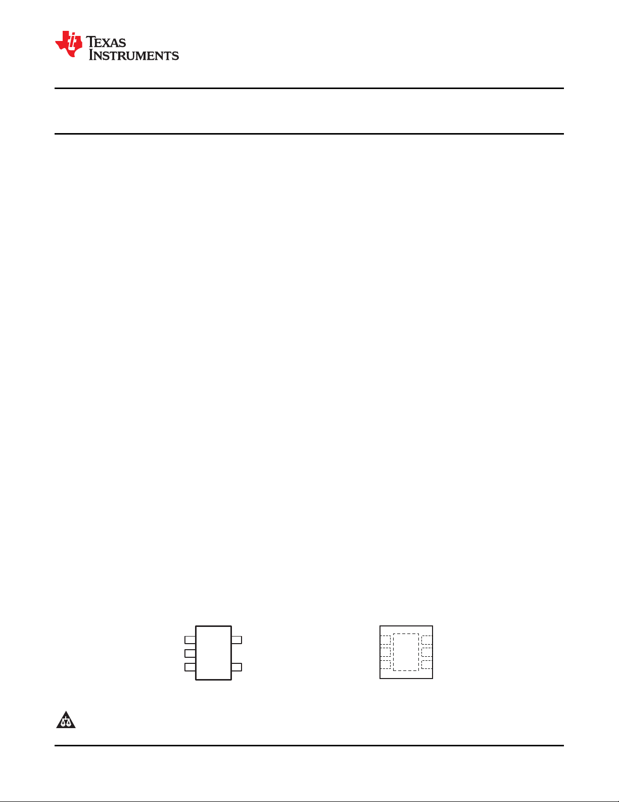
TPS780DDC
TSOT23-5
(TOPVIEW)
OUT
V /FB
SET
IN
GND
EN
1
2
3
5
4
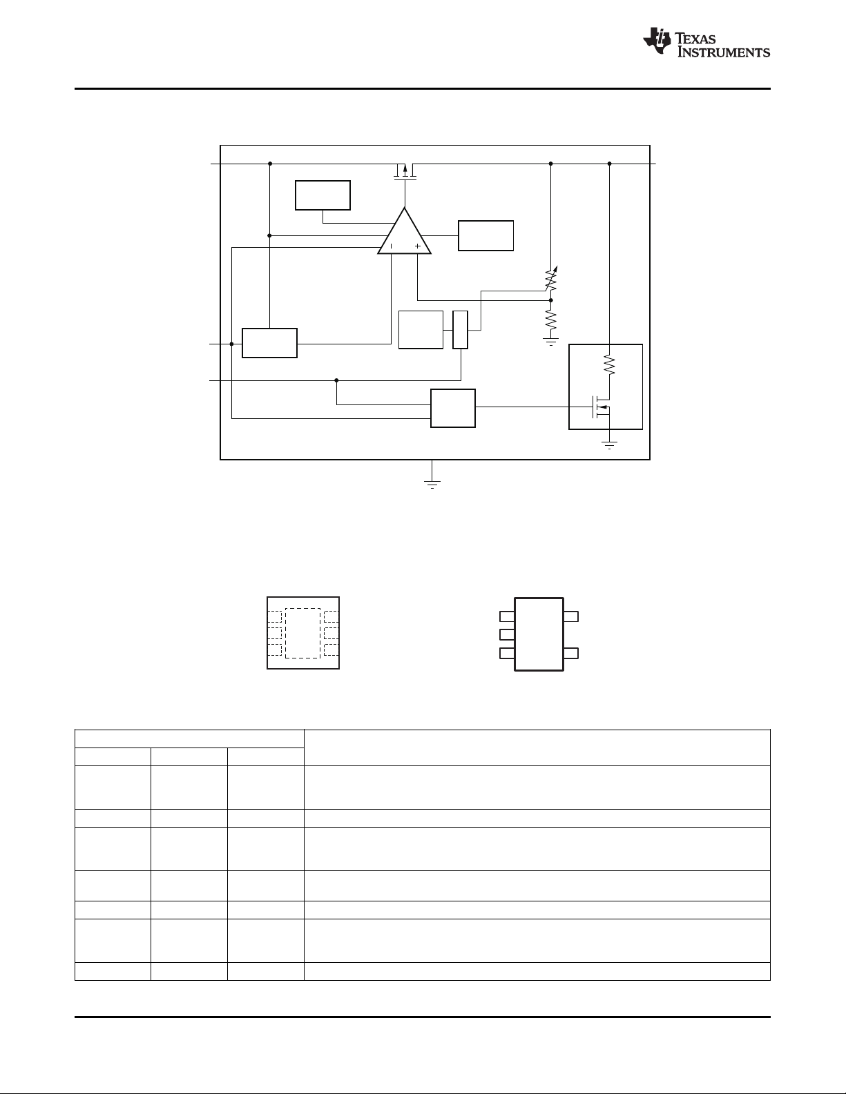
TPS780DRV
2mmx2mmSON-6
(TOPVIEW)
IN
GND
EN
6
5
4
OUT
N/C
V FB/
SET
1
2
3
Thermal
Pad
TPS780 Series
www.ti.com
....................................................................................................................................................... SBVS083C – JANUARY 2007 – REVISED MAY 2008
150mA, Low-Dropout Regulator, Ultralow-Power, IQ500nA
with Pin-Selectable, Dual-Level Output Voltage
1
FEATURES
2
• Low IQ: 500nA
• 150mA, Low-Dropout Regulator with
Pin-Selectable Dual Voltage Level Output
• Low Dropout: 200mV at 150mA
• 3% Accuracy Over Load/Line/Temperature
• Available in Dual-Level, Fixed Output Voltages
from 1.5V to 4.2V Using Innovative Factory
EPROM Programming
• Available in an Adjustable Version from 1.22V
to 5.25V or a Dual-Level Output Version
• V
Pin Toggles Output Voltage Between Two
SET
Factory-Programmed Voltage Levels
• Stable with a 1.0 µ F Ceramic Capacitor
• Thermal Shutdown and Overcurrent Protection
• CMOS Logic Level-Compatible Enable Pin
• Available in DDC (TSOT23-5) or DRV (2mm ×
2mm SON-6) Package Options
The V
two voltage levels on-the-fly through a
microprocessor-compatible input. This LDO is
designed specifically for battery-powered applications
where dual-level voltages are needed. With ultralow
IQ(500nA), microprocessors, memory cards, and
smoke detectors are ideal applications for this device.
The ultralow-power and selectable dual-level output
voltages allow designers to customize power
consumption for specific applications. Designers can
now shift to a lower voltage level in a battery-powered
design when the microprocessor is in sleep mode,
further reducing overall system power consumption.
The two voltage levels are preset at the factory
through a unique architecture using an EPROM. The
EPROM technique allows for numerous output
voltage options between V
V
SET
only. Consult with your local factory representative for
exact voltage options and ordering information;
minimum order quantities may apply.
The TPS780 series are designed to be compatible
APPLICATIONS
• TI MSP430 Attach Applications
• Power Rails with Programming Mode
• Dual Voltage Levels for Power-Saving Mode
with the TI MSP430 and other similar products. The
enable pin is compatible with standard CMOS logic.
This LDO is stable with any output capacitor greater
than 1.0 µ F. Therefore, implementations of this device
require minimal board space because of miniaturized
• Wireless Handsets, Smartphones, PDAs, MP3 packaging and a potentially small output capacitor.
Players, and Other Battery-Operated Handheld The TPS780 series IQ(500nA) also come with
Products thermal shutdown and current limit to protect the
device during fault conditions. All packages have an
DESCRIPTION
operating temperature range of T
+125 ° C. For more cost-sensitive applications
The TPS780 family of low-dropout (LDO) regulators
offer the benefits of ultralow power (I
miniaturized packaging (2 × 2 SON-6), and selectable
= 500nA),
Q
requiring a dual-level voltage option and only on par
IQ, consider the TPS781 series , with an IQof 1.0 µ A
and dynamic voltage scaling.
dual-level output voltage levels. An adjustable version
is also available, but does not have the capability to
shift voltage levels.
pin allows the end user to switch between
SET
low (1.5V to 4.2V) and
SET
high (2.0V to 3.0V) in the fixed output version
J
= – 40 ° C to
1
2 All trademarks are the property of their respective owners.
PRODUCTION DATA information is current as of publication date.
Products conform to specifications per the terms of the Texas
Instruments standard warranty. Production processing does not
necessarily include testing of all parameters.
Please be aware that an important notice concerning availability, standard warranty, and use in critical applications of
Texas Instruments semiconductor products and disclaimers thereto appears at the end of this data sheet.
Copyright © 2007 – 2008, Texas Instruments Incorporated
Page 2
TPS780 Series
SBVS083C – JANUARY 2007 – REVISED MAY 2008 .......................................................................................................................................................
www.ti.com
This integrated circuit can be damaged by ESD. Texas Instruments recommends that all integrated circuits be handled with
appropriate precautions. Failure to observe proper handling and installation procedures can cause damage.
ESD damage can range from subtle performance degradation to complete device failure. Precision integrated circuits may be more
susceptible to damage because very small parametric changes could cause the device not to meet its published specifications.
ORDERING INFORMATION
PRODUCT V
TPS780 vvvxxxyyyz VVV is the nominal output voltage for V
XXX is the nominal output voltage for V
YYY is the package designator.
Z is the tape and reel quantity (R = 3000, T = 250).
Adjustable version
(3) (4)
(1) (2)
OUT
OUT(HIGH)
OUT(LOW)
and corresponds to V
and corresponds to V
pin low.
SET
pin high.
SET
(1) For the most current package and ordering information see the Package Option Addendum at the end of this document, or see the TI
web site at www.ti.com .
(2) Additional output voltage combinations are available on a quick-turn basis using innovative, factory EPROM programming.
Minimum-order quantities apply; contact your sales representative for details and availability.
(3) To order the adjustable version, use TPS78001YYYZ.
(4) The device is either fixed voltage, dual-level V
output simultaneously.
ABSOLUTE MAXIMUM RATINGS
, or adjustable voltage only. Device design does not permit a fixed and adjustable
OUT
(1)
At TJ= – 40 ° C to +125 ° C, unless otherwise noted. All voltages are with respect to GND.
PARAMETER TPS780 Series UNIT
Input voltage range, V
Enable and V
SET
Output voltage range, V
Maximum output current, I
IN
voltage range, V
OUT
OUT
and V
EN
VSET
Output short-circuit duration Indefinite
Total continuous power dissipation, P
ESD rating
Human body model (HBM) 2 kV
Charged device model (CDM) 500 V
Operating junction temperature range, T
Storage temperature range, T
DISS
J
STG
(1) Stresses above these ratings may cause permanent damage. Exposure to absolute maximum conditions for extended periods may
degrade device reliability. These are stress ratings only, and functional operation of the device at these or any other conditions beyond
those specified is not implied.
(2) V
and V
EN
absolute maximum rating are VIN+ 0.3V or +6.0V, whichever is less.
VSET
– 0.3 to +6.0 V
– 0.3 to VIN+ 0.3
(2)
– 0.3 to VIN+ 0.3V V
Internally limited
See the Dissipation Ratings table
– 40 to +125 ° C
– 55 to +150 ° C
V
DISSIPATION RATINGS
BOARD PACKAGE R
(1)
High-K
(1)
High-K
DRV 20 ° C/W 65 ° C/W 15.4mW/ ° C 1540mW 845mW 615mW
DDC 90 ° C/W 200 ° C/W 5.0mW/ ° C 500mW 275mW 200mW
θ JC
R
θ JA
(1) The JEDEC high-K (2s2p) board used to derive this data was a 3-inch × 3-inch, multilayer board with 1-ounce internal power and ground
planes and 2-ounce copper traces on top and bottom of the board.
2 Submit Documentation Feedback Copyright © 2007 – 2008, Texas Instruments Incorporated
DERATING FACTOR
ABOVE TA= +25 ° C TA< +25 ° C TA= +70 ° C TA= +85 ° C
Page 3
TPS780 Series
www.ti.com
....................................................................................................................................................... SBVS083C – JANUARY 2007 – REVISED MAY 2008
ELECTRICAL CHARACTERISTICS
Over operating temperature range (T
100 µ A, V
V
V
OUT
V
V
OUT_RANGE
Δ V
OUT
Δ V
OUT
V
V
V
V
I
CL
I
GND
I
SHDN
I
VSET
I
EN
I
FB
PSRR Power-supply rejection ratio V
t
TR(H → L)
t
TR(L → H)
t
STR
t
SHDN
T
T
(1) The output voltage for V
(2) Adjustable version only.
(3) No V
(4) No dynamic voltage scaling on the adjustable version.
(5) V
DO
(6) I
GND
(7) The TPS78001 FB pin is tied to V
(8) Time from V
(9) Time from V
(10) See Shutdown in the Application Information section for more details.
= V
VSET
= VIN, C
EN
OUT
PARAMETER TEST CONDITIONS MIN TYP MAX UNIT
IN
FB
Input voltage range 2.2 5.5 V
(1)
DC output accuracy
Internal reference
(adjustable version only)
Output voltage range
(adjustable version only)
/ Δ V
Line regulation V
IN
/ Δ I
DO
N
HI
LO
Load regulation 0mA ≤ I
OUT
Dropout voltage
(5)
Output noise voltage 86 µ V
V
high (output V
SET
selected), or EN high (enabled)
V
low (output V
SET
selected), or EN low (disabled)
Output current limit V
Ground pin current
Shutdown current (I
V
pin current V
SET
EN pin current V
FB pin current
(7)
(adjustable version only)
V
transition time (high-to-low) V
OUT
V
= 97% × V
SD
J
SET
OUT
V
transition time (low-to-high) V
OUT
V
= 97% × V
OUT
Startup time
Shutdown time
Thermal shutdown temperature
Operating junction temperature – 40 +125 ° C
pin on the adjustable version.
OUT(HIGH)
OUT(LOW)
(8)
(9)
= low/high is programmed at the factory.
SET
is not measured for devices with V
= 800nA (max) up to +100 ° C.
= 1.2V to V
EN
EN
= 0.4V to V
OUT
OUT
(2)
= – 40 ° C to +125 ° C), V
J
= 1.0 µ F, fixed or adjustable, unless otherwise noted. Typical values at TJ= +25 ° C.
Nominal TJ= +25 ° C, V
Over VIN, I
temperature 0mA ≤ I
(3) (4)
OUT(LOW)
OUT(HIGH)
) 18 130 nA
GND
OUT(NOM)
. Adjustable version only.
OUT
= 90% (V
= 10% (V
, V
OUT
OUT
TJ= +25 ° C, VIN= 4.0V, I
VIN= 5.5V, I
OUT(NOM)
VIN= 95% V
BW = 100Hz to 100kHz, VIN= 2.2V,
V
OUT
OUT
I
OUT
I
OUT
V
EN
TJ= – 40 ° C to +100 ° C
EN
EN
VIN= 5.5V, V
VIN= 4.3V,
OUT
I
OUT
OUT_LOW
I
OUT
OUT_HIGH
I
OUT
C
OUT
V
OUT
I
OUT
V
OUT
V
OUT(NOM)
Shutdown, temperature increasing +160 ° C
Reset, temperature decreasing +140 ° C
< 2.3V because minimum VIN= 2.2V.
OUT(NOM)
OUT(NOM)
).
).
= V
IN
OUT(NOM)
+ 0.5V or 2.2V, whichever is greater; I
=
OUT
TPS780 Series
= high/low – 2 ± 1 +2 %
SET
+ 0.5V ≤ VIN≤ 5.5V,
≤ 150mA, V
OUT
= 100 µ A
OUT
+ 0.5V ≤ VIN≤ 5.5V, I
≤ 150mA – 2 +2 %
OUT
OUT(NOM)
= 1.2V, I
= 1mA
OUT
= high/low
SET
= 75mA 1.216 V
OUT
(2)
= 5mA – 1 +1 %
OUT
, I
= 150mA 250 mV
OUT
– 3.0 ± 2.0 +3.0 %
V
1.2 V
5.25 V
FB
IN
0 0.4 V
= 0.90 × V
= 0mA
OUT(NOM)
(6)
150 230 400 mA
420 800 nA
= 150mA 5 µ A
≤ 0.4V, 2.2V ≤ VIN< 5.5V,
= V
= V
= 5.5V 70 nA
VSET
= 5.5V 40 nA
VSET
OUT
= 1.2V, I
= 100 µ A 10 nA
OUT
f = 10Hz 40 dB
= 3.3V, f = 100Hz 20 dB
= 150mA
= 2.2V, V
= 10mA
= 3.3V, V
= 10mA
= 1.0 µ F, V
= 90% V
= 150mA, C
= 90% V
OUT(NOM)
OUT(NOM)
f = 1kHz 15 dB
= 1.0 µ F, V
to V
= 3.3V,
= 2.2V,
OUT(NOM)
OUT
to
= 2.8V,
OUT
= 10% 500
800 µ s
800 µ s
500 µ s
(10)
OUT(HIGH)
OUT(LOW)
= 10% V
OUT
OUT
RMS
V
µ s
Copyright © 2007 – 2008, Texas Instruments Incorporated Submit Documentation Feedback 3
Page 4
Thermal
Shutdown
10kW
Current
Limit
Bandgap
IN
EN
OUT
EPROM
MUX
V
SET
/FB
(1)
LOGIC
Active
Pull-
Down
GND
TPS780DRV
2mmx2mmSON-6
(TOPVIEW)
IN
GND
EN
6
5
4
OUT
N/C
V FB/
SET
1
2
3
Thermal
Pad
(1)
TPS780DDC
TSOT23-5
(TOPVIEW)
OUT
V /FB
SET
IN
GND
EN
1
2
3
5
4
TPS780 Series
SBVS083C – JANUARY 2007 – REVISED MAY 2008 .......................................................................................................................................................
www.ti.com
FUNCTIONAL BLOCK DIAGRAM
(1) Feedback pin (FB) for adjustable versions; V
SET
for fixed voltage versions.
PIN CONFIGURATIONS
(1) It is recommended that the SON package thermal pad be connected to ground.
Table 1. TERMINAL FUNCTIONS
TERMINAL
NAME DRV DDC DESCRIPTION
Regulated output voltage pin. A small (1 µ F) ceramic capacitor is needed from this pin to
OUT 1 5 ground to assure stability. See the Input and Output Capacitor Requirements in the
Application Information section for more details.
N/C 2 — Not connected.
Feedback pin (FB) for adjustable versions; V
V
/FB 3 4 pin (V
SET
EN 4 3
selects preset output voltage low.
) below 0.4V selects preset output voltage high. Driving the V
SET
Driving the enable pin (EN) over 1.2V turns on the regulator. Driving this pin below 0.4V puts
the regulator into shutdown mode, reducing operating current to 18nA typical.
GND 5 2 Ground pin.
IN 6 1 capacitor = 1.0 µ F. Both input and output capacitor grounds should be tied back to the IC
Thermal pad Thermal pad — It is recommended that the SON package thermal pad be connected to ground.
4 Submit Documentation Feedback Copyright © 2007 – 2008, Texas Instruments Incorporated
Input pin. A small capacitor is needed from this pin to ground to assure stability. Typical input
ground with no significant impedance between them.
for fixed voltage versions. Driving the select
SET
pin over 1.2V
SET
Page 5
2.2 2.7 3.2 3.7 4.2 4.7 5.2 5.7
V (V)
IN
V (%)
OU
T
0.3
0.2
0.1
0
-0.1
-0.2
-0.3
TJ=+85°C
TJ=+25°C
T = 40- °JC
TJ=+125°C
2.7 3.2 3.7 4.2 4.7 5.2 5.7
V (V)
IN
V (%)
O
UT
1.0
0.8
0.6
0.4
0.2
0
-0.2
-0.4
-0.6
-0.8
-1.0
TJ=+125°C
T = 40- °JC
TJ=+25°C
TJ=+85°C
2.7 3.2 3.7 4.2 4.7 5.2 5.7
V (V)
IN
V (%)
OUT
3
2
1
0
-1
-2
-3
TJ=+85°C
T = 40- °JC
TJ=+25°C
3.8 4.0 4.2 4.4 4.6 4.8 5.0 5.2 5.4 5.6
V (V)
IN
V (%)
OUT
1.0
0.8
0.6
0.4
0.2
0
-0.2
-0.4
-0.6
-0.8
-1.0
T =+85°JC
T = 40- °JC
T =+25°JC
3.8 4.0 4.2 4.4 4.6 4.8 5.0 5.2 5.4 5.6
V (V)
IN
V (%)
OU
T
3
2
1
0
-1
-2
-3
TJ=+85°C
T 40- °
J
= C
TJ=+25°C
0 25 50 75 100 125 150
I (mA)
OUT
V (%)
O
UT
1.5
1.0
0.5
0
-0.5
-1.0
TJ=+125°C
TJ=+25°C
T = 40- °JC
TJ=+85°C
TPS780 Series
www.ti.com
....................................................................................................................................................... SBVS083C – JANUARY 2007 – REVISED MAY 2008
TYPICAL CHARACTERISTICS
Over the operating temperature range of TJ= – 40 ° C to +125 ° C, V
I
I
OUT
OUT
I
OUT
= 150mA, V
= 100 µ A, V
LINE REGULATION LINE REGULATION
= 5mA, V
TPS78001 TPS780330220
Figure 1. Figure 2.
LINE REGULATION LINE REGULATION
VSET
TPS780330220 TPS780330220
= V
EN
= 1.22V (typ) I
OUT
= 1.2V, V
= VIN, C
VSET
= 2.2V (typ) I
OUT
OUT
= 1 µ F, and C
= V
IN
OUT(TYP)
= 1 µ F, unless otherwise noted.
IN
= 5mA, V
OUT
= 5mA, V
OUT
+ 0.5V or 2.2V, whichever is greater;
= 1.2V, V
VSET
= 0.4V, V
VSET
OUT
OUT
= 2.2V (typ)
= 3.3V (typ)
Figure 3. Figure 4.
LINE REGULATION LOAD REGULATION
I
= 150mA, V
OUT
Copyright © 2007 – 2008, Texas Instruments Incorporated Submit Documentation Feedback 5
VSET
TPS780330220 TPS78001
Figure 5. Figure 6.
= 0.4V, V
= 3.3V (typ) V
OUT
= 3.3V
OUT
Page 6
0 25 50 75 100 125 150
I (mA)
OUT
V (%)
OUT
3.0
2.5
2.0
1.5
1.0
0.5
0
-0.5
-1.0
-1.5
-2.0
TJ=+85°C
T = 40- °JC
TJ=+25°C
0 25 50 75 100 125 150
I (mA)
OUT
V (%)
OUT
3
2
1
0
-1
-2
-3
TJ=+85°C
T = 40- °JC
TJ=+25°C
0 25 50 75 100 125 150
I (mA)
OUT
V (V V-
DO IN
OUT
)(mV)
200
180
160
140
120
100
80
60
40
20
0
TJ=+85°C
T = 40- °JC
TJ=+125°C
TJ=+25°C
0 25 50 75 100 125 150
I (mA)
OUT
V (V V-
DO IN OUT
)(mV)
250
200
150
100
50
0
TJ=+125°C
TJ=+85°C
T = 40- °JC
TJ=+25°C
-40 -25 -10 1251109580655035205
Temperature( C)°
V (V V-
DO IN OUT
)(mV)
250
200
150
100
50
0
150mA
100mA
50mA
10mA
-40 -25 -10 1251109580655035205
Temperature( C)°
V (V V-
DO IN OUT
)(mV)
250
200
150
100
50
0
150mA
100mA
50mA
10mA
TPS780 Series
SBVS083C – JANUARY 2007 – REVISED MAY 2008 .......................................................................................................................................................
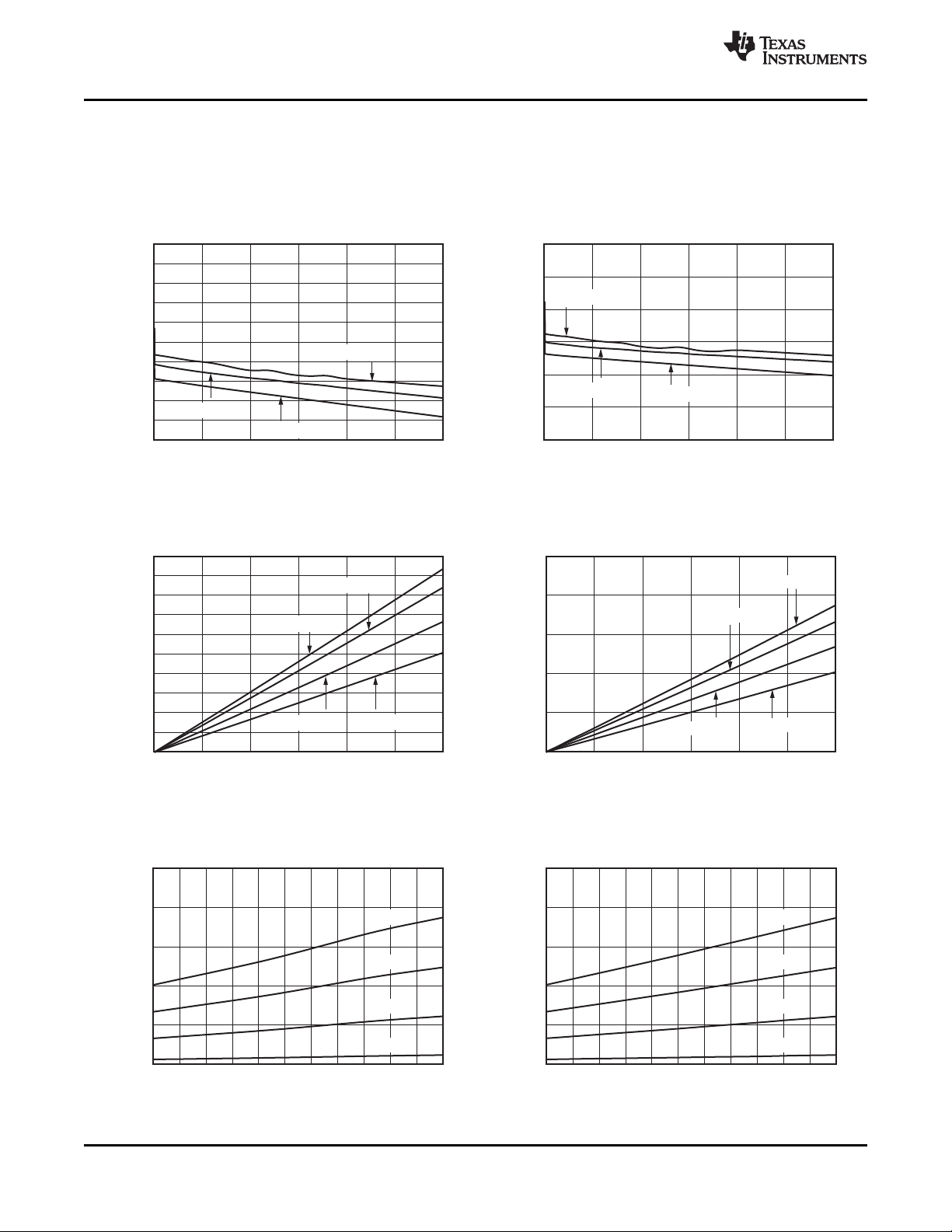
TYPICAL CHARACTERISTICS (continued)
Over the operating temperature range of TJ= – 40 ° C to +125 ° C, V
I
OUT
= 100 µ A, V
= V
EN
= VIN, C
VSET
= 1 µ F, and C
OUT
= 1 µ F, unless otherwise noted.
IN
LOAD REGULATION LOAD REGULATION
V
= 1.2V, VIN= 2.7V, V
VSET
TPS780330220 TPS780330220
= 2.2V V
OUT
Figure 7. Figure 8.
DROPOUT VOLTAGE vs OUTPUT CURRENT DROPOUT VOLTAGE vs OUTPUT CURRENT
V
= 3.3V (typ), VIN= 0.95 × V
OUT
TPS78001 TPS780330220
(typ) V
OUT
www.ti.com
= V
IN
OUT(TYP)
+ 0.5V or 2.2V, whichever is greater;
= 0.4V, VIN= 3.8V, V
VSET
= 0.4V, V
VSET
OUT
= 3.3V
OUT
= 3.3V (typ), VIN= 0.95 × V
(typ)
OUT
DROPOUT VOLTAGE vs TEMPERATURE DROPOUT VOLTAGE vs TEMPERATURE
V
= 3.3V (typ), VIN= 0.95 × V
OUT
6 Submit Documentation Feedback Copyright © 2007 – 2008, Texas Instruments Incorporated
Figure 9. Figure 10.
(typ) V
TPS78001 TPS780330220
OUT
= 0.4V, V
VSET
= 3.3V (typ), VIN= 0.95 × V
OUT
Figure 11. Figure 12.
(typ)
OUT
Page 7
2.2 2.7 3.2 3.7 4.2 4.7 5.2 5.7
V (V)
IN
I A)m
GND
(
6
5
4
3
2
1
0
T C°
J
=+125
T C°
J
=+85
T = 40- °JC
T C°
J
=+25
2.2 2.7 3.2 3.7 4.2 4.7 5.2 5.7
V (V)
IN
I
(
A)m
GND
8
7
6
5
4
3
2
1
0
T =+125 C°
J
T =+85 C°
J
TJ= 40- °C
T =+25 C°
J
2.7 3.2 3.7 4.2 4.7 5.2 5.7
V (V)
IN
I (nA)
GN
D
1000
900
800
700
600
500
400
300
200
100
0
TJ=+125°C
TJ=+85°C
TJ= 40- °C
TJ=+25°C
2.7 3.2 3.7 4.2 4.7 5.2 5.7
V (V)
IN
I (nA)
GN
D
1000
900
800
700
600
500
400
300
200
100
0
T =+125 C°
J
T =+85 C°
J
T = 40- °JC
T =+25 C°
J
2.7 3.2 3.7 4.2 4.7 5.2 5.7
V (V)
IN
I ( A)m
GND
6
5
4
3
2
1
0
T =+125 C°
J
T =+85 C°
J
T 40- °
J
= C
T =+25 C°
J
2.7 3.2 3.7 4.2 4.7 5.2 5.7
V (V)
IN
I ( A)m
GN
D
12
11
10
9
8
7
6
5
4
3
2
1
0
T =+125 CJ°
T =+85 CJ°
T = 40- °JC
T =+25 CJ°
TPS780 Series
www.ti.com
....................................................................................................................................................... SBVS083C – JANUARY 2007 – REVISED MAY 2008
TYPICAL CHARACTERISTICS (continued)
Over the operating temperature range of TJ= – 40 ° C to +125 ° C, V
I
OUT
= 100 µ A, V
= V
EN
= VIN, C
VSET
= 1 µ F, and C
OUT
= 1 µ F, unless otherwise noted.
IN
GROUND PIN CURRENT vs INPUT VOLTAGE GROUND PIN CURRENT vs INPUT VOLTAGE
I
= 50mA, V
OUT
TPS78001 TPS78001
= 1.22V I
OUT
Figure 13. Figure 14.
GROUND PIN CURRENT vs INPUT VOLTAGE GROUND PIN CURRENT vs INPUT VOLTAGE
I
OUT
= 0mA, V
= 1.2V, V
VSET
TPS780330220 TPS780330220
= 2.2V I
OUT
= V
IN
OUT(TYP)
+ 0.5V or 2.2V, whichever is greater;
= 150mA, V
OUT
OUT
= 1mA, V
= 1.2V, V
VSET
= 1.22V
OUT
= 2.2V
OUT
Figure 15. Figure 16.
GROUND PIN CURRENT vs INPUT VOLTAGE GROUND PIN CURRENT vs INPUT VOLTAGE
I
= 50mA, V
OUT
Copyright © 2007 – 2008, Texas Instruments Incorporated Submit Documentation Feedback 7
VSET
TPS780330220 TPS780330220
Figure 17. Figure 18.
= 1.2V, V
= 2.2V I
OUT
OUT
= 150mA, V
= 1.2V, V
VSET
= 2.2V
OUT
Page 8
3.8 4.0 4.2 4.4 4.6 4.8 5.0 5.2 5.4 5.6
V (V)
IN
I
(nA)
GND
1000
900
800
700
600
500
400
300
200
100
0
T =+125 C°
J
T =+85 C°
J
TJ= 40- °C
T =+25 C°
J
3.8 4.0 4.2 4.4 4.6 4.8 5.0 5.2 5.4 5.6
V (V)
IN
I
(nA)
GND
1000
900
800
700
600
500
400
300
200
100
0
T °
J
=+125 C
T °
J
=+85 C
TJ= 40- °C
T °
J
=+25 C
3.8 4.0 4.2 4.4 4.6 4.8 5.0 5.2 5.4 5.6
V (V)
IN
I
(
A)m
GND
6
5
4
3
2
1
0
T =+125 C°
J
T =+85 C°
J
T 40- °
J
= C
T =+25 C°
J
3.8 4.0 4.2 4.4 4.6 4.8 5.0 5.2 5.4 5.6
V (V)
IN
I
( A)m
GND
9
8
7
6
5
4
3
2
1
0
T =+125 C°
J
T =+85 C°
J
TJ= -40°C
T =+25 C°
J
0 25 50 75 100 125 150
I (mA)
OUT
I ( A)m
GND
10
8
6
4
2
0
T =+125 C°
J
T =+85 C°
J
T = 40- °JC
T =+25 C°
J
0 25 50 75 100 125 150
I (mA)
OUT
I ( A)m
GND
10
8
6
4
2
0
T =+125 C°
J
T =+85 C°
J
TJ= 40- °C
T =+25 C°
J
TPS780 Series
SBVS083C – JANUARY 2007 – REVISED MAY 2008 .......................................................................................................................................................
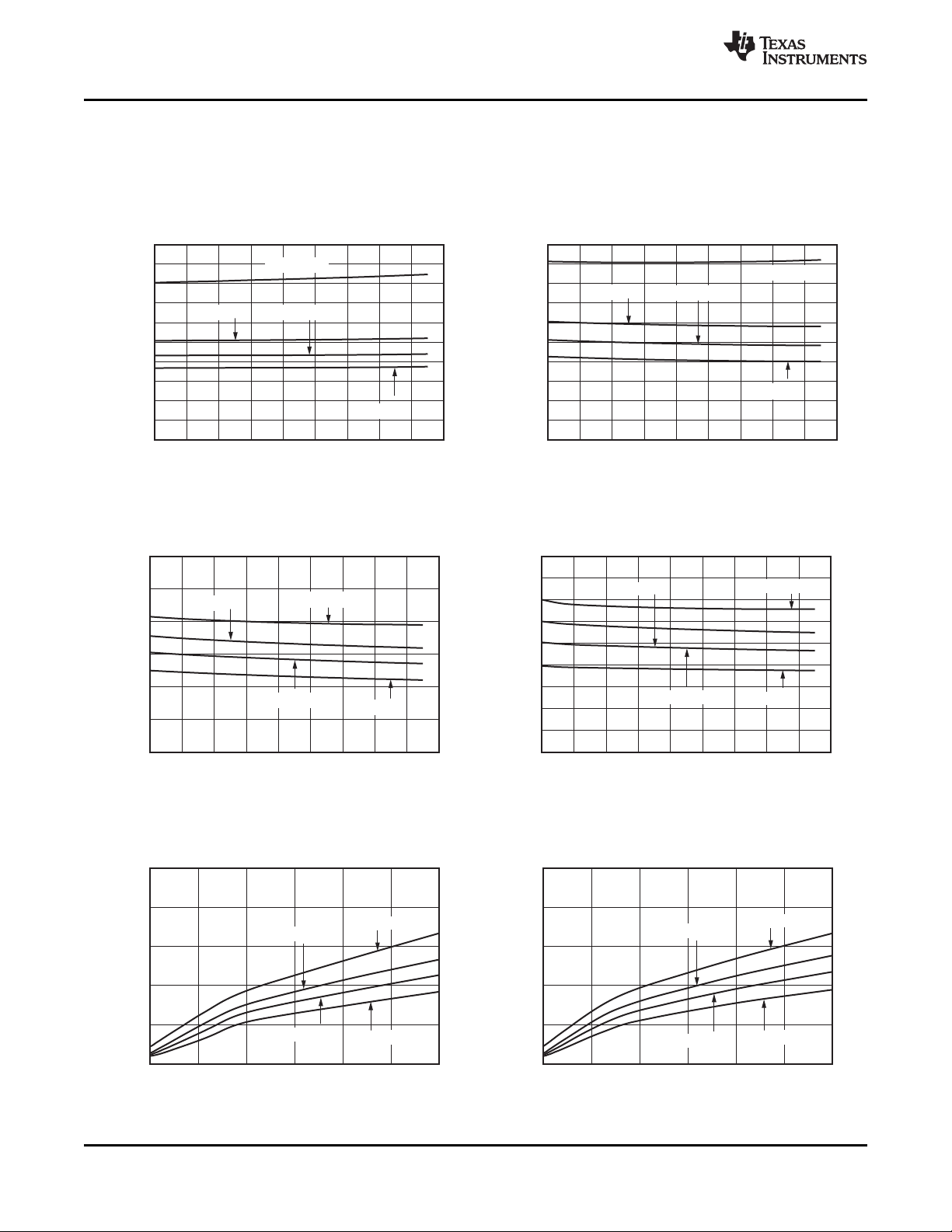
TYPICAL CHARACTERISTICS (continued)
Over the operating temperature range of TJ= – 40 ° C to +125 ° C, V
I
OUT
= 100 µ A, V
= V
EN
= VIN, C
VSET
= 1 µ F, and C
OUT
= 1 µ F, unless otherwise noted.
IN
GROUND PIN CURRENT vs INPUT VOLTAGE GROUND PIN CURRENT vs INPUT VOLTAGE
I
OUT
= 0mA, V
= 0.4V, V
VSET
TPS780330220 TPS780330220
= 3.3V I
OUT
Figure 19. Figure 20.
GROUND PIN CURRENT vs INPUT VOLTAGE GROUND PIN CURRENT vs INPUT VOLTAGE
I
OUT
= 50mA, V
= 0.4V, V
VSET
TPS780330220 TPS780330220
= 3.3V I
OUT
www.ti.com
= V
IN
OUT(TYP)
+ 0.5V or 2.2V, whichever is greater;
OUT
OUT
= 1mA, V
= 150mA, V
= 0.4V, V
VSET
= 0.4V, V
VSET
= 3.3V
OUT
= 3.3V
OUT
Figure 21. Figure 22.
GROUND PIN CURRENT vs OUTPUT CURRENT GROUND PIN CURRENT vs OUTPUT CURRENT
V
= 1.2V, VIN= 5.5V, V
VSET
8 Submit Documentation Feedback Copyright © 2007 – 2008, Texas Instruments Incorporated
TPS780330220 TPS780330220
Figure 23. Figure 24.
= 2.2V V
OUT
= 0.4V, VIN= 5.5V, V
VSET
= 3.3V
OUT
Page 9

2.2 2.7 3.2 3.7 4.2 4.7 5.2 5.7
V (V)
IN
I
(nA)
GND
60
50
40
30
20
10
0
TJ=+85°C
T = 40- °JC
TJ=+25°C
2.2 2.7 3.2 3.7 4.2 4.7 5.2 5.7
V (V)
IN
CurrentLimit(mA)
280
270
260
250
240
230
220
210
200
T =+85 C°
J
T = 40- °JC
T =+25 C°
J
2.7 3.2 3.7 4.2 4.7 5.2 5.7
V (V)
IN
CurrentLimit(mA)
300
290
280
270
260
250
240
230
220
210
200
T =+125 C°
J
T =+85 C°
J
T = 40- °JC
T =+25 C°
J
3.8 4.0 4.2 4.4 4.6 4.8 5.0 5.2 5.4 5.6
V (V)
IN
CurrentLimit(mA)
300
290
280
270
260
250
240
230
220
210
200
TJ=+125°C
TJ=+85°C
T = 40- °JC
TJ=+25°C
-40 -25 -10 1251109580655035205
Temperature( C)°
I
(nA)
FB
5
4
3
2
1
0
V min
IN
V max
IN
2.7 3.2 3.7 4.2 4.7 5.2 5.7
V (V)
IN
I (nA)
VSET
1.0
0.8
0.6
0.4
0.2
0
TJ=+85°C
T = 40- °JC
TJ=+25°C
TPS780 Series
www.ti.com
....................................................................................................................................................... SBVS083C – JANUARY 2007 – REVISED MAY 2008
TYPICAL CHARACTERISTICS (continued)
Over the operating temperature range of TJ= – 40 ° C to +125 ° C, V
I
OUT
= 100 µ A, V
V
VSET
= V
EN
= VIN, C
VSET
= 1 µ F, and C
OUT
= 1 µ F, unless otherwise noted.
IN
SHUTDOWN CURRENT vs INPUT VOLTAGE CURRENT LIMIT vs INPUT VOLTAGE
I
= 0mA, V
OUT
TPS78001 TPS78001
= 0.4V V
VSET
Figure 25. Figure 26.
CURRENT LIMIT vs INPUT VOLTAGE CURRENT LIMIT vs INPUT VOLTAGE
= 1.2V, V
= 95% V
OUT
TPS780330220 TPS780330220
(typ), V
OUT
= 2.2V (typ) V
OUT
= V
IN
OUT(TYP)
+ 0.5V or 2.2V, whichever is greater;
= 90% V
OUT
= 0.4V, V
VSET
OUT
OUT
= 95% V
(typ), V
= 1.22V (typ)
OUT
(typ), V
OUT
= 3.3V (typ)
OUT
Figure 27. Figure 28.
FEEDBACK PIN CURRENT vs TEMPERATURE V
I
= 0mA, V
OUT
TPS78001 TPS780330220
Copyright © 2007 – 2008, Texas Instruments Incorporated Submit Documentation Feedback 9
Figure 29. Figure 30.
= 1.22V I
OUT
PIN CURRENT vs INPUT VOLTAGE
SET
= 100 µ A, V
OUT
= 1.2V, V
VSET
= 2.2V
OUT
Page 10

3.8 4.0 4.2 4.4 4.6 4.8 5.0 5.2 5.4 5.6
V (V)
IN
I
(nA)
VSET
2.5
2.0
1.5
1.0
0.5
0
-0.5
TJ=+125°C
TJ=+85°C
T = 40- °JC
TJ=+25°C
2.2 2.7 3.2 3.7 4.2 4.7 5.2 5.7
V (V)
IN
I (nA)
EN
2.0
1.8
1.6
1.4
1.2
1.0
0.8
0.6
0.4
0.2
0
T =+85 C°
J
T 40°
J
= - C
T =+25 C°
J
2.7 3.2 3.7 4.2 4.7 5.2 5.7
V (V)
IN
I (nA)
EN
2.0
1.8
1.6
1.4
1.2
1.0
0.8
0.6
0.4
0.2
0
T =+85 C°
J
TJ= 40- °C
T =+25 C°
J
3.8 4.0 4.2 4.4 4.6 4.8 5.0 5.2 5.4 5.6
V (V)
IN
I (nA)
EN
2.0
1.8
1.6
1.4
1.2
1.0
0.8
0.6
0.4
0.2
0
TJ=+85°C
T = 40- °JC
TJ=+25°C
-40 -25 -10 1251109580655035205
Temperature( C)°
V (V)
EN
1.2
1.1
1.0
0.9
0.8
0.7
0.6
0.5
0.4
V On
EN
V Off
EN
-40 -25 -10 1251109580655035205
Temperature( C)°
V (V)
EN
1.2
1.1
1.0
0.9
0.8
0.7
0.6
0.5
0.4
V On
EN
V Off
EN
TPS780 Series
SBVS083C – JANUARY 2007 – REVISED MAY 2008 .......................................................................................................................................................
TYPICAL CHARACTERISTICS (continued)
Over the operating temperature range of TJ= – 40 ° C to +125 ° C, V
I
OUT
= 100 µ A, V
= V
EN
V
SET
I
OUT
= VIN, C
VSET
= 1 µ F, and C
OUT
= 1 µ F, unless otherwise noted.
IN
PIN CURRENT vs INPUT VOLTAGE ENABLE PIN CURRENT vs INPUT VOLTAGE
= 100 µ A, V
= 0.4V, V
VSET
TPS780330220 TPS78001
= 3.3V I
OUT
Figure 31. Figure 32.
ENABLE PIN CURRENT vs INPUT VOLTAGE ENABLE PIN CURRENT vs INPUT VOLTAGE
I
OUT
= 100 µ A, V
= 1.2V, V
VSET
TPS780330220 TPS780330220
= 2.2V I
OUT
www.ti.com
= V
IN
OUT(TYP)
+ 0.5V or 2.2V, whichever is greater;
= 1mA, V
OUT
OUT
= 100 µ A, V
OUT
= 0.4V, V
VSET
= 1.22V
= 3.3V
OUT
Figure 33. Figure 34.
ENABLE PIN HYSTERESIS vs TEMPERATURE ENABLE PIN HYSTERESIS vs TEMPERATURE
I
= 1mA, TPS78001 I
OUT
Figure 35. Figure 36.
10 Submit Documentation Feedback Copyright © 2007 – 2008, Texas Instruments Incorporated
= 1mA, TPS780330220
OUT
Page 11

-40 -25 -10 1251109580655035205
Temperature( C)°
%V (V)
O
UT
0.4
0.3
0.2
0.1
0
-0.1
-0.2
-0.3
-0.4
-40 -25 -10 1251109580655035205
Temperature( C)°
%
DV
OUT
(V)
1
0
-1
-2
150mA
0.1mA
5mA
-40 -25 -10 1251109580655035205
Temperature( C)°
%
V
(V)
D
OUT
3
2
1
0
-1
-2
-3
150mA
0.1mA
5mA
10 100 1k 10k 100k
Frequency(Hz)
OutputSpectralNoiseDensity( V/ )m
ÖHz
100
10
1
0.1
0.01
0.001
150mA
109 Vm
RMS
50mA
109 Vm
RMS
1mA
108 Vm
RMS
V
oltage(1V/div)
Time(20ms/div)
LoadCurrent
Enable
V
OUT
V
IN
V =0.0VtoIN5.0V
V =3.3V
OUT
I =150mA
OUT
C =10 Fm
OUT
0V
Current(50mA/div)
10 10M100 1k 10k 100k 1M
Frequency(Hz)
PSRR(dB)
80
70
60
50
40
30
20
10
0
150mA
50mA
1mA
TPS780 Series
www.ti.com
....................................................................................................................................................... SBVS083C – JANUARY 2007 – REVISED MAY 2008
TYPICAL CHARACTERISTICS (continued)
Over the operating temperature range of TJ= – 40 ° C to +125 ° C, V
I
OUT
= 100 µ A, V
= V
EN
VSET
% Δ V
I
= 1mA, VIN= 3.8V, V
OUT
% Δ V
V
= 0.4V, VIN= 3.8V, V
VSET
= VIN, C
vs TEMPERATURE % Δ V
OUT
TPS78001 TPS780330220
= 1 µ F, and C
OUT
= 1 µ F, unless otherwise noted.
IN
= 3.3V V
OUT
Figure 37. Figure 38.
vs TEMPERATURE OUTPUT SPECTRAL NOISE DENSITY vs FREQUENCY
OUT
TPS780330220 TPS780330220
= 3.3V (typ) CIN= 1 µ F, C
OUT
= V
IN
OUT(TYP)
+ 0.5V or 2.2V, whichever is greater;
vs TEMPERATURE
OUT
= 1.2V, VIN= 2.7V, V
VSET
= 2.2 µ F, V
OUT
VSET
= 2.2V (typ)
OUT
= 1.2V, VIN= 2.7V
RIPPLE REJECTION vs FREQUENCY
VIN= 2.7V, V
Copyright © 2007 – 2008, Texas Instruments Incorporated Submit Documentation Feedback 11
Figure 39. Figure 40.
OUT
TPS78001 TPS780330220
Figure 41. Figure 42.
= 1.2V, C
= 2.2 µ F INPUT VOLTAGE RAMP vs OUTPUT VOLTAGE
OUT
Page 12

Voltage(1V/div)
Time(20ms/div)
V =5.5V
IN
V =3.3V
OUT
I =150mA
OUT
C =10 Fm
OUT
V
IN
V
OUT
LoadCurrent
Enable
0V
Current(50mA/div)
Voltage(1V/div)
Time(1ms/div)
LoadCurrent
V =0.0Vto5.5V
IN
V =2.2V
OUT
I =100mA
OUT
C =10 Fm
OUT
V
SET
V
IN
V
OUT
0A
0V
Current(50mA/div)
1V/div
Time(200 s/div)m
V =4.0Vto4.5V
IN
V =2.2V
OUT
I =150mA
OUT
SlewRate=1V/ sm
V
IN
V
OUT
1V/div
Time(200 s/div)m
V =4.0Vto4.5V
IN
V =3.3V
OUT
I =150mA
OUT
SlewRate=1V/ sm
V
IN
V
OUT
Voltage
(100mV/div)
Time(5ms/div)
Load
Current
V =5.5V
IN
V =3.3V
OUT
I =0mAto10mA
OUT
C =10 Fm
OUT
V
OUT
Enable
V
IN
Current
(10mA/div)
0A
Voltage
(100mV/div)
Time(2ms/div)
Load
Current
V =5.5V
IN
V =3.3V
OUT
I =0mAto60mA
OUT
C =10 Fm
OUT
V
IN
V
OUT
Enable
0A
Current
(20mA/div)
TPS780 Series
SBVS083C – JANUARY 2007 – REVISED MAY 2008 .......................................................................................................................................................
TYPICAL CHARACTERISTICS (continued)
Over the operating temperature range of TJ= – 40 ° C to +125 ° C, V
I
OUT
= 100 µ A, V
= V
EN
= VIN, C
VSET
= 1 µ F, and C
OUT
= 1 µ F, unless otherwise noted.
IN
OUTPUT VOLTAGE vs ENABLE (SLOW RAMP) INPUT VOLTAGE vs DELAY TO OUTPUT
TPS780330220 TPS780330220
Figure 43. Figure 44.
LINE TRANSIENT RESPONSE LINE TRANSIENT RESPONSE
TPS780330220 TPS780330220
www.ti.com
= V
IN
OUT(TYP)
+ 0.5V or 2.2V, whichever is greater;
Figure 45. Figure 46.
LOAD TRANSIENT RESPONSE LOAD TRANSIENT RESPONSE
TPS780330220 TPS780330220
12 Submit Documentation Feedback Copyright © 2007 – 2008, Texas Instruments Incorporated
Figure 47. Figure 48.
Page 13

Voltage(1V/div)
Time(1ms/div)
LoadCurrent
V =5.50V
IN
V =3.3V
OUT
I =150mA
OUT
C
OUT
=10mF
V
IN
V
OUT
Enable
0V
Current(50mA/div)
Voltage(1V/div)
Time(1ms/div)
Load
Current
V =5.5V
IN
V =3.3V
OUT
I =150mA
OUT
C =10 Fm
OUT
V
IN
V
OUT
Enable
0V
Current(50mA/div)
1V/div
Time(500ms/div)
VIN=5.0V
Enable=V
IN
I
OUT
=150mA
V Transitioningfrom2.2Vto3.3V
OUT
V
OUT
V
SET
1V/div
Time(500 s/div)m
V =5.0V
IN
I =150mA
OUT
V Transitioningfrom3.3Vto2.2V
OUT
V
OUT
V
SET
Voltage(1V/div)
Time(50ms/div)
V
SET
V =5.5V
IN
V =3.3V
OUT
I =150mA
OUT
to100mA
C =10 Fm
OUT
V
IN
V
OUT
LoadCurrent
0A
50mA
100mA
Current(50mA/div)
TPS780 Series
www.ti.com
....................................................................................................................................................... SBVS083C – JANUARY 2007 – REVISED MAY 2008
TYPICAL CHARACTERISTICS (continued)
Over the operating temperature range of TJ= – 40 ° C to +125 ° C, V
I
OUT
= 100 µ A, V
ENABLE PIN vs OUTPUT VOLTAGE RESPONSE
= V
EN
= VIN, C
VSET
= 1 µ F, and C
OUT
= 1 µ F, unless otherwise noted.
IN
AND OUTPUT CURRENT ENABLE PIN vs OUTPUT VOLTAGE DELAY
TPS780330220 TPS780330220
Figure 49. Figure 50.
V
PIN TOGGLE V
SET
TPS780330220 TPS780330220
= V
IN
OUT(TYP)
+ 0.5V or 2.2V, whichever is greater;
PIN TOGGLE
SET
Copyright © 2007 – 2008, Texas Instruments Incorporated Submit Documentation Feedback 13
Figure 51. Figure 52.
V
PIN TOGGLE (SLOW RAMP)
SET
TPS780330220
Figure 53.
Page 14

V =V 1+´
OUT FB
R
R
1
2
()
R
1 2
= 1 R- ´
V
V
OUT
FB
()
TPS780
GND
EN
V
SET
IN OUT
V
IN
V
OUT
1 Fm
1 Fm
4.2Vto5.5V 2.2Vto3.3V
On
Off
V High=V
SET OUT(LOW)
V Low=V
SET OUT(HIGH)
TPS78001
GND
EN
IN OUT
V
IN
V
OUT
1 Fm
1 Fm
FB
R
1
R
2
V =V (1+)´
OUT FB
R
R
1
2
TPS780 Series
SBVS083C – JANUARY 2007 – REVISED MAY 2008 .......................................................................................................................................................
APPLICATION INFORMATION
APPLICATION EXAMPLES
The TPS780 series of LDOs typically take less than
800 µ s to transition from a lower voltage of 2.2V to a
higher voltage of 3.3V under an output load of
150mA; see Figure 51 . Additionally, the TPS780
series contain active pull-down circuitry that
automatically pulls charge out of the voltage capacitor
to transition the output voltage from the higher
voltage to the lower voltage, even with no load
connected. Output voltage overshoots and
undershoots are minimal under this load condition.
The TPS780 series typically take less than 800 µ s to
transition from V
(2.2V to 3.3V); see Figure 51 and Figure 52 . Both
output states of the TPS780 series are
factory-programmable between 1.5V to 4.2V. Note
that during startup or steady-state conditions, it is
important that the EN pin and V
exceed V
+ 0.3V.
IN
low (3.3V to 2.2V), or V
SET
SET
SET
pin voltages never
www.ti.com
Programming the TPS78001 Adjustable LDO Regulator
The output voltage of the TPS78001 adjustable
regulator is programmed using an external resistor
divider as shown in Figure 55 . The output voltage
operating range is 1.2V to 5.1V, and is calculated
using Equation 1 :
(1)
Where:
V
= 1.216V typ (the internal reference voltage)
high
FB
Resistors R
and R
1
should be chosen for
2
approximately 1.2 µ A divider current. Lower value
resistors can be used for improved noise
performance, but the solution consumes more power.
Higher resistor values should be avoided because
leakage current into/out of FB across R1/R
creates
2
an offset voltage that artificially increases/decreases
the feedback voltage and thus erroneously
decreases/increases V
. Table 2 lists several
OUT
common output voltages and resistor values. The
recommended design procedure is to choose R
=
2
1M Ω to set the divider current at 1.2 µ A, and then
calculate R
using Equation 2 :
1
The TPS780 is also used effectively in dynamic
voltage scaling (DVS) applications. DVS applications
are required to dynamically switch between a high
operational voltage to a low standby voltage in order
to reduce power consumption. Modern multimillion
gate microprocessors fabricated with the latest
sub-micron processes save power by transitioning to
a lower voltage to reduce leakage currents while
maintaining content. This architecture enables the
microprocessor to transition quickly into an
operational state (wake up) without requiring a reload
of the states from external memory, or a reboot.
14 Submit Documentation Feedback Copyright © 2007 – 2008, Texas Instruments Incorporated
Figure 54. Typical Application Circuit
(2)
Figure 55. TPS78001 Adjustable LDO Regulator
Programming
Table 2. Output Voltage Programming Guide
OUTPUT VOLTAGE R
1.8V 0.499M Ω 1M Ω
2.8V 1.33M Ω 1M Ω
5.0V 3.16M Ω 1M Ω
1
R
2
Page 15

LDO
GND
V
IN
V
OUT
1 Fm 1 Fm
MSP430
V
SS
V
CC
I/O
V =3.0V
CC
5mA
Active
Mode
3.0V
1.6 AI
LPM3/SleepMode
m
Q
TPS780
GND
V
IN
V
OUT
MSP430
V
SS
V
CC
I/O
V =3.6V
CC
5mA
Active
Mode
700nAI
LPM3/SleepMode
Q
V =2.2V
CC
Current
1 Fm 1 Fm
2.2Vto3.6V
V
SET
TPS780 Series
www.ti.com
....................................................................................................................................................... SBVS083C – JANUARY 2007 – REVISED MAY 2008
Powering the MSP430 Microcontroller
Several versions of the TPS780 are ideal for
powering the MSP430 microcontroller . Table 3 shows
potential applications of some voltage versions.
Table 3. Typical MSP430 Applications
V
DEVICE (TYP) (TYP) APPLICATION
TPS780360200 3.6V 2.0V
TPS780360220 3.6V 2.2V
TPS780360300 3.6V 3.0V
TPS780360220 3.6V 2.2V MSP430s. Allows
OUT(HIGH)
V
OUT(LOW)
V
OUT, MIN
required by many
MSP430s. Allows
lowest power
consumption
operation.
V
OUT, MIN
required by some
MSP430s FLASH
operation.
V
OUT, MIN
required by some
MSP430s FLASH
operation.
V
OUT, MIN
required by some
highest speed
operation.
> 1.800V
> 2.200V
> 2.700V
< 3.600V
Figure 56. Typical LDO without DVS
The TPS780 family offers many output voltage
versions to allow designers to optimize the supply
voltage for the processing speed required of the
MSP430. This flexible architecture minimizes the
supply current consumed by the particular MSP430
application. The MSP430 total system power can be
reduced by substituting the 500nA IQTPS780 series
LDO in place of an existing ultra-low IQLDO (typical
best case = 1 µ A). Additionally, DVS allows for
increasing the clock speed in active mode (MSP430
V
= 3.6V). The 3.6V V
CC
reduces the MSP430 time
CC
in active mode. In low-power mode, MSP430 system
power can be further reduced by lowering the
MSP430 V
to 2.2V in sleep mode.
CC
Key features of the TPS780 series are an ultralow
quiescent current (500nA), DVS, and miniaturized
packaging. The TPS780 family are available in
SON-6 and TSOT-23 packages. Figure 56 shows a
Figure 57. TPS780 with Integrated DVS
typical MSP430 circuit powered by an LDO without
DVS. Figure 57 is an MSP430 circuit using a TPS780
LDO that incorporates an integrated DVS, thus
simplifying the circuit design. In a circuit without DVS,
as Figure 56 illustrates, V
the MSP430 goes into sleep mode, V
3.0V; if DVS is applied, V
is always at 3.0V. When
CC
CC
remains at
CC
could be reduced in
The other benefit of DVS is that it allows a higher V
voltage on the MSP430, increasing the clock speed
and reducing the active mode dwell time.
sleep mode. In Figure 57 , the TPS780 LDO with
integrated DVS maintains 3.6V V
signal from the MSP430 forces V
V
from 3.6V down to 2.2V, thus reducing power in
OUT
until a logic high
CC
OUT
to level shift
sleep mode.
Copyright © 2007 – 2008, Texas Instruments Incorporated Submit Documentation Feedback 15
CC
Page 16

TPS780 Series
SBVS083C – JANUARY 2007 – REVISED MAY 2008 .......................................................................................................................................................
www.ti.com
The total system power savings is outlined in Table 4 , capacitor may be necessary if large, fast rise-time
Table 5 , and Table 6 . In Table 4 , the MSP430 power load transients are anticipated, or if the device is not
savings are calculated for various MSP430 devices located near the power source. If source impedance
using a TPS780 series with integrated DVS versus a is not sufficiently low, a 0.1 µ F input capacitor may be
standard ultralow IQLDO without DVS. In Table 5 , the necessary to ensure stability.
TPS780 series quiescent power is calculated for a V
of 4.2V, with the same V
used for the ultralow I
IN
LDO. Quiescent power dissipation in an LDO is the
V
voltage times the ground current, because zero
IN
load is applied. After the dissipation power is
calculated for the individual LDOs in Table 5 , simple
subtraction outputs the LDO power savings using the
TPS780 series. Table 6 calculates the total system
power savings using a TPS780 series LDO in place
of an ultralow IQ1.2 µ A LDO in an MSP430F1121
application. There are many different versions of the
MSP430. Actual power savings will vary depending
on the selected device.
IN
The TPS780 is designed to be stable with standard
Q
ceramic capacitors with values of 1.0 µ F or larger at
the output. X5R- and X7R-type capacitors are best
because they have minimal variation in value and
ESR over temperature. Maximum ESR should be less
than 1.0 Ω . With tolerance and dc bias effects, the
minimum capacitance required to ensure stability is
1 µ F.
BOARD LAYOUT RECOMMENDATIONS TO IMPROVE PSRR AND NOISE PERFORMANCE
To improve ac performance (such as PSRR, output
noise, and transient response), it is recommended
INPUT AND OUTPUT CAPACITOR REQUIREMENTS
Although an input capacitor is not required for
stability, it is good analog design practice to connect
a 0.1 µ F to 1.0 µ F low equivalent series resistance
(ESR) capacitor across the input supply near the
regulator. This capacitor counteracts reactive input
that the printed circuit board (PCB) be designed with
separate ground planes for V
and V
IN
, with each
OUT
ground plane connected only at the GND pin of the
device. In addition, the ground connection for the
output capacitor should connect directly to the GND
pin of the device. High ESR capacitors may degrade
PSRR.
sources and improves transient response, noise
rejection, and ripple rejection. A higher-value
Table 4. DVS MSP430 Power Savings with the TPS780 Series on selected MSP430 Devices
LPM3 AT V
DEVICE ( µ A) ( µ W) ( µ A) ( µ W) USING ONLY DVS
MSP430F1121 1.6 4.8 0.7 1.5 3.3
MSP430F149 1.6 4.8 0.9 2.0 2.8
MSP430F2131 0.9 2.7 0.7 1.5 1.2
MSP430F249 1.0 3.0 0.9 2.0 1.0
MSP430F413 0.9 2.7 0.7 1.5 1.2
MSP430F449 1.6 4.8 1.1 2.4 2.4
= 3V, LPM3 AT V
CC
I
Q
= 3.0V LPM3 AT V
CC
× I
Q
2.2V, I
= LPM3 AT V
CC
Q
= 2.2V
CC
× I
Q
Table 5. Typical Ultralow IQLDO Quiescent Power Dissipation Versus the TPS780 Series
TYPICAL ULTRALOW IQLDO AT +25 ° C AMBIENT TYPICAL IQAT +25 ° C +25C AMBIENT, POWER USING THE TPS780
LDO AT +25 ° C AMBIENT POWER DISSIPATION AMBIENT DISSIPATION SERIES
I
Q
( µ A) ( µ W) ( µ A) ( µ W) ( µ W)
1.20 5.04 0.42 1.76 3.28
TYPICAL ULTRALOW I
IQ× VIN= 4.2V TPS780 I
TPS780 SERIES TPS780 SERIES AT POWER SAVINGS
Q
Q
IQ× VIN= 4.2V DISSIPATION SAVINGS
QUIESCENT POWER
Table 6. Total System Power Dissipation
LDO DISSIPATION MSP430 DISSIPATION SLEEP MODE 3
Typical 1.2 µ A LDO, no DVS 5.04 µ W 4.8 µ W
TPS780 Series with DVS 1.76 µ W 1.5 µ W
(1) Value taken from Table 4 and relative to the MSP430F1121.
(1)
(1)
TOTAL SYSTEM POWER IN
µ W SAVINGS
MSP430 SYSTEM
9.84 µ W
3.26 µ W
16 Submit Documentation Feedback Copyright © 2007 – 2008, Texas Instruments Incorporated
Page 17

TPS780
GND
EN
V
SET
IN OUT
V
IN
V
OUT
1 Fm
1 Fm
4.2Vto5.5V 2.2V
t=3
10k RWL´
10kW +R
L
C
OUT
´
TPS780
GND
EN
V
SET
IN OUT
V High=V
SET OUT(LOW)
V Low=V
SET OUT(HIGH)
V
IN
V
OUT
1 Fm
1 Fm
4.2Vto5.5V 2.2Vto3.3V
TPS780 Series
www.ti.com
....................................................................................................................................................... SBVS083C – JANUARY 2007 – REVISED MAY 2008
INTERNAL CURRENT LIMIT
The TPS780 series are internally current-limited to
protect the regulator during fault conditions. During
current limit, the output sources a fixed amount of
current that is largely independent of output voltage.
For reliable operation, the device should not be
operated in a current limit state for extended periods
of time.
The PMOS pass element in the TPS780 series has a
built-in body diode that conducts current when the
voltage at OUT exceeds the voltage at IN. This
current is not limited, so if extended reverse voltage
operation is anticipated, external limiting to 5% of
rated output current may be appropriate.
SHUTDOWN
The enable pin (EN) is active high and is compatible
with standard and low-voltage CMOS levels. When
shutdown capability is not required, EN should be
connected to the IN pin, as shown in Figure 58 .
Figure 59 shows both EN and V
The TPS780 series, with internal active output
pull-down circuitry, discharges the output to within 5%
V
with a time ( t) shown in Equation 3 :
OUT
Where:
RL= output load resistance
C
= output capacitance
OUT
connected to IN.
SET
Figure 59. Circuit to Tie Both EN and V
High
SET
DROPOUT VOLTAGE
The TPS780 series use a PMOS pass transistor to
achieve low dropout. When (V
the dropout voltage (V
DO
), the PMOS pass device is
– V
IN
) is less than
OUT
the linear region of operation and the input-to-output
resistance is the R
V
approximately scales with output current
DO
DS(ON)
of the PMOS pass element.
because the PMOS device behaves like a resistor in
dropout. As with any linear regulator, PSRR and
transient response are degraded as (V
– V
IN
)
OUT
approaches dropout. This effect is shown in the
Typical Characteristics section. Refer to application
(3)
report SLVA207, Understanding LDO Dropout,
available for download from www.ti.com .
TRANSIENT RESPONSE
As with any regulator, increasing the size of the
output capacitor reduces over/undershoot magnitude
but increases duration of the transient response. For
more information, see Figure 48 .
ACTIVE V
PULL-DOWN
OUT
In the TPS780 series, the active pull-down discharges
V
when the device is off. However, the input
OUT
voltage must be greater than 2.2V for the active
pull-down to work.
MINIMUM LOAD
Figure 58. Circuit Showing EN Tied High when
Shutdown Capability is Not Required
Copyright © 2007 – 2008, Texas Instruments Incorporated Submit Documentation Feedback 17
The TPS780 series are stable with no output load.
Traditional PMOS LDO regulators suffer from lower
loop gain at very light output loads. The TPS780
series employ an innovative, low-current circuit under
very light or no-load conditions, resulting in improved
output voltage regulation performance down to zero
output current. See Figure 47 for the load transient
response.
Page 18

P =(V V ) I- ´
D IN OUT OUT
TPS780 Series
SBVS083C – JANUARY 2007 – REVISED MAY 2008 .......................................................................................................................................................
www.ti.com
THERMAL INFORMATION
THERMAL PROTECTION POWER DISSIPATION
Thermal protection disables the output when the The ability to remove heat from the die is different for
junction temperature rises to approximately +160 ° C, each package type, presenting different
allowing the device to cool. Once the junction considerations in the PCB layout. The PCB area
temperature cools to approximately +140 ° C, the around the device that is free of other components
output circuitry is enabled. Depending on power moves the heat from the device to the ambient air.
dissipation, thermal resistance, and ambient Performance data for JEDEC low- and high-K boards
temperature, the thermal protection circuit may cycle are given in the Dissipation Ratings table. Using
on and off again. This cycling limits the dissipation of heavier copper increases the effectiveness in
the regulator, protecting it from damage as a result of removing heat from the device. The addition of plated
overheating. through-holes to heat-dissipating layers also
Any tendency to activate the thermal protection circuit
indicates excessive power dissipation or an
inadequate heatsink. For reliable operation, junction
temperature should be limited to +125 ° C maximum.
To estimate the margin of safety in a complete design
(including heatsink), increase the ambient
temperature until the thermal protection is triggered;
use worst-case loads and signal conditions. For good
reliability, thermal protection should trigger at least
+35 ° C above the maximum expected ambient
condition of your particular application. This
configuration produces a worst-case junction
temperature of +125 ° C at the highest expected
ambient temperature and worst-case load.
The internal protection circuitry of the TPS780 series
has been designed to protect against overload
conditions. However, it is not intended to replace
proper heatsinking. Continuously running the TPS780
series into thermal shutdown degrades device
reliability.
improves the heatsink effectiveness. Power dissipation depends on input voltage and load conditions. Power dissipation (P
) is equal to the
D
product of the output current times the voltage drop
across the output pass element (V
to V
IN
OUT
shown in Equation 4 :
PACKAGE MOUNTING
Solder pad footprint recommendations for the
TPS780 series are available from the Texas
Instruments web site at www.ti.com through the
TPS780 series product folders .
), as
(4)
18 Submit Documentation Feedback Copyright © 2007 – 2008, Texas Instruments Incorporated
Page 19

PACKAGE OPTION ADDENDUM
www.ti.com
27-May-2008
PACKAGING INFORMATION
Orderable Device Status
(1)
Package
Type
Package
Drawing
Pins Package
Qty
Eco Plan
TPS78001DDCR ACTIVE SOT DDC 5 3000 Green (RoHS &
no Sb/Br)
TPS78001DDCT ACTIVE SOT DDC 5 250 Green (RoHS &
no Sb/Br)
TPS78001DRVR ACTIVE SON DRV 6 3000 Green (RoHS &
no Sb/Br)
TPS78001DRVT ACTIVE SON DRV 6 250 Green (RoHS &
no Sb/Br)
TPS780330220DDCR ACTIVE SOT DDC 5 3000 Green (RoHS &
no Sb/Br)
TPS780330220DDCT ACTIVE SOT DDC 5 250 Green (RoHS &
no Sb/Br)
TPS780330220DRVR ACTIVE SON DRV 6 3000 Green (RoHS &
no Sb/Br)
TPS780330220DRVT ACTIVE SON DRV 6 250 Green (RoHS &
no Sb/Br)
(1)
The marketing status values are defined as follows:
ACTIVE: Product device recommended for new designs.
LIFEBUY: TI has announced that the device will be discontinued, and a lifetime-buy period is in effect.
NRND: Not recommended for new designs. Device is in production to support existing customers, but TI does not recommend using this part in
a new design.
PREVIEW: Device has been announced but is not in production. Samples may or may not be available.
OBSOLETE: TI has discontinued the production of the device.
(2)
Lead/Ball Finish MSL PeakTemp
CU NIPDAU Level-2-260C-1 YEAR
CU NIPDAU Level-2-260C-1 YEAR
CU NIPDAU Level-1-260C-UNLIM
CU NIPDAU Level-1-260C-UNLIM
CU NIPDAU Level-2-260C-1 YEAR
CU NIPDAU Level-2-260C-1 YEAR
CU NIPDAU Level-1-260C-UNLIM
CU NIPDAU Level-1-260C-UNLIM
(3)
(2)
Eco Plan - The planned eco-friendly classification: Pb-Free (RoHS), Pb-Free (RoHS Exempt), or Green (RoHS & no Sb/Br) - please check
http://www.ti.com/productcontent for the latest availability information and additional product content details.
TBD: The Pb-Free/Green conversion plan has not been defined.
Pb-Free (RoHS): TI's terms "Lead-Free" or "Pb-Free" mean semiconductor products that are compatible with the current RoHS requirements
for all 6 substances, including the requirement that lead not exceed 0.1% by weight in homogeneous materials. Where designed to be soldered
at high temperatures, TI Pb-Free products are suitable for use in specified lead-free processes.
Pb-Free (RoHS Exempt): This component has a RoHS exemption for either 1) lead-based flip-chip solder bumps used between the die and
package, or 2) lead-based die adhesive used between the die and leadframe. The component is otherwise considered Pb-Free (RoHS
compatible) as defined above.
Green (RoHS & no Sb/Br): TI defines "Green" to mean Pb-Free (RoHS compatible), and free of Bromine (Br) and Antimony (Sb) based flame
retardants (Br or Sb do not exceed 0.1% by weight in homogeneous material)
(3)
MSL, Peak Temp. -- The Moisture Sensitivity Level rating according to the JEDEC industry standard classifications, and peak solder
temperature.
Important Information and Disclaimer:The information provided on this page represents TI's knowledge and belief as of the date that it is
provided. TI bases its knowledge and belief on information provided by third parties, and makes no representation or warranty as to the
accuracy of such information. Efforts are underway to better integrate information from third parties. TI has taken and continues to take
reasonable steps to provide representative and accurate information but may not have conducted destructive testing or chemical analysis on
incoming materials and chemicals. TI and TI suppliers consider certain information to be proprietary, and thus CAS numbers and other limited
information may not be available for release.
In no event shall TI's liability arising out of such information exceed the total purchase price of the TI part(s) at issue in this document sold by TI
to Customer on an annual basis.
Addendum-Page 1
Page 20

PACKAGE MATERIALS INFORMATION
www.ti.com
TAPE AND REEL INFORMATION
29-May-2008
*All dimensions are nominal
Device Package
TPS78001DDCR SOT DDC 5 3000 179.0 8.4 3.2 3.2 1.4 4.0 8.0 Q3
TPS78001DDCT SOT DDC 5 250 179.0 8.4 3.2 3.2 1.4 4.0 8.0 Q3
TPS78001DRVR SON DRV 6 3000 179.0 8.4 2.2 2.2 1.2 4.0 8.0 Q2
TPS78001DRVT SON DRV 6 250 179.0 8.4 2.2 2.2 1.2 4.0 8.0 Q2
TPS780330220DDCR SOT DDC 5 3000 179.0 8.4 3.2 3.2 1.4 4.0 8.0 Q3
TPS780330220DDCT SOT DDC 5 250 179.0 8.4 3.2 3.2 1.4 4.0 8.0 Q3
TPS780330220DRVR SON DRV 6 3000 179.0 8.4 2.2 2.2 1.2 4.0 8.0 Q2
TPS780330220DRVT SON DRV 6 250 179.0 8.4 2.2 2.2 1.2 4.0 8.0 Q2
Type
Package
Drawing
Pins SPQ Reel
Diameter
(mm)
Reel
Width
W1 (mm)
A0 (mm) B0 (mm) K0 (mm) P1
(mm)W(mm)
Pin1
Quadrant
Pack Materials-Page 1
Page 21

PACKAGE MATERIALS INFORMATION
www.ti.com
29-May-2008
*All dimensions are nominal
Device Package Type Package Drawing Pins SPQ Length (mm) Width (mm) Height (mm)
TPS78001DDCR SOT DDC 5 3000 195.0 200.0 45.0
TPS78001DDCT SOT DDC 5 250 195.0 200.0 45.0
TPS78001DRVR SON DRV 6 3000 195.0 200.0 45.0
TPS78001DRVT SON DRV 6 250 195.0 200.0 45.0
TPS780330220DDCR SOT DDC 5 3000 195.0 200.0 45.0
TPS780330220DDCT SOT DDC 5 250 195.0 200.0 45.0
TPS780330220DRVR SON DRV 6 3000 195.0 200.0 45.0
TPS780330220DRVT SON DRV 6 250 195.0 200.0 45.0
Pack Materials-Page 2
Page 22

Page 23

Page 24

Page 25

Page 26

IMPORTANT NOTICE
Texas Instruments Incorporated and its subsidiaries (TI) reserve the right to make corrections, modifications, enhancements, improvements,
and other changes to its products and services at any time and to discontinue any product or service without notice. Customers should
obtain the latest relevant information before placing orders and should verify that such information is current and complete. All products are
sold subject to TI’s terms and conditions of sale supplied at the time of order acknowledgment.
TI warrants performance of its hardware products to the specifications applicable at the time of sale in accordance with TI’s standard
warranty. Testing and other quality control techniques are used to the extent TI deems necessary to support this warranty. Except where
mandated by government requirements, testing of all parameters of each product is not necessarily performed.
TI assumes no liability for applications assistance or customer product design. Customers are responsible for their products and
applications using TI components. To minimize the risks associated with customer products and applications, customers should provide
adequate design and operating safeguards.
TI does not warrant or represent that any license, either express or implied, is granted under any TI patent right, copyright, mask work right,
or other TI intellectual property right relating to any combination, machine, or process in which TI products or services are used. Information
published by TI regarding third-party products or services does not constitute a license from TI to use such products or services or a
warranty or endorsement thereof. Use of such information may require a license from a third party under the patents or other intellectual
property of the third party, or a license from TI under the patents or other intellectual property of TI.
Reproduction of TI information in TI data books or data sheets is permissible only if reproduction is without alteration and is accompanied
by all associated warranties, conditions, limitations, and notices. Reproduction of this information with alteration is an unfair and deceptive
business practice. TI is not responsible or liable for such altered documentation. Information of third parties may be subject to additional
restrictions.
Resale of TI products or services with statements different from or beyond the parameters stated by TI for that product or service voids all
express and any implied warranties for the associated TI product or service and is an unfair and deceptive business practice. TI is not
responsible or liable for any such statements.
TI products are not authorized for use in safety-critical applications (such as life support) where a failure of the TI product would reasonably
be expected to cause severe personal injury or death, unless officers of the parties have executed an agreement specifically governing
such use. Buyers represent that they have all necessary expertise in the safety and regulatory ramifications of their applications, and
acknowledge and agree that they are solely responsible for all legal, regulatory and safety-related requirements concerning their products
and any use of TI products in such safety-critical applications, notwithstanding any applications-related information or support that may be
provided by TI. Further, Buyers must fully indemnify TI and its representatives against any damages arising out of the use of TI products in
such safety-critical applications.
TI products are neither designed nor intended for use in military/aerospace applications or environments unless the TI products are
specifically designated by TI as military-grade or "enhanced plastic." Only products designated by TI as military-grade meet military
specifications. Buyers acknowledge and agree that any such use of TI products which TI has not designated as military-grade is solely at
the Buyer's risk, and that they are solely responsible for compliance with all legal and regulatory requirements in connection with such use.
TI products are neither designed nor intended for use in automotive applications or environments unless the specific TI products are
designated by TI as compliant with ISO/TS 16949 requirements. Buyers acknowledge and agree that, if they use any non-designated
products in automotive applications, TI will not be responsible for any failure to meet such requirements.
Following are URLs where you can obtain information on other Texas Instruments products and application solutions:
Products Applications
Amplifiers amplifier.ti.com Audio www.ti.com/audio
Data Converters dataconverter.ti.com Automotive www.ti.com/automotive
DSP dsp.ti.com Broadband www.ti.com/broadband
Clocks and Timers www.ti.com/clocks Digital Control www.ti.com/digitalcontrol
Interface interface.ti.com Medical www.ti.com/medical
Logic logic.ti.com Military www.ti.com/military
Power Mgmt power.ti.com Optical Networking www.ti.com/opticalnetwork
Microcontrollers microcontroller.ti.com Security www.ti.com/security
RFID www.ti-rfid.com Telephony www.ti.com/telephony
RF/IF and ZigBee® Solutions www.ti.com/lprf Video & Imaging www.ti.com/video
Mailing Address: Texas Instruments, Post Office Box 655303, Dallas, Texas 75265
Copyright © 2008, Texas Instruments Incorporated
Wireless www.ti.com/wireless
 Loading...