

Page 1
Boost Converter 1
Boost Converter 2
Linear Regulator
Programmable
VCOM Buffer
Miscellaneous
Negative Charge Pump
Boost Converter 3
WLED Driver
AV (6.5V to 9.6V)
DD
V (18V to 25.5V)
GH
V (1.0V to 2.5V)
CC
V (–5V to –8V)
GL
RST
<38 V
V (2.0V to 5.5V)
IN
AV
DD
V
IN
AV
DD
V (4.5V to 24V)
LED
V
COM
XAO
I C
2
Gate Voltage
Shaping
V
GHM
V
GH
Copyright © 2016, Texas Instruments Incorporated
Product
Folder
Sample &
Buy
Technical
Documents
Tools &
Software
Support &
Community
TPS65154 LCD Bias IC with Integrated WLED Driver
1 Device Overview
1.1 Features
1
• 2.0 V to 5.5 V Input Voltage Range
• Synchronous Boost Converter (AVDD)
• Non-Synchronous Boost Converter (VGH)
• Low Dropout Linear Regulator (VCC)
• Programmable V
Calibrator with Integrated
COM
Buffer Amplifier
• 6-Channel WLED Driver with Direct Dimming and
Phase-Shift Dimming Modes
• Gate Voltage Shaping
1.2 Applications
• Notebook PCs • Tablet PCs
1.3 Description
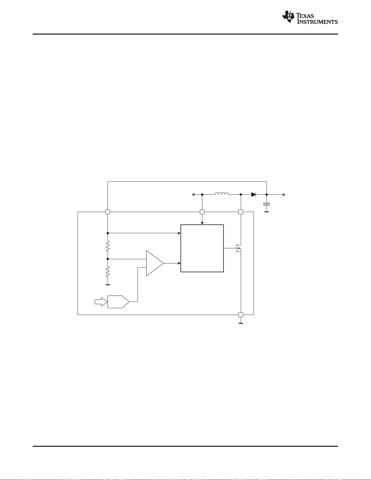
The TPS65154 is a compact LCD bias solution primarily intended for use in Notebook and Tablet PCs.
The device comprises two boost converters to supply the LCD panel's source driver and gate driver; a
linear regulator to supply the system's logic voltage; a programmable V
a gate voltage shaping function; and a 6-channel WLED driver.
• Panel Reset Signal (XAO)
• T-CON Reset Signal (RST)
• On-Chip EEPROM with Write Protect
• I2C Interface
• Thermal Shutdown
• 48-Pin, 6 mm × 6 mm, 0.4 mm Pitch VQFN
TPS65154
SLVSBG2A –SEPTEMBER 2013–REVISED JUNE 2016
with high-speed amplifier; and
COM
spacing
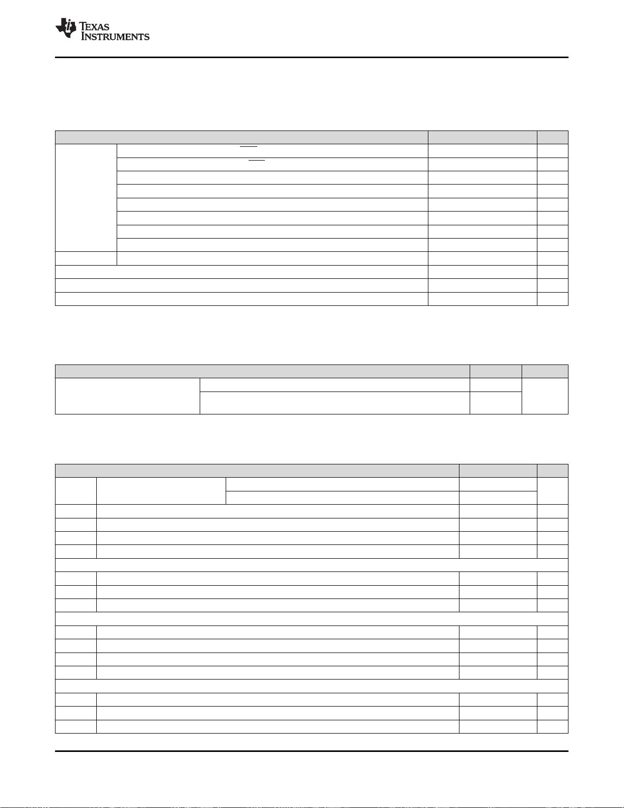
Device Information
PART NUMBER PACKAGE BODY SIZE (NOM)
TPS65154 VQFN (48) 6.00 mm × 6.00 mm
(1) For all available packages, see the orderable addendum at the end of the data manual.
(1)
1.4 Simplified System Diagram
1
An IMPORTANT NOTICE at the end of this data sheet addresses availability, warranty, changes, use in safety-critical applications,
intellectual property matters and other important disclaimers. PRODUCTION DATA.
Page 2
TPS65154
SLVSBG2A –SEPTEMBER 2013–REVISED JUNE 2016
www.ti.com
Table of Contents
1 Device Overview ......................................... 1
1.1 Features .............................................. 1
1.2 Applications........................................... 1
1.3 Description............................................ 1
1.4 Simplified System Diagram........................... 1
2 Revision History ......................................... 2
3 Pin Configuration and Functions..................... 3
4 Specifications ............................................ 5
4.1 Absolute Maximum Ratings .......................... 5
4.2 ESD Ratings.......................................... 5
4.3 Recommended Operating Conditions ................ 5
4.4 Thermal Information .................................. 6
4.5 Electrical Characteristics ............................. 7
4.6 Timing Requirements................................. 9
5 Detailed Description ................................... 12
5.1 Overview ............................................ 12
5.2 Functional Block Diagram........................... 12
5.3 Feature Description ................................. 14
5.4 Device Functional Modes ........................... 22
5.5 Programming........................................ 26
5.6 Register Map ........................................ 38
6 Application and Implementation .................... 63
6.1 Application Information.............................. 63
6.2 Typical Application .................................. 63
7 Power Supply Recommendations .................. 75
8 Layout .................................................... 76
8.1 Layout Guidelines ................................... 76
8.2 Layout Example ..................................... 76
9 Device and Documentation Support ............... 78
9.1 Device Support ...................................... 78
9.2 Receiving Notification of Documentation Updates.. 78
9.3 Community Resources .............................. 78
9.4 Trademarks.......................................... 78
9.5 Electrostatic Discharge Caution..................... 78
9.6 Glossary............................................. 78
10 Mechanical, Packaging, and Orderable
Information .............................................. 79
10.1 Packaging Information .............................. 79
2 Revision History
Changes from Original (September 2013) to Revision A Page
• Changed from data sheet to data manual format ................................................................................ 1
• Added Device Information table, ESD Ratings table, Feature Description section, Device Functional Modes,
Application and Implementation section, Power Supply Recommendations section, Layout section, Device and
Documentation Support section, and Mechanical, Packaging, and Orderable Information section. ...................... 1
2
Revision History Copyright © 2013–2016, Texas Instruments Incorporated
Submit Documentation Feedback
Product Folder Links: TPS65154
Page 3
1
2
3
4
5
6
13
14
15
16
17
18
36
35
34
33
32
31
Thermal Pad
48
47
46
45
44
43
NC
BSUP
AVDD
AVDD
SW1
PGND
NC
VGHM
RE
FLK
VGL
NC
OVP
SW3
PGND
IFB1
IFB2
NC
BGND
COMP1
VCOM
NEG
SCL
7
8
9
10
11
12
VIN
VCC
PGND
SW2
VGH
NC
30
29
28
27
26
25
IFB3
IFB4
IFB5
IFB6
AGND
NC
19
20
21
22
23
24
C1A
C1B
RST
XAO
ISET
NC
42
41
40
39
38
37
SDA
WP
COMP3ENPWM
NC
www.ti.com
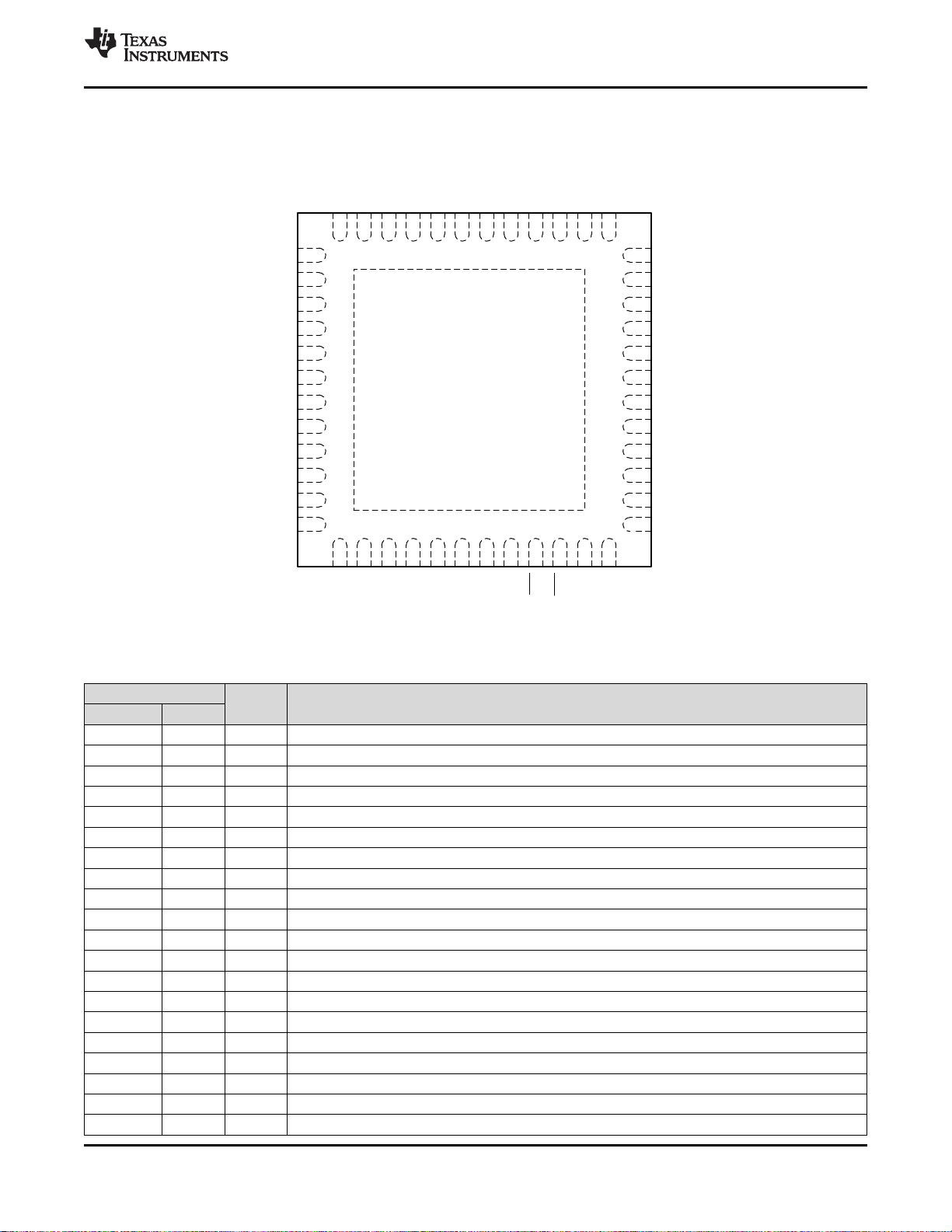
3 Pin Configuration and Functions
TPS65154
SLVSBG2A –SEPTEMBER 2013–REVISED JUNE 2016
Figure 3-1. RSL Package, 48-Pin VQFN (Top View)
Pin Functions
PIN
NAME NO.
NC 1 N/A No internal connection.
BSUP 2 P Positive supply for the VCOM buffer.
AVDD 3 P Boost converter 1 output voltage sense.
AVDD 4 P Boost converter 1 rectifier output.
SW1 5 P Boost converter 1 switch pin.
PGND 6 P Ground.
VIN 7 P Positive supply.
VCC 8 P Linear regulator output.
PGND 9 P Ground.
SW2 10 P Boost converter 2 switch pin.
VGH 11 P VGHregulation point and positive supply for gate voltage shaping function.
NC 12 N/A No internal connection.
NC 13 N/A No internal connection.
VGHM 14 P Gate voltage shaping output.
RE 15 I/O Gate votlage shaping discharge resistor connection.
FLK 16 I/O Gate votlage shaping flicker clock input.
COMP2 17 I/O Internal linear regulator compensation network connection.
VGL 18 P Negative charge pump output and VGLregulation point.
C1A 19 P Negative charge pump flying capacitor connection.
C1B 20 P Negative charge pump flying ccapacitor connection.
TYPE DESCRIPTION
Submit Documentation Feedback
Product Folder Links: TPS65154
Pin Configuration and FunctionsCopyright © 2013–2016, Texas Instruments Incorporated
3
Page 4
TPS65154
SLVSBG2A –SEPTEMBER 2013–REVISED JUNE 2016
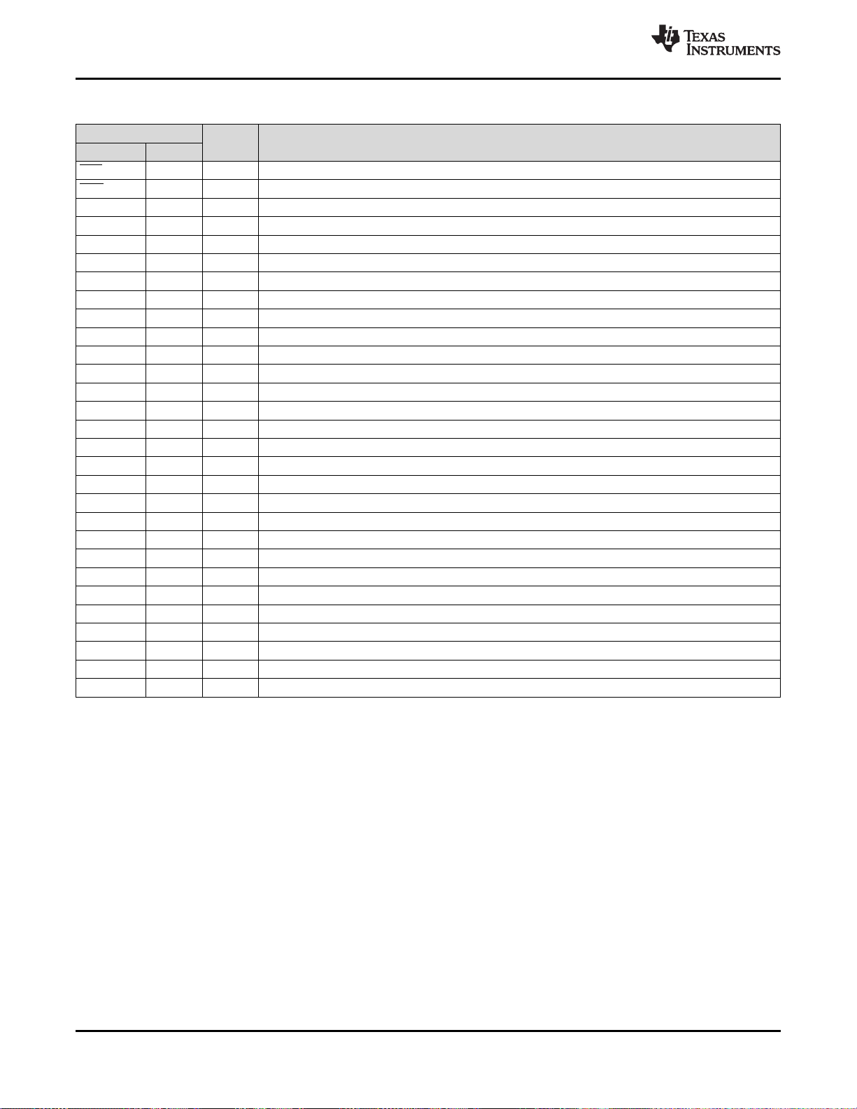
Pin Functions (continued)
PIN
NAME NO.
RST 21 I/O Reset generator output.
XAO 22 I/O Panel discharge generator output.
ISET 23 I/O WLED driver current-setting resistor connection.
NC 24 N/A No internal connection.
NC 25 N/A No internal connection.
AGND 26 P Ground.
IFB6 27 I/O WLED driver channel 6 output.
IFB5 28 I/O WLED driver channel 5 output.
IFB4 29 I/O WLED driver channel 4 output.
IFB3 30 I/O WLED driver channel 3 output.
IFB2 31 I/O WLED driver channel 2 output.
IFB1 32 I/O WLED driver channel 1 output.
PGND 33 P Ground.
SW3 34 P WLED driver boost converter switch pin.
OVP 35 I/O WLED driver boost converter output voltage sensing pin.
NC 36 N/A No internal connection.
NC 37 N/A No internal connection.
PWM 38 I/O WLED driver PWM input.
EN 39 I/O WLED driver enable input.
COMP3 40 I/O WLED driver boost converter compensation network connection.
WP 41 I/O EEPROM write protect input.
SDA 42 I/O I2C data.
SCL 43 I/O I2C clock.
NEG 44 I/O VCOM buffer inverting input.
VCOM 45 I/O VCOM buffer output.
COMP1 46 I/O Boost converter 1 compensation network connection.
BGND 47 P Ground.
NC 48 N/A No internal connection.
GND Pad P Ground.
TYPE DESCRIPTION
www.ti.com
4
Pin Configuration and Functions Copyright © 2013–2016, Texas Instruments Incorporated
Submit Documentation Feedback
Product Folder Links: TPS65154
Page 5
www.ti.com
4 Specifications
TPS65154
SLVSBG2A –SEPTEMBER 2013–REVISED JUNE 2016
4.1 Absolute Maximum Ratings
(1)
over operating free-air temperature range (unless otherwise noted)
MIN MAX UNIT
VIN, VCC, SCL, SDA, FLK, WP, XAO, COMP1 –0.3 7 V
AVDD, SW1, VCOM, NEG, BSUP, RST –0.3 12 V
EN, PWM –0.3 20 V
Pin voltage
COMP2, COMP3, ISET –0.3 3.6 V
C1A, C1B –10 12 V
VGL –10 0.3 V
SW3, OVP –0.3 40 V
IFB1, IFB2, IFB3, IFB4, IFB5, IFB6, VGH, VGHM, RE, SW2 –0.3 30 V
Pin current SW2 TBD A
Ambient temperature, T
Junction temperature, T
Storage temperature, T
A
J
STG
–40 85 °C
–40 150 °C
–65 150 °C
(1) Stresses beyond those listed under “absolute maximum ratings” may cause permanent damage to the device. These are stress ratings
only and functional operation of the device at these or any other conditions beyond those indicated under “recommended operating
conditions” is not implied. Exposure to absolute-maximum-rated conditions for extended periods may affect device reliability.
4.2 ESD Ratings
VALUE UNIT
Human-body model (HBM), per ANSI/ESDA/JEDEC JS-001
V
(ESD)
Electrostatic discharge
Charged-device model (CDM), per JEDEC specification JESD22-
(2)
C101
(1) JEDEC document JEP155 states that 500-V HBM allows safe manufacturing with a standard ESD control process.
(2) JEDEC document JEP157 states that 250-V CDM allows safe manufacturing with a standard ESD control process.
(1)
2000
700
V
4.3 Recommended Operating Conditions
MIN NOM MAX UNIT
V
IN
Input voltage range
dVIN/dt VINrise time 0.45 11 ms
V
V
dV
BSUP
BAT
BAT
Input voltage range 6.5 9.6 V
Input voltage range 4.5 24 V
/dt V
rise time 0.45 11 ms
BAT
LINEAR REGULATOR (VCC)
V
I
C
CC
ICC
OUT
Output voltage 1.0 2.5 V
Output current 300 mA
Output capacitance 4.7 10 22 µF
BOOST CONVERTER 1 (AVDD)
AV
IAV
DD
Boost converter 1 output voltage range 6.5 9.6 V
Boost converter 1 output current at VIN= 3.7 V 400 mA
DD
L Inductance 4.7 10 15 µH
C
OUT
Boost converter 1 output capacitance 4.7 10 22 µF
BOOST CONVERTER 2 (VGH)
AV
V
I
GH
DD
GH
Input voltage range 6.5 9.6 V
Output voltage range 18 25.5 V
Output current 25 mA
Normal operation 2.0 5.5
EEPROM programming 2.6 5.5
V
Submit Documentation Feedback
Product Folder Links: TPS65154
SpecificationsCopyright © 2013–2016, Texas Instruments Incorporated
5
Page 6
TPS65154
SLVSBG2A –SEPTEMBER 2013–REVISED JUNE 2016
www.ti.com
Recommended Operating Conditions (continued)
MIN NOM MAX UNIT
L Inductance 4.7 10 15 µH
C
OUT
Output capacitance 1 4.7 10 µF
NEGATIVE CHARGE PUMP (VGL)
V
GL
I
GL
C
FLY
C
OUT
Output voltage –5 –8 V
Output current 25 mA
Flying capacitance 0.5 µF
Output capacitance 0.5 5 µF
BOOST CONVERTER 3 (WLED)
V
I
OUT
OUT
Output voltage 38 V
Output current 250 mA
L Inductance 4.7 10 15 µH
C
OUT
Output capacitance 2.2 4.7 10 µF
INTERNAL REGULATOR
C
OUT
Capacitance connected to the TCOMP pin 1 µF
4.4 Thermal Information
TPS65154
THERMAL METRIC
R
θJA
R
θJC(top)
R
θJB
ψ
JT
ψ
JB
R
θJC(bot)
Junction-to-ambient thermal resistance 29.8 °C/W
Junction-to-case (top) thermal resistance 15.8 °C/W
Junction-to-board thermal resistance 5.2 °C/W
Junction-to-top characterization parameter 0.2 °C/W
Junction-to-board characterization parameter 5.1 °C/W
Junction-to-case (bottom) thermal resistance 0.8 °C/W
(1) For more information about traditional and new thermal metrics, see Semiconductor and IC Package Thermal Metrics application report.
(1)
UNITRSL (VQFN)
48 PIN
6
Specifications Copyright © 2013–2016, Texas Instruments Incorporated
Submit Documentation Feedback
Product Folder Links: TPS65154
Page 7
www.ti.com
4.5 Electrical Characteristics
VIN= 3.3 V, V
(unless otherwise noted).
POWER SUPPLY
I
IN
I
AVDD
I
BSUP
I
GH
UNDERVOLTAGE LOCKOUT
V
UVLO
LINEAR REGULATOR (VCC)
V
CC
V
UVP
V
SCP
I
LIM
r
DS(ON)
BOOST CONVERTER 1 (AVDD)
AV
DD
V
UVP
V
SCP
r
DS(ON)
I
LIM
r
DS(ON)
f
SW
NEGATIVE CHARGE PUMP (VGL)
V
GL
V
UVP
V
SCP
I
DRVN
V
DO
f
SW
r
DS(ON)
BOOST CONVERTER 2 (VGH)
V
GH
V
UVP
V
SCP
r
DS(ON)
t
ON(MAX)
t
OFF
BOOST CONVERTER 3
V
OUT
I
LIM
r
DS(ON)
= 12 V, VCC= 2.5 V, AVDD= 8 V, VGL= –6.8 V, VGH= 20 V, TA= −40°C to 85°C. Typical values are at 25°C
LED
PARAMETER TEST CONDITIONS MIN TYP MAX UNIT
Supply current into VIN pin Converters not switching 0.1 1 mA
Supply current into AVDD pins Pins 2 and 3 connected together 0.75 2.5 mA
Supply current into BSUP pin 2.5 5 mA
Supply current into VGH pin No load on VGHM 0.1 1 mA
Undervoltage lockout threshold
Hysteresis 90 mV
Linear regulator output voltage range 1.0 2.5 V
Tolerance ICC= 10 mA –3% +3%
Undervoltage protection threshold VCCfalling 60% 70% 75%
Short circuit protection threshold VCCfalling 25% 30% 40%
Current limit VCC= 5% below value at 10 mA.
Active pull-down resistance 10 21 35 Ω
Output voltage range 6.5 9.6 V
Tolerance –2% +2%
Undervoltage protection threshold 60% 70% 75%
Short-circuit protection threshold 25% 30% 35%
Switch ON resistance ISW= 1 A 0.1 0.25 Ω
Switch current limit 2.4 3.0 3.6 A
Rectifier ON resistance ISW= 1 A 0.25 0.4 Ω
Switching frequency 400 1000 kHz
Tolerance –20% +20%
Output voltage range –5 –8 V
Output voltage tolerance –3% 3.5%
Undervoltage protection threshold VGLrising 65% 70% 75%
Short-circuit protection threshold VGLrising 25% 30% 35%
Maximum drive current
Dropout voltage fSW= 500 kHz, C
Switching frequency 400 500 600 kHz
Discharge ON resistance I
Output voltage range 18 25.5 V
Tolerance –3% 3%
Undervoltage protection threshold VGHfalling 65% 70% 75%
Short-circuit protection threshold VGHfalling 25% 30% 35%
Switch ON resistance ISW= 1 A 0.3 1.0 Ω
Maximum tONtime 1 2 2.5 µs
t
time 2 2.7 4 µs
OFF
Output voltage range V
Switch current limit 2.0 2.7 3.7 A
Switch ON resistance ISW= 1 A 0.2 0.35 Ω
SLVSBG2A –SEPTEMBER 2013–REVISED JUNE 2016
VINfalling 1.75
VINrising 2.2
TJ= 25°C to 125°C 300
TJ= –40°C 250
C1B sinking 50 150
C1B sourcing 60 160
= 0.5 µF, IGL= 10 mA 0.6 1.0 V
FLY
= 2 mA 2.1 3 3.9 kΩ
MEAS
+2 38 V
LED
TPS65154
V
mA
mA
Submit Documentation Feedback
Product Folder Links: TPS65154
SpecificationsCopyright © 2013–2016, Texas Instruments Incorporated
7
Page 8

TPS65154
SLVSBG2A –SEPTEMBER 2013–REVISED JUNE 2016
www.ti.com
Electrical Characteristics (continued)
VIN= 3.3 V, V
(unless otherwise noted).
V
OVP
V
IL
V
IH
VIH– VILEN input hysteresis 0.09 0.16 0.27 V
R
PULL-
DOWN
WLED DIMMING
I
FB
D
MIN
D
HYS
V
SET
K
SET
V
IL
V
IH
VIH– VILPWM input voltage hysteresis 0.09 0.16 0.27 V
R
PULL-
DOWN
RESET (RST)
V
OL
I
OH
PROGRAMMABLE VCOM
SET
ZSE
SET
FSE
DNL Differential nonlinearity
BW Small-signal bandwidth
I
OUT
SR Slew rate
I
IB–
V
DROP
GATE VOLTAGE SHAPING
r
DS(ON)H
r
DS(ON)L
V
IL
V
IH
VIH– VILFLK input hysteresis 0.09 0.15 0.27 V
= 12 V, VCC= 2.5 V, AVDD= 8 V, VGL= –6.8 V, VGH= 20 V, TA= −40°C to 85°C. Typical values are at 25°C
LED
PARAMETER TEST CONDITIONS MIN TYP MAX UNIT
OVP range 30 39 V
Tolerance -5% +5%
EN low input voltage ENfalling 0.6 V
EN high input voltage EN rising 1.5 V
EN pull-down resistance 450 750 1250 kΩ
Maximum current 40 mA
Channel-to-channel current matching –3% +3%
Output dimming resolution 10 bits
Minimum output duty cycle 1%
Input PWM jitter hysteresis
–0.048
%
0.048
%
ISET regulation voltage –3% 1.0 +3% V
ISET multiplication constant 1260 1296 1332
PWM low input voltage PWM falling 0.6 V
PWM high input voltage PWM rising 1.2 V
PWM pull-down resistance 450 750 1250 kΩ
Output voltage I
Leakage current V
VCOM DAC set zero-scale error V
= 1 mA (sinking) 0.2 0.5 V
RST
= 1.8 V 1 µA
RST
MIN
= 07h, V
= 07h −7 7
MAX
VMIN DAC set zero-scale error –1 1
VCOM set full-scale error V
MIN
= 07h, V
= 07h −7 7
MAX
VMIN set full-scale error −1 1
V
COM
MAX
V
MIN
Closed-loop; AV= –1; RF= 1 kΩ, RIN= 1 kΩ, VCM= 4 V; V
= 63 mVpp; RL= ∞
Peak output current
Open-loop; V
Open-loop; V
Open-loop; V
Open-loop; V
POS
POS
POS
POS
= 4 V, V
= 4 V, V
= 4 V, V
= 4 V, V
= 3 V 400
NEG
= –5 V 330
NEG
= 5 V 36
NEG
= 3 V 33
NEG
Input bias current (inverting input) Closed-loop; AV= +1; RF= 1 MΩ; V
Output voltage drop
Open-loop; V
10 mA
VGH to VGHM ON resistance VGH= 20 V, I
V
= 20 V, I
VGHM to RE ON resistance
FLK low input voltage threshold V
FLK high input voltage threshold V
GHM
V
= 6 V, I
GHM
falling 0.6 V
FLK
rising 1.2 V
FLK
= 4 V; I
POS
= 10 mA, V
GHM
GHM
= 10 mA, V
GHM
MEAS
= 10 mA, V
=
= 1.8 V 13 25 Ω
FLK
FLK
= 0 V 26 50
FLK
SIGNAL
= 4 V −1 1 μA
POS
V
= 3 V 0.06 0.1
NEG
V
= 5 V 0.03 0.1
NEG
= 0 V 26 50
1
1
1
21 MHz
LSBVMAX DAC set zero-scale error –1 1
LSBVMAX set full-scale error –1 1
LSBV
mA
V/µs
V
Ω
8
Specifications Copyright © 2013–2016, Texas Instruments Incorporated
Submit Documentation Feedback
Product Folder Links: TPS65154
Page 9

TPS65154
www.ti.com
SLVSBG2A –SEPTEMBER 2013–REVISED JUNE 2016
Electrical Characteristics (continued)
VIN= 3.3 V, V
(unless otherwise noted).
I
IL
I
IH
PANEL RESET (XAO)
V
OL(XAO)
I
LK(XAO)
V
DET
I2C INTERFACE
ADDR
V
IL
V
IH
VIH– VILInput hysteresis 0.05 V
V
OL
C
I
C
B
EEPROM
V
IL
V
IH
VIH– VILWP input voltage hysteresis 0.03 0.05 0.1 V
R
PULL-UP
N
WRITE
THERMAL SHUTDOWN
T
SD
= 12 V, VCC= 2.5 V, AVDD= 8 V, VGL= –6.8 V, VGH= 20 V, TA= −40°C to 85°C. Typical values are at 25°C
LED
PARAMETER TEST CONDITIONS MIN TYP MAX UNIT
FLK low input current V
FLK high input current V
Output voltage I
Leakage current V
XAO Threshold voltage range
Tolerance –3% +3%
= 0 V –100 100 nA
FLK
= 1.8 V –100 100 nA
FLK
= 1 mA (sinking) 0.16 0.5 V
XAO
= 1.8 V 1 µA
XAO
VINfalling
V
UVLO
3.0 V
Hysteresis VINrising 0.05 0.3 V
Configuration parameters slave address 74h
Programmable VCOM slave address 28h
Low level input voltage SCL or SDA falling, standard and fast modes 0.6 V
High level input voltage SCL or SDA rising, standard and fast modes 1.0 V
Low level output voltage Sinking 3 mA 0.36 V
Input capacitance 10 pF
Capacitive load on SDA and SCL
Standard mode 400
Fast mode 400
WP low input voltage threshold VWPfalling 0.8 V
WP high input voltage threshold VWPrising 1.2 V
WP internal pull-up resistor 20 60 100 kΩ
Number of write cycles 1000
Data retention Storage temperature = 150 °C 100 1000 hrs
Thermal shutdown temperature 150
Thermal shutdown hysteresis 10
pF
°C
4.6 Timing Requirements
VIN= 3.3 V, V
(unless otherwise noted).
LINEAR REGULATOR (VCC)
t
DLY1
BOOST CONVERTER 1 (AVDD)
t
SS2
t
DLY2
NEGATIVE CHARGE PUMP (VGL)
t
SS3
t
DLY3
BOOST CONVERTER 2 (VGH)
= 12 V, VCC= 2.5 V, AVDD= 8 V, VGL= –6.8 V, VGH= 20 V, TA= −40°C to 85°C. Typical values are at 25°C
LED
Linear regulator start-up delay time 0 75 ms
Tolerance –20% 30%
Boost converter 1 soft-start duration range 0.5 75 ms
Tolerance –20% 30%
Boost converter 1 start-up delay range 0 75 ms
Tolerance –20% 30%
Negative charge pump soft-start duration 0 35 ms
Tolerance –20% 30%
Negative charge pump start-up delay 0 35 ms
Tolerance –20% 30%
Submit Documentation Feedback
Product Folder Links: TPS65154
MIN TYP MAX UNIT
SpecificationsCopyright © 2013–2016, Texas Instruments Incorporated
9
Page 10
TPS65154
SLVSBG2A –SEPTEMBER 2013–REVISED JUNE 2016
Timing Requirements (continued)
VIN= 3.3 V, V
(unless otherwise noted).
t
SS4
BOOST CONVERTER 3
f
SW
WLED DIMMING
t
PWMIN
f
OUT
f
IN
RESET (RST)
t
RST
GATE VOLTAGE SHAPING
t
PLH
t
PHL
t
DLY4
PANEL RESET (XAO)
t
DLY6
TIMING
t
UVP
I2C INTERFACE
f
SCL
t
LOW
t
HIGH
t
BUF
t
hd:STA
t
su:STA
t
su:DAT
t
hd:DAT
= 12 V, VCC= 2.5 V, AVDD= 8 V, VGL= –6.8 V, VGH= 20 V, TA= −40°C to 85°C. Typical values are at 25°C
LED
Boost converter 2 soft-start duration range 0 35 ms
Tolerance –20% 30%
Switching frequency range 400 1000 kHz
Tolerance –20% 20%
Input pulse width 500 ns
Output frequency range
Direct dimming 0.1 15
DPWM dimming 15 22
Tolerance –20% 20%
Input frequency range PWM and direct dimming modes 0.1 15 kHz
Reset pulse duration range 0 15 ms
Tolerance
Measured from end of VCC's ramp to 50% of
RST's rising edge with a 10 kΩ pull-up resistor.
V
Propagation delay
C
V
C
Gate voltage shaping start-up delay range 0 35 ms
Tolerance –20% 30%
Panel reset duration range 0 35 ms
Tolerance
Measured from VIN= V
rising edge with a 10-kΩ pull-up resistor.
Undervoltage protection timeout 40 50 60 ms
Clock frequency
Clock low period
Clock high period
Bus free time between a
STOP and a START
condition
Hold time for a repeated
START condition
Set-up time for a repeated
START condition
Data set-up time
Data hold time
Standard mode 100
Fast mode 400
Standard mode 4.7
Fast mode 1.3
Standard mode 4.0
Fast mode 0.6
Standard mode 4.7
Fast mode 1.3
Standard mode 4.0
Fast mode 0.6
Standard mode 4.0
Fast mode 0.6
Standard mode 250
Fast mode 100
Standard mode 0.05 3.45
Fast mode 0.05 0.9
rising, V
GHM
= 150 pF, RE= 0 Ω
VGHM
falling, V
GHM
= 150 pF, RE= 0 Ω
VGHM
= 0 V/1.8 V, 50% thresholds,
FLK
=0 V/1.8 V, 50% thresholds,
FLK
to 50% of XAO's
DET
www.ti.com
MIN TYP MAX UNIT
–20% 20%
92 200
88 200
–20% 30%
kHz
ns
kHz
µs
µs
µs
µs
µs
ns
µs
10
Specifications Copyright © 2013–2016, Texas Instruments Incorporated
Submit Documentation Feedback
Product Folder Links: TPS65154
Page 11
www.ti.com
Timing Requirements (continued)
VIN= 3.3 V, V
(unless otherwise noted).
t
RCL1
t
RCL
t
FCL
t
RDA
t
FDA
t
su:STO
EEPROM
t
WRITE
= 12 V, VCC= 2.5 V, AVDD= 8 V, VGL= –6.8 V, VGH= 20 V, TA= −40°C to 85°C. Typical values are at 25°C
LED
Rise time of SCL after a
repeated START condition
and after an ACK bit
Rise time of SCL
Fall time of SCL
Rise time of SDA
Fall time of SDA
Set-up time for STOP
condition
Standard mode 20+0.1C
Fast mode 20+0.1C
Standard mode 20+0.1C
Fast mode 20+0.1C
Standard mode 20+0.1C
Fast mode 20+0.1C
Standard mode 20+0.1C
Fast mode 20+0.1C
Standard mode 20+0.1C
Fast mode 20+0.1C
Standard mode 4.0
Fast mode 0.6
Write time 100 ms
TPS65154
SLVSBG2A –SEPTEMBER 2013–REVISED JUNE 2016
MIN TYP MAX UNIT
B
B
B
B
B
B
B
B
B
B
1000
1000
1000
300
300
300
1000
300
300
300
ns
ns
ns
ns
ns
µs
Submit Documentation Feedback
Product Folder Links: TPS65154
SpecificationsCopyright © 2013–2016, Texas Instruments Incorporated
11
Page 12

TPS65154
SLVSBG2A –SEPTEMBER 2013–REVISED JUNE 2016
5 Detailed Description
5.1 Overview
The TPS65154 device integrates the bias and backlight functions needed by an active matrix liquid crystal
display.
The LCD bias functions comprise
• A synchronous boost converter to generate AV
• A non-synchronous boost converter to generate V
• An inverting charge pump to generate V
• An low dropout linear regulator to generate V
• A gate-voltage shaping function
• A programmable VCOM buffer
• XAO and RST signals
• An I2C programming interface
The backlight driver functions comprise
• A non-synchronous boost converter
• A six-channel WLED driver with PWM dimming
www.ti.com
DD
GH
GL
CC
The device configuration is stored in an on-chip nonvolatile memory, which can be programmed via an I2C
interface.
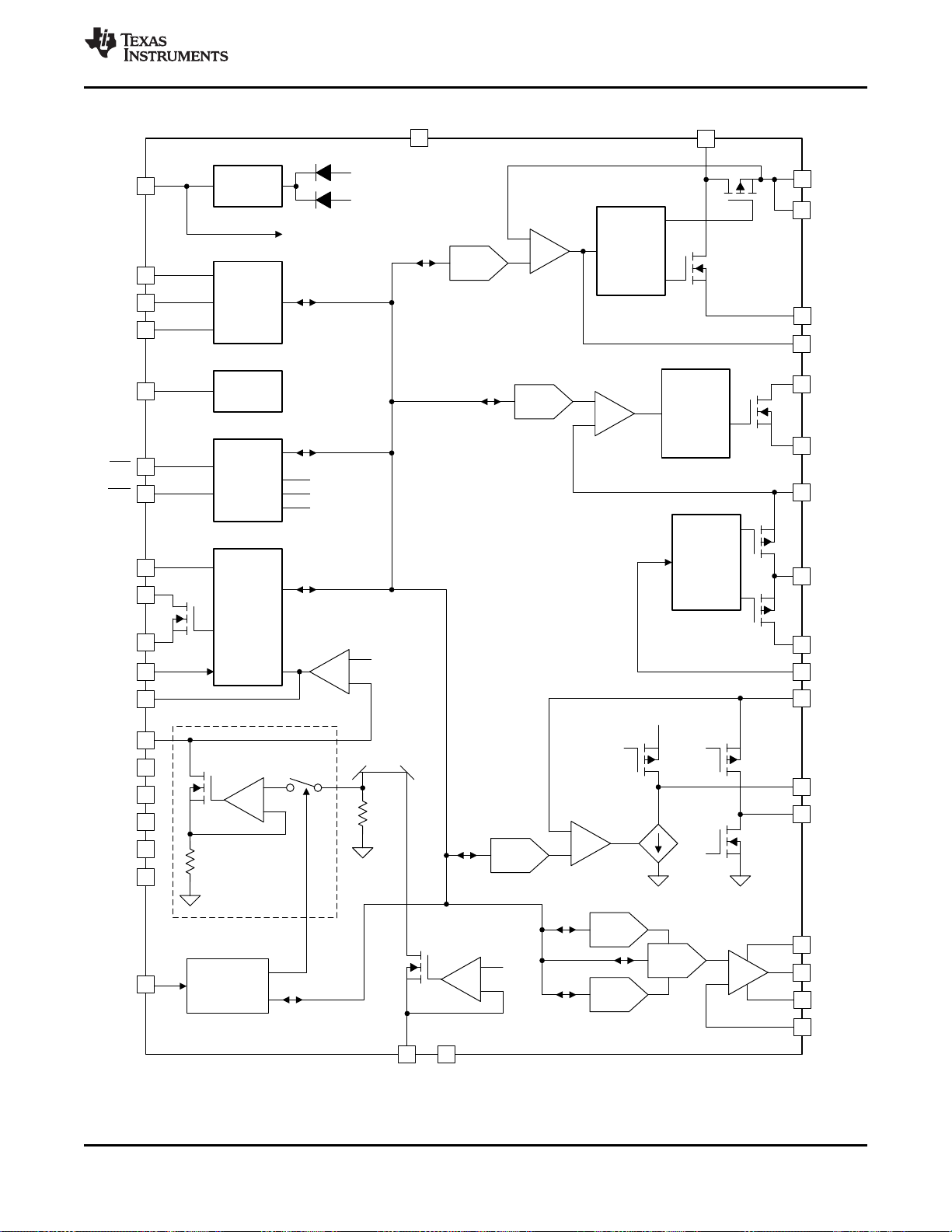
5.2 Functional Block Diagram
Figure 5-1 shows a top-level block diagram of the TPS65154.
12
Detailed Description Copyright © 2013–2016, Texas Instruments Incorporated
Submit Documentation Feedback
Product Folder Links: TPS65154
Page 13
PWM
Control
6
3
5
DAC
+
±
46
4
PWM
Control
9
10
DAC +
±
14
15
Gate
Voltage
Shaping
Control
16
11
I2C
Interface
41
42
43
WP
SDA
SCL
LDO
1920C1A
C1B
VGL
DAC +
±
18
VCOM
BSUP
BGND
NEG
2
47
44
45
+
±
DAC
DAC
DAC
AV
DD
8VCC
LDO17COMP2
To internal blocks
V
IN
AV
DD
Sequencing
21
22
RST
XAO
V
IN
V
UVLO
V
DET
32IFB1
31IFB2
30IFB3
29IFB4
28IFB5
27IFB6
PWM
Control
33
34
+
±
SW3
PGND
39EN
40COMP3
35OVP
V
ref
+±1 V
23
+
±
Only one channel
shown in detail
FLK
RE
VGHM
VGH
PGND
SW2
COMP1
PGND
AVDD
AVDD
SW1
ISET26AGND
7
VIN
Dimming
Control
37PWM
Copyright © 2016, Texas Instruments Incorporated
www.ti.com
TPS65154
SLVSBG2A –SEPTEMBER 2013–REVISED JUNE 2016
Figure 5-1. Top-Level Block Diagram
Submit Documentation Feedback
Product Folder Links: TPS65154
Detailed DescriptionCopyright © 2013–2016, Texas Instruments Incorporated
13
Page 14
VIN
+
–
C
OUT
VCC
V
CC
DAC
VCC
Copyright © 2016, Texas Instruments Incorporated
TPS65154
SLVSBG2A –SEPTEMBER 2013–REVISED JUNE 2016
5.3 Feature Description
The following sections describe the features of the TPS65154.
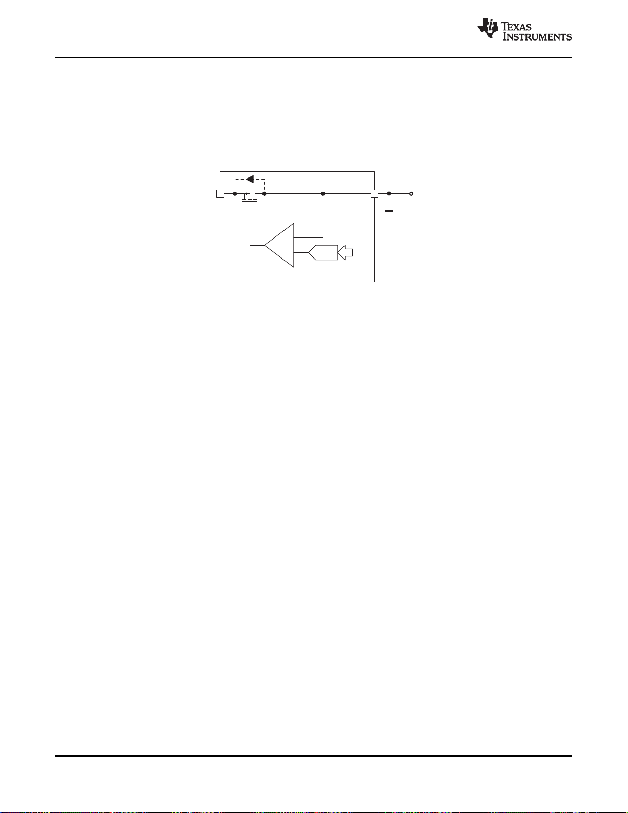
5.3.1 Linear Regulator (VCC)
The linear regulator is supplied directly from the VIN pin, and its output voltage can be programmed to
1.0 V, 1.2 V, 1.89 V, or 2.5 V using the VCC register.
Figure 5-2. Linear Regulator Block Diagram
www.ti.com
5.3.1.1 Power-Up (Linear Regulator)
The linear regulator starts t
threshold (VIN> V
). It does not have a soft-start function, and its output ramps up as fast as the
UVLO
milliseconds after the supply voltage exceeds the undervoltage lockout
DLY1
supply voltage slew rate and the linear regulator's output capacitance allow.
5.3.1.2 Power-Down (Linear Regulator)
The linear regulator is turned off as soon as the supply voltage falls below the undervoltage lockout
threshold (VIN< V
). VCCis actively discharged during power-down.
UVLO
5.3.1.3 Protection (Linear Regulator)
The linear regulator is protected against short-circuits and undervoltage conditions. An undervoltage
condition is detected if the linear regulator's output falls below 70% of its programmed voltage for longer
than 50 ms, in which case the IC is disabled. A short-circuit condition is detected if the linear regulator's
output falls below 30% of its programmed voltage, in which case the IC is disabled immediately (shortcircuit detection has no time delay associated with it). To recover normal operation following either an
undervoltage condition or short-circuit condition, the cause of the error must be removed and a POR
applied.
5.3.2 Boost Converter 1 (AVDD)
Boost converter 1 is synchronous and uses a virtual current mode topology that:
• achieves high efficiencies;
• allows the converter to work in continuous conduction mode under all operating conditions, simplifying
compensation; and
• provides true input-output isolation when the boost converter is disabled.
14
Detailed Description Copyright © 2013–2016, Texas Instruments Incorporated
Submit Documentation Feedback
Product Folder Links: TPS65154
Page 15
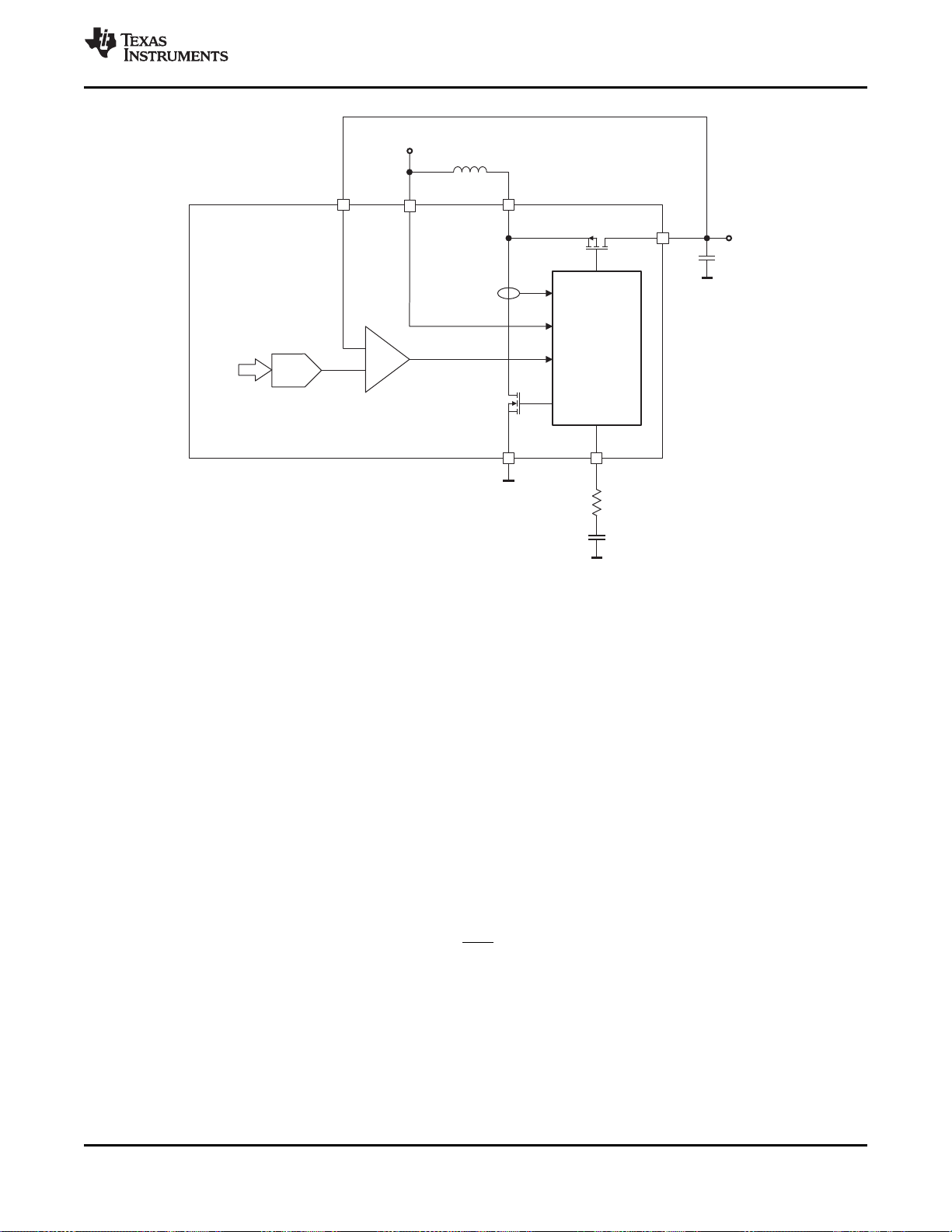
COMP1
SW1
V
IN
AV
DD
Q1B
Q1A
PWM
Control
GND
VIN
L
AVDD
+
–
C
OUT
R
COMP
C
COMP
DAC
AVDD
AVDD
Copyright © 2016, Texas Instruments Incorporated
www.ti.com
TPS65154
SLVSBG2A –SEPTEMBER 2013–REVISED JUNE 2016
Figure 5-3. Boost Converter 1 Internal Block Diagram
Boost converter 1's switching frequency can be programmed to 400 kHz, 600 kHz, 800 kHz, or 1 MHz
using the FSW1 register. Its output voltage can be programmed from 6.5 V to 9.6 V in 100 mV steps using
the AVDD register.
Boost converter 1 uses an external compensation network connected to the COMP1 pin to stabilize its
feedback loop. A simple series R-C network connected between the COMP1 pin and ground is sufficient
to achieve good performance, that is, stable and with good transient response. Good starting values,
which will work for most applications, are 25 kΩ and 3.9 nF.
In some applications (for example, those using electrolytic output capacitors), it may be necessary to
include a second compensation capacitor between the COMP1 pin and ground. This has the effect of
adding an additional pole in the feedback loop's frequency response, which cancels the zero introduced by
the output capacitor's ESR.
The synchronous topology of boost converter 1 ensures that AVDDis fully isolated from VINwhen the
converter is disabled.
5.3.2.1 Power-Up (Boost Converter 1)
Boost converter 1 starts t
milliseconds after RST goes high. Delay time t
DLY2
0 ms to 75 ms using the DLY2 register.
To minimize inrush current during start-up, boost converter 1 ramps its output voltage in t
Start-up time t
can be programmed from 0.5 ms to 75 ms using the SS2 register. Longer soft-start
SS2
times generate lower inrush currents.
5.3.2.2 Power-Down (Boost Converter 1)
can be programmed from
DLY2
milliseconds.
SS2
Boost converter 1 is disabled when VIN<V
AVDDby turning on Q2.
Submit Documentation Feedback
Product Folder Links: TPS65154
. When disabled, boost converter 2 actively discharges
UVLO
Detailed DescriptionCopyright © 2013–2016, Texas Instruments Incorporated
15
Page 16
AV
DD
V
GH
SW2
GND
VGH
PWM
Control
+
–
VGH
AVDD
L
C
OUT
DAC
Copyright © 2016, Texas Instruments Incorporated
TPS65154
SLVSBG2A –SEPTEMBER 2013–REVISED JUNE 2016
5.3.2.3 Protection (Boost Converter 1)
Boost converter 1 is protected against short-circuits and undervoltage conditions. An undervoltage
condition is detected if the boost converter's output falls below 70% of its programmed voltage for longer
than 50 ms, in which case the IC is disabled. A short-circuit condition is detected if the boost converter's
output falls below 30% of its programmed voltage, in which case the IC is disabled immediately (shortcircuit detection has no time delay associated with it). To recover normal operation following either an
undervoltage condition or short-circuit condition, the cause of the error must be removed and a POR
applied.
5.3.3 Boost Converter 2 (VGH)
Boost converter 2 is non-synchronous and uses a constant off-time topology. The converter's switching
frequency is not constant but adapts itself to VINand VGH. Boost converter 2 uses peak current control and
is designed to operate permanently in discontinuous conduction mode (DCM), thereby allowing the
internal compensation circuit to achieve stable operation over a wide range of output voltages and
currents. Boost converter 2's output voltage can be programmed from 18 V to 25.5 V using the VGH
register.
www.ti.com
Figure 5-4. Boost Converter 2 Block Diagram
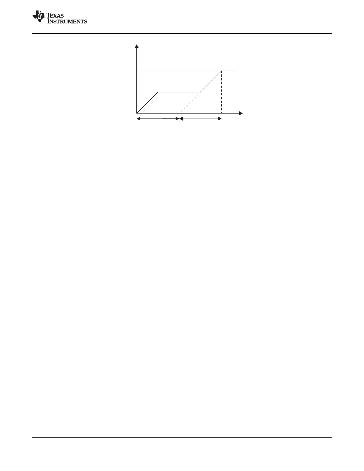
5.3.3.1 Power-Up (Boost Converter 2)
Boost converter 2 is enabled as soon as VGLhas finished ramping down. To minimize inrush current
during start-up, boost converter 2 ramps VGHlinearly to its programmed value in t
16
time t
is non-synchronous, its output is already equal to AVDD(minus the voltage drop across its rectifier diode)
before it starts switching, which means that the time during which VGHis actually ramping during start-up
is less than the actual programmed soft-start time (see Figure 5-5).
Detailed Description Copyright © 2013–2016, Texas Instruments Incorporated
can be programmed from 0.256 ms to 35 ms using the SS4 register. Because boost converter 2
SS4
Submit Documentation Feedback
Product Folder Links: TPS65154
seconds. Soft-start
SS4
Page 17
t
SS4
t + t
DLY3 SS3
V
GH
AV
DD
www.ti.com
Figure 5-5. Boost Converter 2 Soft-Start
5.3.3.2 Power-Down (Boost Converter 2)
TPS65154
SLVSBG2A –SEPTEMBER 2013–REVISED JUNE 2016
Boost converter 2 is disabled when VIN<V
converter is disabled.
5.3.3.3 Protection (Boost Converter 2)
Boost converter 2 is protected against short-circuits and undervoltage conditions. An undervoltage
condition is detected if the boost converter's output falls below 70% of its programmed voltage for longer
than 50 ms, in which case the IC is disabled. A short-circuit condition is detected if the boost converter's
output falls below 30% of its programmed voltage, in which case the IC is disabled immediately (shortcircuit detection has no time delay associated with it). To recover normal operation following either an
undervoltage condition or short-circuit condition, the cause of the error must be removed and a POR
applied.
5.3.4 Negative Charge Pump (VGL)
The negative charge pump inverts AVDDand regulates its output to the voltage set by the VGL register.
VGLcan be programmed from –5 V to –8 V in 0.2 V steps using the VGL register, however, since the
negative charge pump inverts AVDDto generate its output, the most negative voltage that can be
generated is approximately –AVDD+1 V. Thus, if AVDD= 8.0 V, the usable range of VGLis approximately –5
V to –7 V. If VGLis programmed to a more negative voltage than this the charge pump may not be able to
regulate its output. This will not damage the IC, but performance may be impaired.
The negative charge pump in the TPS65154 is fully integrated and requires only two external capacitors to
operate (a flying capacitor connected between the C1A and C1B pins, and an output capacitor connected
between the VGL pin and ground).
. The converter's output is not actively discharged when the
UVLO
Submit Documentation Feedback
Product Folder Links: TPS65154
Detailed DescriptionCopyright © 2013–2016, Texas Instruments Incorporated
17
Page 18
AV
DD
Osc.
V
GL
C
OUT
C
FLY
C1A
C1B
VGL
I
DRVN
VGL
DAC
Copyright © 2016, Texas Instruments Incorporated
TPS65154
SLVSBG2A –SEPTEMBER 2013–REVISED JUNE 2016
Figure 5-6. Negative Charge Pump Block Diagram
5.3.4.1 Power-Up (Negative Charge Pump)
www.ti.com
The negative charge pump starts t
milliseconds after boost converter 1 (AVDD) starts ramping and
DLY3
ramps its output linearly from zero to its programmed output voltage in t
programmed from 0 ms to 35 ms using the DLY3 register. Soft-start time t
0 ms to 35 ms using the SS3 register.
5.3.4.2 Power-Down (Negative Charge Pump)
The negative charge pump is disabled when the supply voltage falls below the undervoltage lockout
threshold (VIN<V
). During power-down the charge pump's output is actively discharge to GND.
UVLO
5.3.4.3 Protection (Negative Charge Pump)
The negative charge pump is protected against short-circuits and undervoltage conditions. An
undervoltage condition is detected if the charge pump's output falls below 70% of its programmed voltage
for longer than 50 ms, in which case the IC is disabled. A short-circuit condition is detected if the charge
pump's output falls below 30% of its programmed voltage, in which case the IC is disabled immediately
(short-circuit detection has no time delay associated with it). To recover normal operation following either
an undervoltage condition or short-circuit condition, the cause of the error must be removed and a POR
applied.
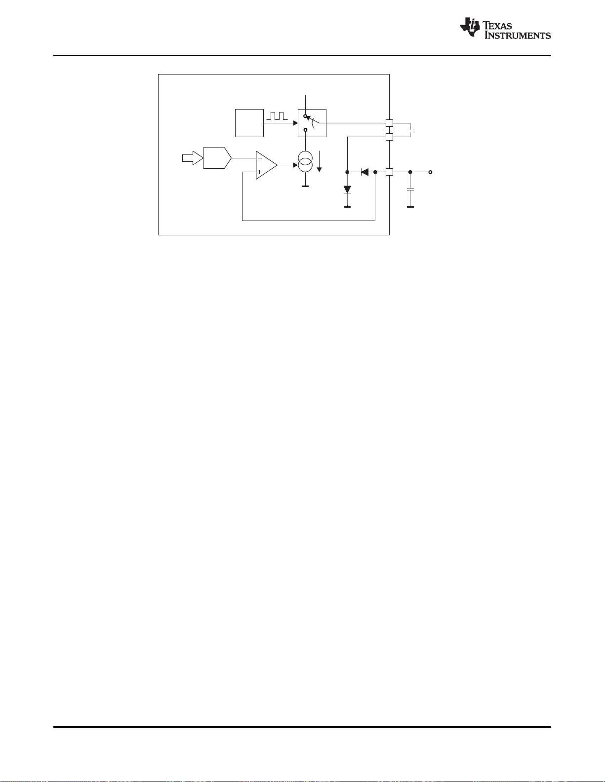
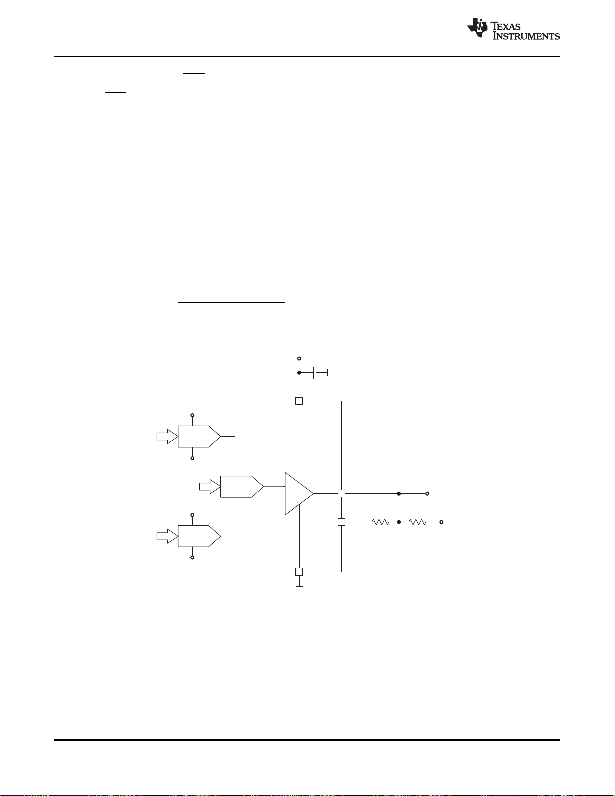
5.3.5 Gate Voltage Shaping
The gate voltage shaping function can be used to reduce image sticking in LCD panels by modulating the
LCD panel's gate ON voltage (VGH). Figure 5-7 shows a block diagram of the gate voltage shaping
function and Figure 5-8 shows the typical waveforms during operation.
ms. Delay time t
SS3
can be programmed from
SS3
DLY3
can be
18
Detailed Description Copyright © 2013–2016, Texas Instruments Incorporated
Submit Documentation Feedback
Product Folder Links: TPS65154
Page 19
Don’t Care
t
DLY4
V
PG4
V
GH
FLK
V
GHM
AV
DD
GND
V
GH
Control
Logic
FLK
V
GHM
R
E
Q1
Q3
AV
DD
Q2
Q4
Copyright © 2016, Texas Instruments Incorporated
www.ti.com
TPS65154
SLVSBG2A –SEPTEMBER 2013–REVISED JUNE 2016
Figure 5-7. Gate Voltage Shaping Block Diagram
Figure 5-8. Gate Voltage Shaping Waveforms
Gate voltage shaping is controlled by the FLK input. When FLK is high, Q1 is on, Q2, Q3 and Q4 are off,
and V
is equal to VGH. On the falling edge of FLK, Q1 is turned off, Q2 and Q3 are turned on, and the
GHM
LCD panel load connected to the VGHM pin discharges through the external resistor connected to the RE
pin.
During power-up, Q1, Q2 and Q3 are held off and Q4 is turned on, pulling the VGHM pin pulled to GND,
regardless of the state of the FLK signal, until t
ramping. The value of t
DLY4
During power-down Q1 is held permanently on and Q2, Q3 and Q4 permanently off, regardless of the
state of the FLK signal.
5.3.6 Panel Discharge (XAO)
The TPS65154 provides an output signal via its XAO pin that can be used to drive the outputs of the
display panel's gate driver IC high during power-down. The XAO pin is pulled low whenever VIN<V
V
DET
The XAO output is an open-drain type and requires an external pull-up, typically in the range 10 kΩ to
100 kΩ.
threshold voltage can be configured using the VDET register.
milliseconds after boost converter 2 (VGH) has finished
DLY4
can be programmed from 0 ms to 35 ms using the DLY4 register.
Detailed DescriptionCopyright © 2013–2016, Texas Instruments Incorporated
Submit Documentation Feedback
Product Folder Links: TPS65154
DET
. The
19
Page 20
VCOM
VMAX
DAC
NEG
VCOM
BGND
BSUP
4/8×AV
DD
2/8×AV
DD
DAC
DACVMIN
2.5/8×AV
DD
3.5/8×AV
DD
V
COM
Feedback from
display panel
AV
DD
+
–
Copyright © 2016, Texas Instruments Incorporated
( )
127
VCOMVV
VV
MINMAX
MINCOM
×-
+=
TPS65154
SLVSBG2A –SEPTEMBER 2013–REVISED JUNE 2016
5.3.7 Reset Generator (RST)
The RST pin generates an active-low reset signal for the rest of the system. During power-up, the reset
timer starts when VCChas finished ramping. The reset pulse duration t
to 15 ms using the RESET register. The RST signal is latched when it goes high and will not be taken low
again until the device is powered down (even if VCCtemporarily falls out of regulation). The active powerdown threshold (V
UVLO
or V
) can be selected using the RMODE bit in the CONFIG register.
DET
The RST output is an open-drain type that requires an external pull-up resistor. Pull-up resistor values in
the range 10 kΩ to 100 kΩ are recommended for most applications.
5.3.8 Programmable VCOM
can be programmed from 0 ms
RST
www.ti.com
The programmable VCOM uses three digital-to-analog converters (DACs) to generate a V
is subsequently buffered by a high-speed op-amp. The maximum value of V
is set by the 4-bit VMAX
COM
register, and can be programmed in the range 2.5/8×AVDDto 4/8×AVDD. The minimum value of V
voltage that
COM
COM
is
set by the 4-bit VMIN register, and can be programmed in the range 2/8 × AVDDto 3.5/8 × AVDD. Note, for
proper operation, V
can adjust the V
COM
must be greater than V
MAX
. By programming the 7-bit VCOM parameter, users
MIN
voltage appearing at the OUT pin between V
MIN
and V
as follows:
MAX
(1)
where VCOM is the value stored in the Wiper Register (see Figure 5-9).
20
Figure 5-9. Programmable VCOM Block Diagram
The programmable VCOM function has three registers. The volatile Wiper Register (WR) contains the
value currently output by the programmable VCOM DAC; this value is lost when power to the device is
removed. The non-volatile Initial Value Register (IVR) contains the value loaded into the DAC every time
the device is powered up. The Control Register (CR) determines whether data is written to or read from
the WR, the IVR, or both. If the CR contains 00h, during write operations data is stored in the WR and the
IVR, and during read operations data is read from the IVR. If the CR contains 80h, data is written to and
read from the WR register only. 00h and 80h are the only valid values for the CR. Table 5-1 shows the
programmable VCOM's register address map.
Detailed Description Copyright © 2013–2016, Texas Instruments Incorporated
Submit Documentation Feedback
Product Folder Links: TPS65154
Page 21

SET
SET
SET
MAX
K
R
V
www.ti.com
Table 5-1. Programmable VCOM Register Address Map
REGISTER ADDRESS NON-VOLATILE VOLATILE
00h Initial Value Register (IVR) Wiper Register (WR)
02h Not Used Control Register (CR)
5.3.8.1 Operational Amplifier Performance
TPS65154
SLVSBG2A –SEPTEMBER 2013–REVISED JUNE 2016
Like most op-amps, the V
op-amp in the TPS65154 is not designed to drive purely capacitive loads, so
COM
it is not recommended to connect a capacitor directly to its output in an attempt to increase performance;
however, the op-amp is capable of delivering high peak currents that make such capacitors unnecessary
in most applications.
High-speed op amps such as the one in the TPS65154 require care when using them. The most common
problem is when parasitic capacitance at the inverting input creates a pole with the feedback resistor,
reducing amplifier stability. Two things can be done to minimize the likelihood of this happening. Both of
these work by shifting the pole (which can never be completely eliminated) to a frequency outside the op
amp's bandwidth, where it has no effect.
• Reduce the value of the feedback resistor. In applications where no feedback from the panel is used,
the feedback resistor can be made zero. In applications where a non-zero feedback resistor has to be
used, a small capacitor (between 10 pF and 100 pF) across the feedback resistor will minimize ringing.
• Minimize the parasitic capacitance at the op amp's inverting input. This is achieved by using short PCB
traces between the feedback resistor and the inverting input, and by removing ground planes and other
copper areas above and below this PCB trace.
5.3.8.2 Power-Up (Programmable VCOM)
The programmable V
is enabled when AVDD> V
COM
5.3.8.3 Power-Down (Programmable VCOM)
During power-down, the programmable VCOM continues to operate until AVDD< V
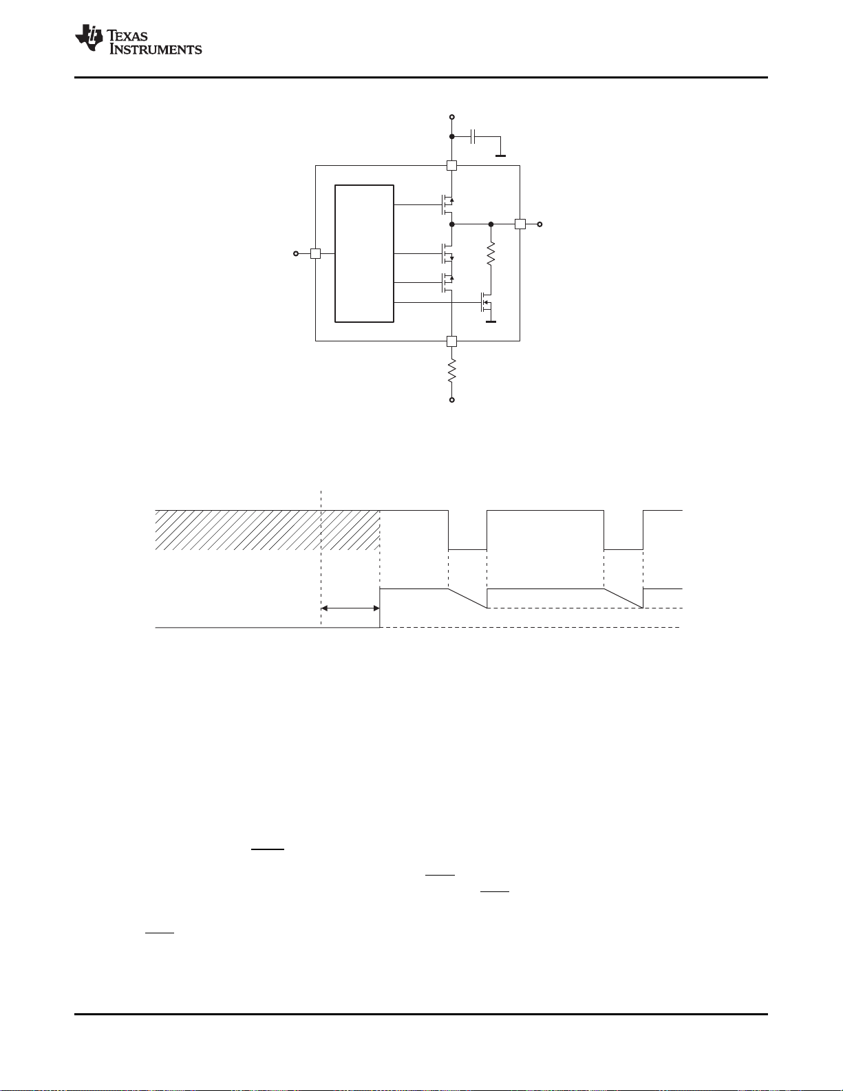
5.3.9 WLED Driver
UVLO2
.
.
UVLO2
5.3.9.1 WLED Boost Converter
The WLED boost converter boosts a 4.5 V to 24 V supply V
strings connected to the WLED driver. It uses a fixed-frequency, current-mode topology. The converter's
output voltage is automatically adjusted to maintain the lowest feedback voltage (IFB1 to IFB6) between
450 mV and 750 mV, thus ensuring sufficient headroom for the output current sinks, but without
dissipating excessive power in the IC. This approach automatically compensates for changes in the LED
string voltage, for example, because of temperature effects. The WLED boost converter's switching
frequency can be programmed to 400 kHz, 600 kHz, 800 kHz, and 1 MHz using the FSW3 register.
The WLED boost converter features a soft-start circuit to limit inrush current when the converter starts.
The duration of the soft-start ramp depends on the value of the capacitor connected to the COMP3 pin.
Note, that because the converter is a non-synchronous type, its output voltage before it starts switching is
equal to V
(minus the voltage drop across its rectifier).
BAT
5.3.9.2 Current Sinks
The brightness of the LED strings is determined by the average current flowing through each string, which
is the product of the output duty cycle and the current sink's output current. The output current of all
current sinks is the same and is set by the external resistor connected between the ISET pin and ground:
Submit Documentation Feedback
Product Folder Links: TPS65154
to a higher voltage to supply the LED
BAT
Detailed DescriptionCopyright © 2013–2016, Texas Instruments Incorporated
(2)
21
Page 22
TPS65154
SLVSBG2A –SEPTEMBER 2013–REVISED JUNE 2016
where:
www.ti.com
• V
• R
• K
is the voltage on the ISET pin
SET
is the resistance between the ISET pin and GND
SET
is a constant
SET
When the TPS65154 measures zero current flowing in one of the IFB pins it determines that the string is
open and automatically disables that output. The WLED boost converter's output voltage is subsequently
regulated according to the remaining operational strings. If an application uses fewer than six LED strings,
it is recommended to connected the unused outputs to ground; this ensures the most rapid detection of
the unused strings. Once open strings have been detected, they remain disabled until a POR occurs or
EN is toggled.
5.3.9.3 Protection
The WLED boost converter and dimming circuits feature a variety of protection schemes to ensure reliable
operation when subjected to various failure modes. These protection schemes are listed in Table 5-2.
ERROR DETECTION ACTION RECOVERY
WLED boost converter output
voltage too high
WLED boost converter switch
current too high
All LED strings open-circuit I
Individual LED string(s) open-
Individual LED string(s) shorted-
circuit
circuited to ground
Table 5-2. WLED Driver Protection
V
exceeds programmed
OVP
threshold
(30 V, 33 V, 36 V or 39 V)
ISW> I
LIM
= 0 mA and V
IFB
I
= 0 mA and V
IFB
I
= 0 mA for longer than 4 ms
IFB
OUT
OUT
= V
= V
OVP
OVP
WLED boost converter output
regulated to programmed
threshold
Switch turned off
Disable all output channels and
boost converter
Disable affected output
channel(s)
Functional output channels
continue operating.
None required
Switch automatically re-enabled
at start of next switching cycle
Output channels re-enabled
following power cycle
Affected output channel(s) re-
enabled following power cycle
5.3.9.4 Enable and Start-Up
The WLED driver is enabled and disabled by EN, however, this signal has no effect until the LCD bias
functions have completed their start-up sequence. Following a POR, EN has no effect until t
complete; after that the WLED driver can be enabled and disabled at any time using EN (providing nothing
happens to cause the LCD bias functions to re-start) and applying a PWM signal. In applications that do
not generate an EN signal, the EN pin can be tied to VIN, in which case the WLED driver will start
automatically at the end of t
boost converter 3 from starting-up.
When the WLED driver is enabled it first checks the status of IFB1 to IFB6 and shuts down any channels
that it detects are disabled/unused. These channels will be subsequently ignored until a POR occurs or
EN is toggled.
5.3.10 Undervoltage Lockout
An undervoltage lockout function disables the IC when the supply voltage is too low for proper operation.
5.4 Device Functional Modes
5.4.1 Dimming Modes
The TPS65154 support direct dimming and phase-shift dimming modes. The active dimming mode can be
selected using the DMODE bit in the CONFIG register.
. Note, that a permanently low PWM signal (0% duty cycle) will prevent
DLY4
DLY4
is
22
Detailed Description Copyright © 2013–2016, Texas Instruments Incorporated
Submit Documentation Feedback
Product Folder Links: TPS65154
Page 23
IFB1
IFB2
IFB3
IFB4
IFB5
IFB6
IFB1
IFB2
IFB3
IFB4
IFB5
IFB6
www.ti.com
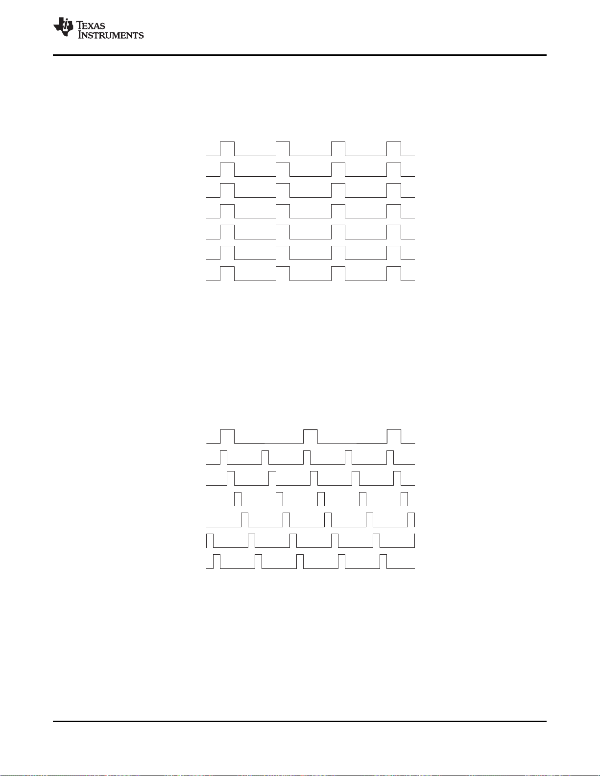
5.4.1.1 Direct Dimming
When direct dimming is selected, the output current sinks are controlled directly by the PWM signal. In this
mode, they are turned on and off together, at the same frequency and duty cycle as the PWM signal (see
Figure 5-10).
5.4.1.2 Phase-Shift Dimming
TPS65154
SLVSBG2A –SEPTEMBER 2013–REVISED JUNE 2016
Figure 5-10. Direct Dimming
When phase-shift dimming mode is selected, the output dimming frequency does not depend on the
frequency of the PWM signal but can be independently programmed from 15 kHz to 22 kHz using the
FDIM register. In this mode, the duty cycle information contained in the PWM signal is extracted and reused to generate up to six outputs, at the output frequency set by the FDIM register, and phase-shifted
with respect to each other by 360°/N, where N is the number of outputs in use (see Figure 5-11). Using
phase-shifted outputs, the maximum load current step is reduced by the same factor N, resulting in
reduced voltage ripple on the boost converter's output and consequently lower audible noise.
Figure 5-11. Phase-Shift Dimming
Submit Documentation Feedback
Product Folder Links: TPS65154
Detailed DescriptionCopyright © 2013–2016, Texas Instruments Incorporated
23
Page 24
TPS65154
SLVSBG2A –SEPTEMBER 2013–REVISED JUNE 2016
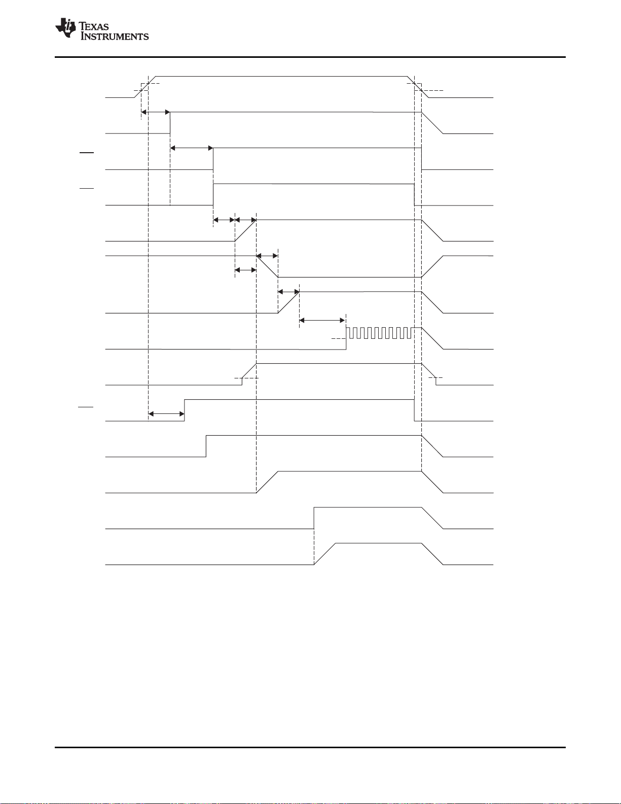
5.4.2 Power Sequencing
Figure 5-12 shows the typical power-up/down characteristic of the TPS65154.
5.4.2.1 Power-Up
www.ti.com
VCCstarts ramping t
RST is initially held low. t
AVDDstarts ramping t
VGLstarts ramping t
VGHstarts ramping as soon as VGLhas finished ramping.
V
is initially held low (connected to RE). t
GHM
shaping is enabled and V
XAO is initially held low. t
The WLED driver is enabled by the logical AND of AVDD(that is, AVDDhas finished ramping) and EN.
5.4.2.2 Power-Down
VCC, AVDD, VGHand VGLare disabled when VIN<V
XAO goes low when VINfalls below the threshold selected for it (V
RST goes low when VINfalls below the threshold selected for it (V
The WLED driver is turned off when EN = 0 or VIN< V
seconds after VIN> V
DLY1
seconds after VCChas finished ramping RST goes high.
RST
seconds after RST has gone high.
DLY2
seconds after AVDDstarts ramping.
DLY3
follows the state of FLK.
GHM
seconds after VIN>V
DLY6
UVLO
DLY4
.
seconds after VGHhas finished ramping, gate voltage
XAO goes high.
DET
.
UVLO
UVLO
or V
UVLO
or V
UVLO
.
DET
DET
).
).
24
Detailed Description Copyright © 2013–2016, Texas Instruments Incorporated
Submit Documentation Feedback
Product Folder Links: TPS65154
Page 25
V
IN
V
CC
t
DLY1
RST
t
DLY2
t
SS2
AV
DD
V
GL
V
GH
t
SS4
t
SS3
V
COM
t
DLY4
V >V
IN DET
AV >V
DD UVLO2
t
DLY3
V >V
IN DET
V >V
IN UVLO1
RST
RMODE=0
RMODE=1
t
RST
EN
V
LED
XAO
V >V
IN UVLO1
AV <V
DD UVLO2
V
GHM
t
DLY6
AV
DD
EN
V
LED
If EN goes high before AV , WLED
boost starts when AV finishes ramping
DD
DD
If EN goes high after AV , WLED
boost starts on rising edge of EN
DD
www.ti.com
TPS65154
SLVSBG2A –SEPTEMBER 2013–REVISED JUNE 2016
Figure 5-12. Power Up/Down Sequencing
Detailed DescriptionCopyright © 2013–2016, Texas Instruments Incorporated
25
Submit Documentation Feedback
Product Folder Links: TPS65154
Page 26

TPS65154
SLVSBG2A –SEPTEMBER 2013–REVISED JUNE 2016
5.5 Programming
5.5.1 Configuration
The TPS65154 divides the configuration parameters into two categories:
• Configuration parameters
• VCOM
In typical applications, all configuration parameters except VCOM are programmed by the subcontractor
during PCB assembly, and VCOM is programmed by the display manufacturer during display calibration.
5.5.1.1 General
Configuration parameters can be changed by writing the desired values to the appropriate RAM
register(s). The RAM registers are volatile and their contents are lost when power is removed from the
device. By writing to the Control Register, it is possible to store the active configuration in non-volatile
EEPROM; during power-up, the contents of the EEPROM are copied into the RAM registers and used to
configure the device.
5.5.1.1.1 I2C Interface
The TPS65154 features an industry-standard I2C interface that supports both Standard and Fast modes of
operation.
www.ti.com
5.5.1.1.2 Slave Addresses
The configuration parameters are all accessed using slave address 74h and the VCOM is accessed using
slave address 28h.
5.5.1.1.3 Write Protect
An active-high Write Protect pin (WP) prevents the configuration parameters from being changed by
accident. This pin is internally pulled high and must be actively pulled low to access to the EEPROM or
RAM registers. Note that the WP pin disables all I2C traffic to the TPS65154, and must also be pulled low
during read operations. This is to ensure that noise present on the I2C lines does not erroneously
overwrite the active configuration stored in RAM (which would not be protected by a simple EEPROM
write-protect scheme). The write protect function can be enabled and disabled using the WPEN bit in the
CONFIG register. Note that once the write protect function is enabled it is not possible to disable again it
without pulling the WP pin low. For this reason, it is strongly recommended that applications include some
way to pull the WP pin low (for example, a test pad), even if it is not normally used.
26
Detailed Description Copyright © 2013–2016, Texas Instruments Incorporated
Submit Documentation Feedback
Product Folder Links: TPS65154
Page 27

S
0
A A7-Bit Slave Address
RAM Register Address
RAM Register Data
A
E8h
P
00h
DATA
www.ti.com
5.5.2 Programming Examples (Excluding VCOM)
5.5.2.1 Writing to a Single RAM Register
1. Bus master sends START condition
2. Bus master sends 7-bit slave address plus low R/W bit (E8h)
3. TPS65154 acknowledges
4. Bus master sends address of RAM register (00h)
5. TPS65154 acknowledges
6. Bus master sends data to be written
7. TPS65154 acknowledges
8. Bus master sends STOP condition
Figure 5-13. Writing to a Single RAM Register
TPS65154
SLVSBG2A –SEPTEMBER 2013–REVISED JUNE 2016
Detailed DescriptionCopyright © 2013–2016, Texas Instruments Incorporated
Submit Documentation Feedback
Product Folder Links: TPS65154
27
Page 28

S
0
A A
7-Bit Slave Address
RAM Register Address (n)
A
P
RAM Register Data (n)
A
E8h
RAM Register Data (n+1)
A
RAM Register Data (Last)
00h
DATA DATA
DATA
TPS65154
SLVSBG2A –SEPTEMBER 2013–REVISED JUNE 2016
5.5.2.2 Writing to Multiple RAM Registers
1. Bus master sends START condition
2. Bus master sends 7-bit slave address plus low R/W bit (E8h).
3. TPS65154 acknowledges
4. Bus master sends address of first RAM register to be written to (00h)
5. TPS65154 acknowledges
6. Bus master sends data to be written to first RAM register
7. TPS65154 acknowledges
8. Bus master sends data to be written to RAM register at next higher address (auto-increment)
9. TPS65154 acknowledges
10. Steps (8) and (9) repeated until data for final RAM register has been sent
11. TPS65154 acknowledges
12. Bus master sends STOP condition
www.ti.com
Figure 5-14. Writing to Multiple RAM Registers
28
Detailed Description Copyright © 2013–2016, Texas Instruments Incorporated
Submit Documentation Feedback
Product Folder Links: TPS65154
Page 29

S
0
A A
7-Bit Slave Address
Control Register Address
Control Register Data
A
E8h
P
FFh
80h
www.ti.com
5.5.2.3 Saving Contents of all RAM Registers to EEPROM
1. Bus master sends START condition
2. Bus master sends 7-bit slave address plus low R/W bit (E8h)
3. TPS65154 acknowledges
4. Bus master sends address of Control Register (FFh)
5. TPS65154 acknowledges
6. Bus master sends data to be written to the Control Register (80h)
7. TPS65154 acknowledges
8. Bus master sends STOP condition
Figure 5-15. Saving Contents of all RAM Registers to EEPROM
TPS65154
SLVSBG2A –SEPTEMBER 2013–REVISED JUNE 2016
Submit Documentation Feedback
Product Folder Links: TPS65154
Detailed DescriptionCopyright © 2013–2016, Texas Instruments Incorporated
29
Page 30

S
0
A A7-Bit Slave Address
Control Register Address
Control Register Data
A
P
S
0
A A
7-Bit Slave Address
RAM Register Address
R/W
Sr
FFh 00h
E8h
E8h
00h
RAM Register Data
7-Bit Slave Address
E9h
1
A
A
P
DATA
TPS65154
SLVSBG2A –SEPTEMBER 2013–REVISED JUNE 2016
5.5.2.4 Reading from a Single RAM Register
1. Bus master sends START condition
2. Bus master sends 7-bit slave address plus low R/W bit (E8h)
3. TPS65154 acknowledges
4. Bus master sends address of Control Register (FFh)
5. TPS65154 acknowledges
6. Bus master sends data for Control Register (00h)
7. TPS65154 acknowledges
8. Bus master sends STOP condition
9. Bus master sends START condition
10. Bus master sends 7-bit slave address plus low R/W bit (E8h)
11. TPS65154 acknowledges
12. Bus master sends address of RAM register (00h)
13. TPS65154 acknowledges
14. Bus master sends REPEATED START condition
15. Bus master sends 7-bit slave address plus high R/W bit (E9h)
16. TPS65154 acknowledges
17. TPS65154 sends RAM register data
18. Bus master does not acknowledge
19. Bus master sends STOP condition
www.ti.com
30
Detailed Description Copyright © 2013–2016, Texas Instruments Incorporated
Figure 5-16. Reading from a Single RAM Register
Submit Documentation Feedback
Product Folder Links: TPS65154
Page 31

S
0
A A
7-Bit Slave Address Control Register Address Control Register Data
A P
S
0
A A
7-Bit Slave Address
EEPROM Register Address
Sr
FFh
01h
E8h
E8h
00h
EEPROM Register Data
7-Bit Slave Address
E9h
1
A
A
P
DATA
www.ti.com
5.5.2.5 Reading from a Single EEPROM Register
1. Bus master sends START condition
2. Bus master sends 7-bit slave address plus low R/W bit (E8h)
3. TPS65154 acknowledges
4. Bus master sends address of Control Register (FFh)
5. TPS65154 acknowledges
6. Bus master sends data for Control Register (01h)
7. TPS65154 acknowledges
8. Bus master sends STOP condition
9. Bus master sends START condition
10. Bus master sends 7-bit slave address plus low R/W bit (E8h)
11. TPS65154 acknowledges
12. Bus master sends address of EEPROM register (00h)
13. TPS65154 acknowledges
14. Bus master sends REPEATED START condition
15. Bus master sends 7-bit slave address plus high R/W bit (E9h)
16. TPS65154 acknowledges
17. TPS65154 sends EEPROM register data
18. Bus master does not acknowledge
19. Bus master sends STOP condition
TPS65154
SLVSBG2A –SEPTEMBER 2013–REVISED JUNE 2016
Figure 5-17. Reading from a Single EEPROM Register
Submit Documentation Feedback
Product Folder Links: TPS65154
Detailed DescriptionCopyright © 2013–2016, Texas Instruments Incorporated
31
Page 32

S
0
A A
7-Bit Slave Address Control Register Address Control Register Data
A P
S
0
A A
7-Bit Slave Address RAM Register Address (n)
R/W
Sr
FFh
00h
E8h
E8h
00h
RAM Register Data (n)
7-Bit Slave Address
E9h
1
A A
DATA
A
RAM Register Data (n+1) RAM Register Data (Last)
A
P
DATADATA
TPS65154
SLVSBG2A –SEPTEMBER 2013–REVISED JUNE 2016
5.5.2.6 Reading from Multiple RAM Registers
1. Bus master sends START condition
2. Bus master sends 7-bit slave address plus low R/W bit (E8h)
3. TPS65154 acknowledges
4. Bus master sends address of Control Register (FFh)
5. TPS65154 acknowledges
6. Bus master sends data for Control Register (00h)
7. TPS65154 acknowledges
8. Bus master sends STOP condition
9. Bus master sends START condition
10. Bus master sends 7-bit slave address plus low R/W bit (E8h)
11. TPS65154 acknowledges
12. Bus master sends address of first register to be read (00h)
13. TPS65154 acknowledges
14. Bus master sends REPEATED START condition
15. Bus master sends 7-bit slave address plus high R/W bit (E9h)
16. TPS65154 acknowledges
17. TPS65154 sends contents of first RAM register to be read
18. Bus master acknowledges
19. TPS65154 sends contents of second RAM register to be read
20. Bus master acknowledges
21. TPS65154 sends contents of third (last) RAM register to be read
22. Bus master does not acknowledge
23. Bus master sends STOP condition
www.ti.com
Figure 5-18. Reading from Multiple RAM Registers
32
Detailed Description Copyright © 2013–2016, Texas Instruments Incorporated
Submit Documentation Feedback
Product Folder Links: TPS65154
Page 33

S
0
A A
7-Bit Slave Address Control Register Address Control Register Data
A P
S
0
A A
7-Bit Slave Address
EEPROM Register Addr (n)
R/W
Sr
FFh
01h
E8h
E8h
00h
EEPROM Register Data (n)
7-Bit Slave Address
E9h
1
A A
DATA
A
EEPROM Register Data (n+1) EEPROM Register Data (Last)
A
P
DATADATA
www.ti.com
5.5.2.7 Reading from Multiple EEPROM Registers
1. Bus master sends START condition
2. Bus master sends 7-bit slave address plus low R/W bit (E8h)
3. TPS65154 acknowledges
4. Bus master sends address of Control Register (FFh)
5. TPS65154 acknowledges
6. Bus master sends data for Control Register (01h)
7. TPS65154 acknowledges
8. Bus master sends STOP condition
9. Bus master sends START condition
10. Bus master sends 7-bit slave address plus low R/W bit (E8h)
11. TPS65154 acknowledges
12. Bus master sends address of first EEPROM register to be read (00h)
13. TPS65154 acknowledges
14. Bus master sends REPEATED START condition
15. Bus master sends 7-bit slave address plus high R/W bit (E9h)
16. TPS65154 acknowledges
17. TPS65154 sends contents of first EEPROM register to be read
18. Bus master acknowledges
19. TPS65154 sends contents of second EEPROM register to be read
20. Bus master acknowledges
21. TPS65154 sends contents of third (last) EEPROM register to be read
22. Bus master does not acknowledge
23. Bus master sends STOP condition
TPS65154
SLVSBG2A –SEPTEMBER 2013–REVISED JUNE 2016
Figure 5-19. Reading from Multiple EEPROM Registers
Submit Documentation Feedback
Product Folder Links: TPS65154
Detailed DescriptionCopyright © 2013–2016, Texas Instruments Incorporated
33
Page 34

S
0
A
0
A
50h 02h
P
Slave Address CR Address
0
A
80h
CR Data
0
0
0
0
0
1
0
1
0
0 0 0 0
0
000
1
0
1
R/W
0
S
0
A
0
A
50h 00h
P
Slave Address
WR Address
1
A
77h
WR Data
0
0
0
0
0
0
0
0
1
1 1 1 1
0
000
1
0
1
R/W
0
TPS65154
SLVSBG2A –SEPTEMBER 2013–REVISED JUNE 2016
5.5.3 Programming Examples - VCOM
5.5.3.1 Writing a VCOM Value of 77h to WR
1. The bus master sends a START condition.
2. The bus master sends 7-bit slave address plus low R/W bit.
3. TPS65154 slave acknowledges.
4. The bus master sends the CR address of 02h.
5. The TPS65154 acknowledges.
6. The bus master sends the CR contents of 80h.
7. The TPS65154 slave acknowledges.
8. The bus master sends a STOP condition.
9. The bus master sends a START condition.
10. The bus master sends 7-bit slave address plus low R/W bit.
11. TPS65154 slave acknowledges.
12. The bus master sends the WR address of 00h.
13. The TPS65154 acknowledges.
14. The bus master sends the WR contents of 77h (right-justified).
15. The TPS65154 slave acknowledges.
16. The bus master sends a STOP condition.
www.ti.com
Figure 5-20. Writing a VCOM Value of 77h to WR
34
Detailed Description Copyright © 2013–2016, Texas Instruments Incorporated
Submit Documentation Feedback
Product Folder Links: TPS65154
Page 35

S
0
A
0
A
50h 02h
P
Slave Address CR Address
0
A
00h
CR Data
0 0 0 0 0
1
0 0 0 0 0 0 00000
1
0
1
R/W
0
S 0
A
0
A
50h 00h
P
Slave Address
WR Address
1 A
77h
WR Data
0 0 0 0 0 0 0 0
1 1 1 1 1
0000
1
0
1
R/W
0
www.ti.com
5.5.3.2 Writing a VCOM Value of 77h to IVR and WR
1. The bus master sends a START condition.
2. The bus master sends 7-bit slave address plus low R/W bit.
3. TPS65154 slave acknowledges.
4. The bus master sends the CR address of 02h.
5. The TPS65154 acknowledges.
6. The bus master sends the CR contents of 00h.
7. The TPS65154 slave acknowledges.
8. The bus master sends a STOP condition.
9. The bus master sends a START condition.
10. The bus master sends 7-bit slave address plus low R/W bit.
11. TPS65154 slave acknowledges.
12. The bus master sends the WR address of 00h.
13. The TPS65154 acknowledges.
14. The bus master sends the WR contents of 77h (right-justified).
15. The TPS65154 slave acknowledges.
16. The bus master sends a STOP condition.
TPS65154
SLVSBG2A –SEPTEMBER 2013–REVISED JUNE 2016
Figure 5-21. Writing a VCOM Value of 77h to IVR and WR
Submit Documentation Feedback
Product Folder Links: TPS65154
Detailed DescriptionCopyright © 2013–2016, Texas Instruments Incorporated
35
Page 36

S
0
A
0
A
50h 02h
P
Slave Address
CR Address
0
A
80h
CR Data
0
0
0
0
0
1
0
1
0
0 0 0 0
0
000
1
0
1
R/W
0
S
0
A
0
A
50h 00h
Slave Address
IVR Address
0
0
0
0
0
0
0
000
1
0
1
R/W
0
S
0
A
0
A
51h 00h
P
Slave Address
WR Data
1
1
1
0
1
1
1
000
1
0
1
R/W
1
Repeated Start
TPS65154
SLVSBG2A –SEPTEMBER 2013–REVISED JUNE 2016
5.5.3.3 Reading a VCOM Value of 77h from WR
1. The bus master sends a START condition.
2. The bus master sends 7-bit slave address plus low R/W bit.
3. TPS65154 slave acknowledges.
4. The bus master sends the CR address of 02h.
5. The TPS65154 acknowledges.
6. The bus master sends the CR contents of 80h.
7. The TPS65154 slave acknowledges.
8. The bus master sends a STOP condition.
9. The bus master sends a START condition.
10. The bus master sends 7-bit slave address plus low R/W bit.
11. TPS65154 slave acknowledges.
12. The bus master sends the WR address of 00h.
13. The TPS65154 acknowledges.
14. The bus master sends a REPEATED START condition.
15. The bus master sends 7-bit slave address plus high R/W bit.
16. The TPS65154 sends the WR contents of 77h (right-justified).
17. The bus master does not acknowledge.
18. The bus master sends a STOP condition.
www.ti.com
36
Detailed Description Copyright © 2013–2016, Texas Instruments Incorporated
Figure 5-22. Reading 77h from WR
Submit Documentation Feedback
Product Folder Links: TPS65154
Page 37

S
0
A
0
A
50h 02h
P
Slave Address
CR Address
0
A
00h
CR Data
0
0
0
0
0
1
0
0
0
0 0 0 0
0
000
1
0
1
R/W
0
S
0
A
0
A
50h 00h
Slave Address
IVR Address
0
0
0
0
0
0
0
000
1
0
1
R/W
0
S
0
A
0
A
51h 00h
P
Slave Address
IVR Data
1
1
1
0
1
1
1
000
1
0
1
R/W
1
Repeated Start
www.ti.com
5.5.3.4 Reading a VCOM Value of 77h from IVR
1. The bus master sends a START condition.
2. The bus master sends 7-bit slave address plus low R/W bit.
3. TPS65154 slave acknowledges.
4. The bus master sends the CR address of 02h.
5. The TPS65154 acknowledges.
6. The bus master sends the CR contents of 00h.
7. The TPS65154 slave acknowledges.
8. The bus master sends a STOP condition.
9. The bus master sends a START condition.
10. The bus master sends 7-bit slave address plus low R/W bit.
11. TPS65154 slave acknowledges.
12. The bus master sends the WR address of 00h.
13. The TPS65154 acknowledges.
14. The bus master sends a REPEATED START condition.
15. The bus master sends 7-bit slave address plus high R/W bit.
16. The TPS65154 sends the WR contents of 77h (right-justified).
17. The bus master does not acknowledge.
18. The bus master sends a STOP condition.
TPS65154
SLVSBG2A –SEPTEMBER 2013–REVISED JUNE 2016
Figure 5-23. Reading 77h from IVR
Submit Documentation Feedback
Product Folder Links: TPS65154
Detailed DescriptionCopyright © 2013–2016, Texas Instruments Incorporated
37
Page 38

TPS65154
SLVSBG2A –SEPTEMBER 2013–REVISED JUNE 2016
5.6 Register Map
5.6.1 Configuration Registers (Excluding VCOM)
Table 5-3 shows the memory map of the configuration parameters.
Table 5-3. Configuration Memory Map
www.ti.com
REGISTER
ADDRESS
00h CONFIG 02h KMODE = 0
01h VCC 03h 2.5 V Sets the output voltage of the linear regulator (VCC)
02h DLY1 02h 10 ms Sets the start-up delay of the linear regulator (VCC)
03h AVDD 0Fh 8.0 V Sets the output voltage of boost converter 1 (AVDD)
04h FSW1 01h 600 kHz Sets the switching frequency of boost converter 1 (AVDD)
05h SS2 04h 20 ms Sets the soft-start time of boost converter 1 (AVDD)
06h DLY2 02h 10 ms Sets the start-up delay of boost converter 1 (AVDD)
07h VGL 09h –6.8 V Sets the output voltage of the negative charge pump (VGL)
08h SS3 01h 5 ms Sets the soft-start time of the negative charge pump (VGL)
09h DLY3 01h 5 ms Sets the start-up delay of the negative charge pump (VGL)
0Ah VGH 04h 20.0 V Sets the output voltage of boost converter 2 (VGH)
0Bh SS4 01h 5 ms Sets the soft-start time of boost converter 2 (VGH)
0Ch FSW3 01h 600 kHz Sets the switching frequency of boost converter 3 (WLED)
0Dh DLY4 02h 10 ms Sets the start-up delay of the gate voltage shaping function (V
0Eh OVP 03h 39 V Sets the over-voltage protection threshold of boost converter 3
0Fh FDIM 07h 22 kHz Sets the output dimming frequency of the WLED driver in phase-shift
10h RESET 05h 5 ms Sets the reset pulse duration
11h VDET 00h V
12h DLY6 02h 30 ms Sets the start-up delay of the XAO signal
13h VMAX 07h 3.2 V Sets the maximum V
14h VMIN 07h 2.7 V Sets the minimum V
15h USER1 00h 00h For customer use
FFh CONTROL 00h Controls whether read and write operations access RAM or EEPROM
REGISTER
NAME
FACTORY DEFAULT DESCRIPTION
WPEN = 0
DMODE = 1
RMODE = 0
= V
DET
UVLO
Sets miscellaneous configuration bits
(WLED)
dimming mode
Sets the threshold of the RST and XAO signals
voltage
COM
voltage
COM
registers
GHM
)
38
Detailed Description Copyright © 2013–2016, Texas Instruments Incorporated
Submit Documentation Feedback
Product Folder Links: TPS65154
Page 39

TPS65154
www.ti.com
SLVSBG2A –SEPTEMBER 2013–REVISED JUNE 2016
5.6.1.1 CONFIG (00h)
The CONFIG register can be written to and read from.
Figure 5-24. CONFIG Register Bit Allocation
7 6 5 4 3 2 1 0
ADIS Reserved KMODE WPEN DMODE RMODE
R/W-0 R/W-0 R/W-0 R/W-0 R/W-0 R/W-0 R/W-1 R/W-0
LEGEND: R/W = Read/Write; R = Read only; -n = factory default
Table 5-4. CONFIG Register Field Descriptions
Bit Field Value Description
7 ADIS This bit can be used to disable boost converter 1 (AVDD), boost converter 2 (VGH) and the negative
6-4 Reserved N/A These bits are reserved for future use and should be programmed to 0 to ensure proper operation.
3 KMODE This bit can be used to enable and disable boost converter 1's active discharge function.
2 WPEN This bit can be used to enable and disable the write protect function.
1 DMODE This bit determines which dimming mode is used by the WLED driver.
0 RMODE This bit determines which threshold is used to assert RST during power-down.
charge pump (VGL) during device programming. This bit is volatile and is never stored in EEPROM.
It is always reset (that is, ADIS = 0) following power-up, that is, the affected converters are always
enabled following power-up.
0 Boost converter 1 (AVDD), boost converter 2 (VGH), and negative charge pump (VGL) enabled.
1 Boost converter 1 (AVDD), boost converter 2 (VGH), and negative charge pump (VGL) disabled.
0 Boost converter 1 (AVDD) active discharge enabled.
1 Boost converter 1 (AVDD) active discharge disabled.
0 Disabled. WP not used and I2C interface always active.
1 Enabled. I2C interface only active when WP pulled low.
0 Direct dimming.
1 Phase-shift dimming.
0 V
1 V
threshold used.
UVLO
threshold used.
DET
Submit Documentation Feedback
Product Folder Links: TPS65154
Detailed DescriptionCopyright © 2013–2016, Texas Instruments Incorporated
39
Page 40

TPS65154
SLVSBG2A –SEPTEMBER 2013–REVISED JUNE 2016
www.ti.com
5.6.1.2 VCC (01h)
The VCC register can be written to and read from.
Figure 5-25. VCC Register Bit Allocation
7 6 5 4 3 2 1 0
Not Implemented VCC
R/W-1 R/W-1
LEGEND: R/W = Read/Write; R = Read only; -n = factory default
Table 5-5. VCC Register Field Descriptions
Bit Field Value Description
7-2 Not implemented N/A These bits are not implemented. During write operations, data for these bits is ignored, and during
1-0 VCC These bits determine the output voltage of the linear regulator (VCC).
read operations 0 is returned.
0h 1.0 V
1h 1.2 V
2h 1.89 V
3h 2.5 V
40
Detailed Description Copyright © 2013–2016, Texas Instruments Incorporated
Submit Documentation Feedback
Product Folder Links: TPS65154
Page 41

TPS65154
www.ti.com
SLVSBG2A –SEPTEMBER 2013–REVISED JUNE 2016
5.6.1.3 DLY1 (02h)
The DLY1 register can be written to and read from.
Figure 5-26. DLY1 Register Bit Allocation
7 6 5 4 3 2 1 0
Not Implemented DLY1
R/W-0 R/W-0 R/W-1 R/W-0
LEGEND: R/W = Read/Write; R = Read only; -n = factory default
Table 5-6. DLY1 Register Field Descriptions
Bit Field Value Description
7-4 Not Implemented N/A These bits are not implemented. During write operations data for these bits is ignored, and during
3-0 DLY1 These bits determine how soon after VIN>V
write operations 0 is returned.
0h 0 ms
1h 5 ms
2h 10 ms
3h 15 ms
4h 20 ms
5h 25 ms
6h 30 ms
7h 35 ms
8h 40 ms
9h 45 ms
Ah 50 ms
Bh 55 ms
Ch 60 ms
Dh 65 ms
Eh 70 ms
Fh 75 ms
the linear regulator (VCC) starts.
UVLO
Submit Documentation Feedback
Product Folder Links: TPS65154
Detailed DescriptionCopyright © 2013–2016, Texas Instruments Incorporated
41
Page 42

TPS65154
SLVSBG2A –SEPTEMBER 2013–REVISED JUNE 2016
5.6.1.4 AVDD (03h)
The AVDD register can be written to and read from.
Figure 5-27. AVDD Register Bit Allocation
7 6 5 4 3 2 1 0
Not Implemented AVDD
R/W-0 R/W-1 R/W-1 R/W-1 R/W-1
LEGEND: R/W = Read/Write; R = Read only; -n = factory default
Table 5-7. AVDD Register Field Descriptions
Bit Field Value Description
1 Not Implemented N/A These bits are not implemented. During write operations data for these bits is ignored, and during
read operations 0 is returned.
0 AVDD These bits determine the output voltage of boost converter 1 (AVDD).
00h 6.5 V
01h 6.6 V
02h 6.7 V
03h 6.8 V
04h 6.9 V
05h 7.0 V
06h 7.1 V
07h 7.2 V
08h 7.3 V
09h 7.4 V
0Ah 7.5 V
0Bh 7.6 V
0Ch 7.7 V
0Dh 7.8 V
0Eh 7.9 V
0Fh 8.0 V
10h 8.1 V
11h 8.2 V
12h 8.3 V
13h 8.4 V
14h 8.5 V
15h 8.6 V
16h 8.7 V
17h 8.8 V
18h 8.9 V
19h 9.0 V
1Ah 9.1 V
1Bh 9.2 V
1Ch 9.3 V
1Dh 9.4 V
1Eh 9.5 V
1Fh 9.6 V
www.ti.com
42
Detailed Description Copyright © 2013–2016, Texas Instruments Incorporated
Submit Documentation Feedback
Product Folder Links: TPS65154
Page 43

TPS65154
www.ti.com
SLVSBG2A –SEPTEMBER 2013–REVISED JUNE 2016
5.6.1.5 FSW1 (04h)
The FSW1 register can be written to and read from.
Figure 5-28. FSW1 Register Bit Allocation
7 6 5 4 3 2 1 0
Not Implemented FSW1
R/W-0 R/W-1
LEGEND: R/W = Read/Write; R = Read only; -n = factory default
Table 5-8. FSW1 Register Field Descriptions
Bit Field Value Description
7-2 Not Implemented N/A These bits are not implemented. During write operations data for these bits is ignored, and during
1-0 FSW1 These bits determine the switching frequency of boost converter 1 (AVDD).
read operations 0 is returned.
0h 400 kHz
1h 600 kHz
2h 800 kHz
3h 1 MHz
Submit Documentation Feedback
Product Folder Links: TPS65154
Detailed DescriptionCopyright © 2013–2016, Texas Instruments Incorporated
43
Page 44

TPS65154
SLVSBG2A –SEPTEMBER 2013–REVISED JUNE 2016
5.6.1.6 SS2 (05h)
The SS2 register can be written to and read from.
Figure 5-29. SS2 Register Bit Allocation
7 6 5 4 3 2 1 0
Not Implemented SS2
R/W-0 R/W-1 R/W-0 R/W-0
LEGEND: R/W = Read/Write; R = Read only; -n = factory default
Table 5-9. SS2 Register Field Descriptions
Bit Field Value Description
7-4 Not Implemented N/A These bits are not implemented. During write operations data for these bits is ignored, and during
read operations 0 is returned.
3-0 SS2 These bits determine the soft-start time of boost converter 1 (AVDD).
0h 0.5 ms
1h 5 ms
2h 10 ms
3h 15 ms
4h 20 ms
5h 25 ms
6h 30 ms
7h 35 ms
8h 40 ms
9h 45 ms
Ah 50 ms
Bh 55 ms
Ch 60 ms
Dh 65 ms
Eh 70 ms
Fh 75 ms
www.ti.com
44
Detailed Description Copyright © 2013–2016, Texas Instruments Incorporated
Submit Documentation Feedback
Product Folder Links: TPS65154
Page 45

TPS65154
www.ti.com
SLVSBG2A –SEPTEMBER 2013–REVISED JUNE 2016
5.6.1.7 DLY2 (06h)
The DLY2 register can be written to and read from.
Figure 5-30. DLY2 Register Bit Allocation
7 6 5 4 3 2 1 0
Not Implemented DLY2
R/W-0 R/W-0 R/W-1 R/W-0
LEGEND: R/W = Read/Write; R = Read only; -n = factory default
Table 5-10. DLY2 Register Field Descriptions
Bit Field Value Description
7-4 Not Implemented N/A These bits are not implemented. During write operations data for these bits is ignored, and during
3-0 DLY2 These bits determine how soon after RST goes high boost converter 1 (AVDD) starts.
read operations 0 is returned.
0h 0 ms
1h 5 ms
2h 10 ms
3h 15 ms
4h 20 ms
5h 25 ms
6h 30 ms
7h 35 ms
8h 40 ms
9h 45 ms
Ah 50 ms
Bh 55 ms
Ch 60 ms
Dh 65 ms
Eh 70 ms
Fh 75 ms
Submit Documentation Feedback
Product Folder Links: TPS65154
Detailed DescriptionCopyright © 2013–2016, Texas Instruments Incorporated
45
Page 46

TPS65154
SLVSBG2A –SEPTEMBER 2013–REVISED JUNE 2016
5.6.1.8 VGL (07h)
The VGL register can be written to and read from.
Figure 5-31. VGL Register Bit Allocation
7 6 5 4 3 2 1 0
Not Implemented VGL
R/W-1 R/W-0 R/W-0 R/W-1
LEGEND: R/W = Read/Write; R = Read only; -n = factory default
Table 5-11. VGL Register Field Descriptions
Bit Field Value Description
7-4 Not Implemented N/A These bits are not implemented. During write operations data for these bits is ignored, and during
read operations 0 is returned.
3-0 VGL These bits determine the output voltage of the negative charge pump (VGL).
0h –5.0 V
1h –5.2 V
2h –5.4 V
3h –5.6 V
4h –5.8 V
5h –6.0 V
6h –6.2 V
7h –6.4 V
8h –6.6 V
9h –6.8 V
Ah –7.0 V
Bh –7.2 V
Ch –7.4 V
Dh –7.6 V
Eh –7.8 V
Fh –8.0 V
www.ti.com
46
Detailed Description Copyright © 2013–2016, Texas Instruments Incorporated
Submit Documentation Feedback
Product Folder Links: TPS65154
Page 47

TPS65154
www.ti.com
SLVSBG2A –SEPTEMBER 2013–REVISED JUNE 2016
5.6.1.9 SS3 (08h)
The SS3 register can be written to and read from.
Figure 5-32. SS3 Register Bit Allocation
7 6 5 4 3 2 1 0
Not Implemented SS3
R/W-0 R/W-0 R/W-1
LEGEND: R/W = Read/Write; R = Read only; -n = factory default
Table 5-12. SS3 Register Field Descriptions
Bit Field Value Description
7-4 Not Implemented N/A These bits are not implemented. During write operations data for these bits is ignored, and during
3-0 SS3 These bits determine the soft-start time of the negative charge pump (VGL).
read operations 0 is returned.
0h 0.256 ms
1h 5 ms
2h 10 ms
3h 15 ms
4h 20 ms
5h 25 ms
6h 30 ms
7h 35 ms
Submit Documentation Feedback
Product Folder Links: TPS65154
Detailed DescriptionCopyright © 2013–2016, Texas Instruments Incorporated
47
Page 48

TPS65154
SLVSBG2A –SEPTEMBER 2013–REVISED JUNE 2016
5.6.1.10 DLY3 (09h)
The DLY3 register can be written to and read from.
Figure 5-33. DLY3 Register Bit Allocation
7 6 5 4 3 2 1 0
Not Implemented DLY3
R/W-0 R/W-0 R/W-1
LEGEND: R/W = Read/Write; R = Read only; -n = factory default
Table 5-13. DLY3 Register Field Descriptions
Bit Field Value Description
7-4 Not Implemented N/A These bits are not implemented. During write operations data for these bits is ignored, and during
read operations 0 is returned.
3-0 DLY3 These bits determine how soon after boost converter 1 (AVDD) starts the negative charge pump
(VGL) starts.
0h 0 ms
1h 5 ms
2h 10 ms
3h 15 ms
4h 20 ms
5h 25 ms
6h 30 ms
7h 35 ms
www.ti.com
48
Detailed Description Copyright © 2013–2016, Texas Instruments Incorporated
Submit Documentation Feedback
Product Folder Links: TPS65154
Page 49

TPS65154
www.ti.com
SLVSBG2A –SEPTEMBER 2013–REVISED JUNE 2016
5.6.1.11 VGH (0Ah)
The VGH register can be written to and read from.
Figure 5-34. VGH Register Bit Allocation
7 6 5 4 3 2 1 0
Not Implemented VGH
R/W-0 R/W-1 R/W-0 R/W-0
LEGEND: R/W = Read/Write; R = Read only; -n = factory default
Table 5-14. VGH Register Field Descriptions
Bit Field Value Description
7-4 Not Implemented N/A These bits are not implemented. During write operations data for these bits is ignored, and during
3-0 VGH These bits determine the output voltage of boost converter 2 (VGH).
read operations 0 is returned.
0h 18.0 V
1h 18.5 V
2h 19.0 V
3h 19.5 V
4h 20.0 V
5h 20.5 V
6h 21.0 V
7h 21.5 V
8h 22 0 V
9h 22.5 V
Ah 23.0 V
Bh 23.5 V
Ch 24.0 V
Dh 24.5 V
Eh 25.0 V
Fh 25.5 V
Submit Documentation Feedback
Product Folder Links: TPS65154
Detailed DescriptionCopyright © 2013–2016, Texas Instruments Incorporated
49
Page 50

TPS65154
SLVSBG2A –SEPTEMBER 2013–REVISED JUNE 2016
5.6.1.12 SS4 (0Bh)
The SS4 register can be written to and read from.
Figure 5-35. SS4 Register Bit Allocation
7 6 5 4 3 2 1 0
Not Implemented SS4
R/W-0 R/W-0 R/W-1
LEGEND: R/W = Read/Write; R = Read only; -n = factory default
Table 5-15. SS4 Register Field Descriptions
Bit Field Value Description
7-4 Not Implemented N/A These bits are not implemented. During write operations data for these bits is ignored, and during
read operations 0 is returned.
3-0 SS4 These bits determine the soft-start time of boost converter 2 (VGH).
0h 0.256 ms
1h 5 ms
2h 10 ms
3h 15 ms
4h 20 ms
5h 25 ms
6h 30 ms
7h 35 ms
www.ti.com
50
Detailed Description Copyright © 2013–2016, Texas Instruments Incorporated
Submit Documentation Feedback
Product Folder Links: TPS65154
Page 51

TPS65154
www.ti.com
SLVSBG2A –SEPTEMBER 2013–REVISED JUNE 2016
5.6.1.13 FSW3 (0Ch)
The FSW3 register can be written to and read from.
Figure 5-36. FSW3 Register Bit Allocation
7 6 5 4 3 2 1 0
Not Implemented FSW3
R/W-0 R/W-1
LEGEND: R/W = Read/Write; R = Read only; -n = factory default
Table 5-16. FSW3 Register Field Descriptions
Bit Field Value Description
7-2 Not Implemented N/A These bits are not implemented. During write operations data for these bits is ignored, and during
1-0 FSW3 These bits determine the switching frequency of boost converter 3 (WLED).
read operations 0 is returned.
0h 400 kHz
1h 600 kHz
2h 800 kHz
3h 1 MHz
Submit Documentation Feedback
Product Folder Links: TPS65154
Detailed DescriptionCopyright © 2013–2016, Texas Instruments Incorporated
51
Page 52

TPS65154
SLVSBG2A –SEPTEMBER 2013–REVISED JUNE 2016
5.6.1.14 DLY4 (0Dh)
The DLY4 register can be written to and read from.
Figure 5-37. DLY4 Register Bit Allocation
7 6 5 4 3 2 1 0
Not Implemented DLY4
R/W-0 R/W-1 R/W-0
LEGEND: R/W = Read/Write; R = Read only; -n = factory default
Table 5-17. DLY4 Register Field Descriptions
Bit Field Value Description
7-4 Not Implemented N/A These bits are not implemented. During write operations data for these bits is ignored, and during
read operations 0 is returned.
3-0 DLY4 These bits determine the start-up delay of the gate voltage shaping function.
0h 0 ms
1h 5 ms
2h 10 ms
3h 15 ms
4h 20 ms
5h 25 ms
6h 30 ms
7h 35 ms
www.ti.com
52
Detailed Description Copyright © 2013–2016, Texas Instruments Incorporated
Submit Documentation Feedback
Product Folder Links: TPS65154
Page 53

TPS65154
www.ti.com
SLVSBG2A –SEPTEMBER 2013–REVISED JUNE 2016
5.6.1.15 OVP (0Eh)
The OVP register can be written to and read from.
Figure 5-38. OVP Register Bit Allocation
7 6 5 4 3 2 1 0
Not Implemented OVP
R/W-1 R/W-1
LEGEND: R/W = Read/Write; R = Read only; -n = factory default
Table 5-18. OVP Register Field Descriptions
Bit Field Value Description
7-2 Not implemented N/A These bits are not implemented. During write operations, data for these bits is ignored, and during
1-0 OVP These bits determine the overvoltage threshold of boost converter 3 (WLED).
read operations 0 is returned.
0h 30 V
1h 33 V
2h 36 V
3h 39 V
Submit Documentation Feedback
Product Folder Links: TPS65154
Detailed DescriptionCopyright © 2013–2016, Texas Instruments Incorporated
53
Page 54

TPS65154
SLVSBG2A –SEPTEMBER 2013–REVISED JUNE 2016
5.6.1.16 FDIM (OFh)
The FDIM register can be written to and read from.
Figure 5-39. FDIM Register Bit Allocation
7 6 5 4 3 2 1 0
Not Implemented FDIM
R/W-1 R/W-1 R/W-1
LEGEND: R/W = Read/Write; R = Read only; -n = factory default
Table 5-19. FDIM Register Field Descriptions
Bit Field Value Description
7-4 Not Implemented N/A These bits are not implemented. During write operations data for these bits is ignored, and during
read operations 0 is returned.
3-0 FDIM These bits determine the WLED driver's output dimming frequency in phase-shift dimming mode.
0h 15 kHz
1h 16 kHz
2h 17 kHz
3h 18 kHz
4h 19 kHz
5h 20 kHz
6h 21 kHz
7h 22 kHz
www.ti.com
54
Detailed Description Copyright © 2013–2016, Texas Instruments Incorporated
Submit Documentation Feedback
Product Folder Links: TPS65154
Page 55

TPS65154
www.ti.com
SLVSBG2A –SEPTEMBER 2013–REVISED JUNE 2016
5.6.1.17 RESET (10h)
The RESET register can be written to and read from.
Figure 5-40. RESET Register Bit Allocation
7 6 5 4 3 2 1 0
Not Implemented RESET
R/W-0 R/W-1 R/W-0 R/W-1
LEGEND: R/W = Read/Write; R = Read only; -n = factory default
Table 5-20. RESET Register Field Descriptions
Bit Field Value Description
7-4 Not Implemented N/A These bits are not implemented. During write operations data for these bits is ignored, and during
3-0 RESET These bits determine the duration of the reset pulse (RST).
read operations 0 is returned.
0h 0 ms
1h 1 ms
2h 2 ms
3h 3 ms
4h 4 ms
5h 5 ms
6h 6 ms
7h 7 ms
8h 8 ms
9h 9 ms
Ah 10 ms
Bh 11 ms
Ch 12 ms
Dh 13 ms
Eh 14 ms
Fh 15 ms
Submit Documentation Feedback
Product Folder Links: TPS65154
Detailed DescriptionCopyright © 2013–2016, Texas Instruments Incorporated
55
Page 56

TPS65154
SLVSBG2A –SEPTEMBER 2013–REVISED JUNE 2016
5.6.1.18 VDET (11h)
The VDET register can be written to and read from.
Figure 5-41. VDET Register Bit Allocation
7 6 5 4 3 2 1 0
Not Implemented VDET
R/W-0 R/W-0 R/W-0 R/W-0
LEGEND: R/W = Read/Write; R = Read only; -n = factory default
Table 5-21. VDET Register Field Descriptions
Bit Field Value Description
7-4 Not Implemented N/A These bits are not implemented. During write operations data for these bits is ignored, and during
3-0 VDET These bits determine the threshold voltage of the XAO signal.
read operations 0 is returned.
0h V
1h 2.0 V
2h 2.1 V
3h 2.2 V
4h 2.3 V
5h 2.4 V
6h 2.5 V
7h 2.6 V
8h 2.7 V
9h 2.8 V
Ah 2.9 V
Bh 3.0 V
Ch 3.0 V
Dh 3.0 V
Eh 3.0 V
Fh 3.0 V
UVLO
www.ti.com
56
Detailed Description Copyright © 2013–2016, Texas Instruments Incorporated
Submit Documentation Feedback
Product Folder Links: TPS65154
Page 57

TPS65154
www.ti.com
SLVSBG2A –SEPTEMBER 2013–REVISED JUNE 2016
5.6.1.19 DLY6 (12h)
The DLY6 register can be written to and read from.
Figure 5-42. DLY6 Register Bit Allocation
7 6 5 4 3 2 1 0
Not Implemented DLY6
R/W-0 R/W-1 R/W-0
LEGEND: R/W = Read/Write; R = Read only; -n = factory default
Table 5-22. DLY6 Register Field Descriptions
Bit Field Value Description
7-4 Not Implemented N/A These bits are not implemented. During write operations data for these bits is ignored, and during
3-0 DLY6 These bits determine the start-up delay time of the XAO signal.
read operations 0 is returned.
0h 0 ms
1h 5 ms
2h 10 ms
3h 15 ms
4h 20 ms
5h 25 ms
6h 30 ms
7h 35 ms
Submit Documentation Feedback
Product Folder Links: TPS65154
Detailed DescriptionCopyright © 2013–2016, Texas Instruments Incorporated
57
Page 58

TPS65154
SLVSBG2A –SEPTEMBER 2013–REVISED JUNE 2016
5.6.1.20 VMAX (13h)
The VMAX register can be written to and read from.
Figure 5-43. VMAX Register Bit Allocation
7 6 5 4 3 2 1 0
Not Implemented VMAX
R/W-0 R/W-1 R/W-1 R/W-1
LEGEND: R/W = Read/Write; R = Read only; -n = factory default
Table 5-23. VMAX Register Field Descriptions
Bit Field Value Description
7-4 Not Implemented N/A These bits are not implemented. During write operations data for these bits is ignored, and during
3-0 VMAX These bits determine the maximum V
read operations 0 is returned.
0h 2.5/8 × AV
1h 2.6/8 × AV
2h 2.7/8 × AV
3h 2.8/8 × AV
4h 2.9/8 × AV
5h 3.0/8 × AV
6h 3.1/8 × AV
7h 3.2/8 × AV
8h 3.3/8 × AV
9h 3.4/8 × AV
Ah 3.5/8 × AV
Bh 3.6/8 × AV
Ch 3.7/8 × AV
Dh 3.8/8 × AV
Eh 3.9/8 × AV
Fh 4.0/8 × AV
DD
DD
DD
DD
DD
DD
DD
DD
DD
DD
DD
DD
DD
DD
DD
DD
COM
voltage.
www.ti.com
58
Detailed Description Copyright © 2013–2016, Texas Instruments Incorporated
Submit Documentation Feedback
Product Folder Links: TPS65154
Page 59

TPS65154
www.ti.com
SLVSBG2A –SEPTEMBER 2013–REVISED JUNE 2016
5.6.1.21 VMIN (14h)
The VMIN register can be written to and read from.
Figure 5-44. VMIN Register Bit Allocation
7 6 5 4 3 2 1 0
Not Implemented VMIN
R/W-0 R/W-1 R/W-1 R/W-1
LEGEND: R/W = Read/Write; R = Read only; -n = factory default
Table 5-24. VMIN Register Field Descriptions
Bit Field Value Description
7-4 Not Implemented N/A These bits are not implemented. During write operations data for these bits is ignored, and during
3-0 VMIN These bits determine the minimum V
read operations 0 is returned.
0h 2.0/8 × AV
1h 2.1/8 × AV
2h 2.2/8 × AV
3h 2.3/8 × AV
4h 2.4/8 × AV
5h 2.5/8 × AV
6h 2.6/8 × AV
7h 2.7/8 × AV
8h 2.8/8 × AV
9h 2.9/8 × AV
Ah 3.0/8 × AV
Bh 3.1/8 × AV
Ch 3.2/8 × AV
Dh 3.3/8 × AV
Eh 3.4/8 × AV
Fh 3.5/8 × AV
DD
DD
DD
DD
DD
DD
DD
DD
DD
DD
DD
DD
DD
DD
DD
DD
COM
voltage.
Submit Documentation Feedback
Product Folder Links: TPS65154
Detailed DescriptionCopyright © 2013–2016, Texas Instruments Incorporated
59
Page 60

TPS65154
SLVSBG2A –SEPTEMBER 2013–REVISED JUNE 2016
5.6.1.22 USER (15h)
The USER register can be written to and read from.
Figure 5-45. USER Register Bit Allocation
7 6 5 4 3 2 1 0
USER
R/W-0 R/W-0 R/W-0 R/W-0 R/W-0 R/W-0 R/W-0 R/W-0
LEGEND: R/W = Read/Write; R = Read only; -n = factory default
Table 5-25. USER Register Field Descriptions
Bit Field Value Description
7-0 USER N/A These bits are free for customer use. Their contents have no effect on device operation.
www.ti.com
60
Detailed Description Copyright © 2013–2016, Texas Instruments Incorporated
Submit Documentation Feedback
Product Folder Links: TPS65154
Page 61

TPS65154
www.ti.com
SLVSBG2A –SEPTEMBER 2013–REVISED JUNE 2016
5.6.1.23 CONTROL (FFh)
Figure 5-46. CONTROL Register Bit Allocation
7 6 5 4 3 2 1 0
WED Not Implemented RED
R/W-0 R/W-0
LEGEND: R/W = Read/Write; R = Read only; -n = factory default
Table 5-26. CONTROL Register Field Descriptions
Bit Field Value Description
7 WED This bit determines whether write operations affect the contents of the volatile or non-volatile
6-1 Not Implemented N/A These bits are not implemented. During write operations data for these bits is ignored, and during
0 RED This bit determines whether read operations return the contents of the volatile or non-volatile
registers.
0h Not applicable (see below).
1h Data is copied from the RAM registers to the EEPROM registers. This bit is automatically reset
upon completion of this task.
read operations 0 is returned.
registers.
0h Volatile register data is returned.
1h Non-volatile register data is returned.
Submit Documentation Feedback
Product Folder Links: TPS65154
Detailed DescriptionCopyright © 2013–2016, Texas Instruments Incorporated
61
Page 62

TPS65154
SLVSBG2A –SEPTEMBER 2013–REVISED JUNE 2016
5.6.2 VCOM Registers
5.6.2.1 VCOM DATA (Slave Address 28h, Register Address 00h)
The VCOM DATA register can be written to and read from.
Figure 5-47. VCOM DATA Register Bit Allocation
7 6 5 4 3 2 1 0
NI VCOM
R-0 R/W-1 R/W-0 R/W-0 R/W-0 R/W-0 R/W-0 R/W-0
LEGEND: R/W = Read/Write; R = Read only; -n = factory default
Table 5-27. VCOM DATA Register Bit Description
Bit Field Value Description
7 Not implemented N/A This bit is reserved for future use and should be programmed to 0 for proper operation.
6-0 VCOM Bits 6 through 0 set the value of the V
N/A V
=(VCOM/127) × (V
COM
MAX–VMIN
) + V
5.6.2.2 VCOM CONTROL (Slave Address 28h, Register Address 02h)
The VCOM CONTROL register is write-only.
COM
MIN
voltage.
www.ti.com
Figure 5-48. VCOM CONTROL Register Bit Allocation
7 6 5 4 3 2 1 0
SEL Not Implemented
R/W-0 R/W-0 R/W-0 R/W-0 R/W-0 R/W-0 R/W-0 R/W-0
LEGEND: R/W = Read/Write; R = Read only; -n = factory default
Table 5-28. VCOM CONTROL Register Bit Description
Bit Field Value Description
7 SEL The SEL bit determines whether read/write operations to the VCOM DATA register access the IVR,
6-0 Not implemented N/A Bits 6 through 0 are reserved for future use. They should be programmed to 0 for proper operation.
the WR, or both.
0 Write operations store data in the IVR and WR.
Read operations return the contents of the IVR.
1 Write operations store data in the WR only.
Read operations return the contents of the WR.
62
Detailed Description Copyright © 2013–2016, Texas Instruments Incorporated
Submit Documentation Feedback
Product Folder Links: TPS65154
Page 63

www.ti.com
6 Application and Implementation
Information in the following Applications section is not part of the TI component specification,
and TI does not warrant its accuracy or completeness. TI's customers are responsible for
determining suitability of components for their purposes. Customers should validate and test
their design implementation to confirm system functionality.
6.1 Application Information
The TPS65154 devices is intended primarily for use in notebook PC and tablet applications. It needs
these two supply voltages
• A regulated 3.3-V or 5-V supply for the LCD bias functions
• A direct connection to the battery for the WLED driver functions
The device configuration parameters are set by I2C interface and stored in the on-chip nonvolatile
memory.
6.2 Typical Application
Figure 6-1 shows the recommended application circuit for typical applications. The I2C interface is used to
optimize the circuit's operating parameters for a specific application. If different component values are
used, make sure that the values are within the recommended operating conditions (see Recommended
Operating Conditions). If different component values are used, the compensation components may also
need to be optimized for stability and best performance.
TPS65154
SLVSBG2A –SEPTEMBER 2013–REVISED JUNE 2016
NOTE
Submit Documentation Feedback
Product Folder Links: TPS65154
Application and ImplementationCopyright © 2013–2016, Texas Instruments Incorporated
63
Page 64

SW1
VIN
COMP1
SCL
SDA
BOOST
CONVERTER 1
BOOST
CONVERTER 2
AV
DD
I C INTERFACE
2
WP
SW2
AGND
EN
LINEAR
REGULATOR
V
GH
VCC
V
IN
VGH
VGL
VCOM
NEG
VCOM
BUFFER
NEGATIVE
CHARGE PUMP
V
BAT
SW3
OVP
ISET
PWM
IFB1
IFB2
BSUP
BGND
AV
DD
V
CC
AVDD
AVDD
PGND
C1A
WLED
DRIVER
AV
DD
V
COM
V
COM-FB
C1B
RST
XAO
V
GL
MISCELLANEOUS
IFB3
IFB4
COMP2
VGHM
V
GHM
PGND
PGND
FLK
IFB5
IFB6
COMP3
RE
AV
DD
V
CC
1k
1k
20 Fμ
BAS70W
4.7 Fμ
10 Hμ
100nF
V
LED
4.7 Fμ
10 Hμ
10 Fμ
RB160M
10 Fμ
470nF
24.9k
1 Fμ
1 Fμ
10k10k
1k
10 Fμ
3.9nF 24.9k
10 Hμ
20 Fμ
Copyright © 2016, Texas Instruments Incorporated
TPS65154
SLVSBG2A –SEPTEMBER 2013–REVISED JUNE 2016
www.ti.com
Figure 6-1. Typical Application Circuit
6.2.1 Design Requirements
This design example uses the parameters listed in Table 6-1 as the input parameters.
Input supply voltage – LCD bias functions V
Input supply voltage – WLED driver V
64
Application and Implementation Copyright © 2013–2016, Texas Instruments Incorporated
PARAMETER SYMBOL VALUE
Table 6-1. Input Parameters
Submit Documentation Feedback
Product Folder Links: TPS65154
BAT
IN
3.3 V
9 V to 21 V
Page 65

www.ti.com
Table 6-1. Input Parameters (continued)
PARAMETER SYMBOL VALUE
Boost converter 1 output voltage AV
Inverting charge pump output voltage V
Boost converter 2 output voltage V
Linear regulator output voltage V
WLED driver output current (per string) I
6.2.2 Detailed Design Procedure
6.2.2.1 External Component Selection
Care should be applied to the choice of external components since they greatly affect overall
performance. The TPS65154 was developed with the twin goals of high performance and small/low-profile
solution size. Since these two goals are often in direct opposition to one another (for example, larger
inductors tend to achieve higher efficiencies), some trade-off is always necessary.
Inductors must have adequate current capability so that they do not saturate under worst-case conditions.
For high efficiency, they should also have low dc resistance (DCR).
Capacitors must have adequate effective capacitance under the applicable dc bias conditions they
experience in the application. MLCC capacitors typically exhibit only a fraction of their nominal
capacitance under real-world conditions and this must be taken into consideration when selecting them.
This problem is especially acute in low profile capacitors, in which the dielectric field strength is higher
than in taller components. In general, the capacitance values shown in circuit diagrams in this data sheet
refer to the effective capacitance after dc bias effects have been taken into consideration. Reputable
capacitor manufacturers provide capacitance versus dc bias curves that greatly simplify component
selection.
GL
GH
CC
SET
DD
TPS65154
SLVSBG2A –SEPTEMBER 2013–REVISED JUNE 2016
8 V
–6.8 V
20 V
2.5 V
50 mA
The following tables list some components suitable for use with the TPS65154. The list is not exhaustive –
other components may exist that are equally suitable (or better), however, these components have been
proven to work well and were used extensively during the development of the TPS65154.
Table 6-2. Linear Regulator External Component Recommendations
REF. DESCRIPTION PART NUMBER MANUFACTURER MAX. THICKNESS
C
OUT
10 µF, 6.3 V, ±20%, X5R, 0603 GRM188R60J106ME84 Murata 0.95 mm
Table 6-3. Boost Converter 1 External Components
REF. DESCRIPTION PART NUMBER MANUFACTURER MAX. THICKNESS
L 10 µH, 1.5 A, 0.205 Ω NRS6012T100MMGG Taiyo Yuden 1.2 mm
C
OUT
10 µF, 16 V, ±10%, X5R, 1206 GRM319R61C106KE15D Murata 0.85 ±0.1 mm
Table 6-4. Boost Converter 2 External Components
REF. DESCRIPTION PART NUMBER MANUFACTURER MAX. THICKNESS
L 10 µH, 0.6 A NRH3010T100MN Taiyo Yuden 1 mm
C
OUT
4.7 µF, 50 V, ±10%, X5R, 1206 GRM319R61H475KA12 Murata 0.95 mm
Table 6-5. Boost Converter 3 External Components
REF. DESCRIPTION PART NUMBER MANUFACTURER MAX. THICKNESS
L 10 µH, 1.5 A, 0.205 Ω NRS6012T100MMGGJ Taiyo Yuden 1.2 mm
C
OUT
4.7 µF, 50 V, ±10%, X5R, 1206 GRM319R61H475KA12 Murata 0.95 mm
Submit Documentation Feedback
Product Folder Links: TPS65154
Application and ImplementationCopyright © 2013–2016, Texas Instruments Incorporated
65
Page 66

7.90
7.92
7.94
7.96
7.98
8.00
8.02
8.04
8.06
8.08
8.10
0.00 0.05 0.10 0.15 0.20 0.25 0.30 0.35 0.40
Output Current (A)
Output Voltage (V)
AVDD=8.0 VVIN=3.3 V
G003
0
10
20
30
40
50
60
70
80
90
100
0.00 0.05 0.10 0.15 0.20 0.25 0.30 0.35 0.40
Output Current (A)
Efficiency (%)
AVDD=7.0 V
AVDD=8.0 V
AVDD=9.0 VVIN=3.3 V
G001
7.90
7.92
7.94
7.96
7.98
8.00
8.02
8.04
8.06
8.08
8.10
2.0 2.5 3.0 3.5 4.0 4.5 5.0 5.5 6.0
Input Voltage (V)
Output Voltage (V)
AVDD=8.0 V
I
OUT
=100 mA
G002
TPS65154
SLVSBG2A –SEPTEMBER 2013–REVISED JUNE 2016
6.2.3 Application Curves
Figure 6-2. Boost Converter 1 (AVDD) Efficiency Figure 6-3. Boost Converter 1 (AVDD) Line Regulation
www.ti.com
Figure 6-4. Boost Converter 1 (AVDD) Load Regulation
Figure 6-6. Boost Converter 1 (AVDD) Load Transient Response
66
Application and Implementation Copyright © 2013–2016, Texas Instruments Incorporated
Submit Documentation Feedback
Product Folder Links: TPS65154
Figure 6-5. Boost Converter 1 (AVDD) Line Transient Response
Figure 6-7. Boost Converter 1 (AVDD) Output Voltage Ripple
Page 67

20.0
20.1
20.2
6.5 7.0 7.5 8.0 8.5 9.0 9.5 10.0
Input Voltage (V)
Output Voltage (V)
VGH=20 VI
OUT
=10 mA
G009
20.0
20.1
20.2
0 5 10 15 20 25 30 35 40 45 50
Output Current (mA)
Output Voltage (V)
VGH=20 V
AVDD=8 V
G010
0
10
20
30
40
50
60
70
80
90
100
0 10 20 30 40 50 60 70 80 90 100
Output Current (mA)
Efficiency (%)
VGH=19 V
VGH=20 V
VGH=21.5 V
AVDD=8.0 V
G008
www.ti.com
TPS65154
SLVSBG2A –SEPTEMBER 2013–REVISED JUNE 2016
Figure 6-8. Boost Converter 1 (AVDD) Switching Waveforms
Figure 6-9. Boost Converter 2 (VGH) Efficiency
Figure 6-10. Boost Converter 2 (VGH) Line Regulation Figure 6-11. Boost Converter 2 (VGH) Load Regulation
Figure 6-12. Boost Converter 2 (VGH) Load Transient Response Figure 6-13. Boost Converter 2 (VGH) Output Voltage Ripple
Submit Documentation Feedback
Product Folder Links: TPS65154
Application and ImplementationCopyright © 2013–2016, Texas Instruments Incorporated
67
Page 68

1.88
1.89
1.90
2.5 3.0 3.5 4.0 4.5 5.0 5.5 6.0
Input Voltage (V)
Output Voltage (V)
VCC=1.89 VI
OUT
=100 mA
G015
1.85
1.86
1.87
1.88
1.89
1.90
0 50 100 150 200 250 300 350 400
Output Current (mA)
Output Voltage (V)
VCC=1.89 V
VIN=3.3 V
G016
0
50
100
150
200
250
300
350
400
450
500
6.5 7.0 7.5 8.0 8.5 9.0 9.5 10.0
Input Voltage − AVDD (V)
Frequency (kHz)
VGH=18.0 V
VGH=21.0 V
VGH=25.5 VIGH=10 mA
G014
TPS65154
SLVSBG2A –SEPTEMBER 2013–REVISED JUNE 2016
www.ti.com
Figure 6-14. Boost Converter 2 (VGH) Switching Waveforms
Figure 6-15. Boost Converter 2 (VGH) Switching Frequency
Figure 6-16. Linear Regulator (VCC) Line Regulation Figure 6-17. Linear Regulator (VCC) Load Regulation
Figure 6-18. Linear Regulator (VCC) Line Transient Response Figure 6-19. Linear Regulator (VCC) Load Transient Response
68
Application and Implementation Copyright © 2013–2016, Texas Instruments Incorporated
Submit Documentation Feedback
Product Folder Links: TPS65154
Page 69

−7.5
−7.4
−7.3
−7.2
−7.1
−7.0
−6.9
−6.8
−6.7
−6.6
−6.5
0 5 10 15 20 25 30 35 40 45 50
Output Current (mA)
Output Voltage (V)
AVDD=8.0 VVIN=3.3 V
G019
www.ti.com
TPS65154
SLVSBG2A –SEPTEMBER 2013–REVISED JUNE 2016
Figure 6-20. Negative Charge Pump (VGL) Load Regulation
Figure 6-21. Negative Charge Pump (VGL) Load Transient
Response
Figure 6-22. Negative Charge Pump (VGL) Output Voltage Ripple Figure 6-23. Gate Voltage Shaping (V
) Switching Waveforms
GHM
Figure 6-24. VCOM Buffer Large-Signal Response Figure 6-25. VCOM Buffer Small-Signal Bandwidth
Application and ImplementationCopyright © 2013–2016, Texas Instruments Incorporated
Submit Documentation Feedback
Product Folder Links: TPS65154
69
Page 70

TPS65154
SLVSBG2A –SEPTEMBER 2013–REVISED JUNE 2016
Figure 6-26. VCOM Buffer Peak Output Current Figure 6-27. LCD Bias Power-Up Sequencing
www.ti.com
70
Figure 6-28. LCD Bias Power-Up Sequencing Figure 6-29. LCD Bias Power-Up Sequencing
Figure 6-30. LCD Bias Power-Up Sequencing Figure 6-31. LCD Bias Power-Down Sequencing
Application and Implementation Copyright © 2013–2016, Texas Instruments Incorporated
Submit Documentation Feedback
Product Folder Links: TPS65154
Page 71

0
10
20
30
40
50
60
70
80
90
100
0 50 100 150 200 250 300
Output Current (mA)
Efficiency (%)
V
BAT
=6 V
V
BAT
=12 V
V
BAT
=18 V
V
BAT
=24 V
V
LED
=32 V
fSW=600 kHz
G035
0
10
20
30
40
50
60
70
80
90
100
0 50 100 150 200 250 300
Output Current (mA)
Efficiency (%)
V
BAT
=6 V
V
BAT
=12 V
V
BAT
=18 V
V
BAT
=24 V
V
LED
=36 V
fSW=600 kHz
G036
www.ti.com
TPS65154
SLVSBG2A –SEPTEMBER 2013–REVISED JUNE 2016
Figure 6-32. LCD Bias Power-Down Sequencing Figure 6-33. LCD Bias Power-Down Sequencing
Figure 6-34. LCD Bias Power-Down Sequencing Figure 6-35. Boost Converter 3 (V
Figure 6-36. Boost Converter 3 (V
) Efficiency
LED
) Efficiency Figure 6-37. Boost Converter 3 (V
LED
Submit Documentation Feedback
Product Folder Links: TPS65154
Application and ImplementationCopyright © 2013–2016, Texas Instruments Incorporated
) Efficiency
LED
71
Page 72

31.8
31.9
32.0
32.1
32.2
32.3
32.4
32.5
32.6
32.7
32.8
4 8 12 16 20 24
Input Voltage (V)
Output Voltage (V)
V
LED
=32 V
I
OUT
=120 mA
G037
31.8
31.9
32.0
32.1
32.2
32.3
32.4
32.5
32.6
32.7
32.8
0 50 100 150 200 250 300
Output Current (mA)
Output Voltage (V)
V
LED
=32 VV
BAT
=12 V
G038
TPS65154
SLVSBG2A –SEPTEMBER 2013–REVISED JUNE 2016
www.ti.com
Figure 6-38. Boost Converter 3 (V
Figure 6-40. Boost Converter 3 (V
) Line Regulation Figure 6-39. Boost Converter 3 (V
LED
) Line Transient Response Figure 6-41. Boost Converter 3 (V
LED
) Load Regulation
LED
) Load Transient Response
LED
Figure 6-42. Boost Converter 3 (V
72
Application and Implementation Copyright © 2013–2016, Texas Instruments Incorporated
) Output Voltage Ripple Figure 6-43. Boost Converter 3 (V
LED
Submit Documentation Feedback
Product Folder Links: TPS65154
) Switching Waveforms
LED
Page 73

www.ti.com
TPS65154
SLVSBG2A –SEPTEMBER 2013–REVISED JUNE 2016
Figure 6-44. PWM Direct Dimming Waveforms Figure 6-45. PWM Phase-Shifted Dimming
Figure 6-46. WLED Driver Power-Up Sequence Figure 6-47. WLED Driver Power-Up Sequence
Figure 6-48. WLED Driver Power-Up Sequence Figure 6-49. WLED Driver Power-Up Sequence
Application and ImplementationCopyright © 2013–2016, Texas Instruments Incorporated
Submit Documentation Feedback
Product Folder Links: TPS65154
73
Page 74

−0.5
0.0
0.5
1.0
1.5
2.0
2.5
3.0
110 120 130 140 150 160
Temperature (°C)
Output Voltage (V)
TJ rising
TJ falling
VIN=3.3 V
G051
TPS65154
SLVSBG2A –SEPTEMBER 2013–REVISED JUNE 2016
Figure 6-50. WLED Driver Power-Up Sequence Figure 6-51. WLED Driver Power-Up Sequence
www.ti.com
74
Application and Implementation Copyright © 2013–2016, Texas Instruments Incorporated
Figure 6-52. Thermal Shutdown
Submit Documentation Feedback
Product Folder Links: TPS65154
Page 75

www.ti.com
7 Power Supply Recommendations
The TPS65154 device is designed to operate with two input supplies:
• One supply in the range 2 V to 5.5 V powers the LCD bias functions. Typically, this is a regulated 3.3V or 5-V supply generated by a dc-dc converter somewhere else in the system. Note that this supply
must be higher than 2.5 V if the user wants to program the EEPROM.
• One supply in the range 4.5 V to 24 V powers the WLED driver boost converter. Typically, this is an
unregulated supply taken from the battery system in a notebook PC or tablet.
The input supplies must be stable and free of noise to achieve the full performance of the device. If the
input supplies are located more than a few centimeters away from the TPS65154 device, additional bulk
capacitance may be required. The input capacitance shown in Figure 6-1 is sufficient for typical
applications.
TPS65154
SLVSBG2A –SEPTEMBER 2013–REVISED JUNE 2016
Submit Documentation Feedback
Product Folder Links: TPS65154
Power Supply RecommendationsCopyright © 2013–2016, Texas Instruments Incorporated
75
Page 76

TPS65154
SLVSBG2A –SEPTEMBER 2013–REVISED JUNE 2016
8 Layout
8.1 Layout Guidelines
The PCB layout is an important step in a power supply design. An incorrect layout can cause converter
instability, load regulation problems, noise, and EMI issues. The list of recommendations below highlights
the most important points to consider when doing the layout for the TPS65154 device. However, all PCB
layout is a trade-off between theory and practice, and some compromise is always necessary.
• If possible, use a 4-layer PCB. Route high di/dt signals on layer 1 and use the second layer to form a
solid ground plane. If a 2-layer PCB is used, route high di/dt signals on layer 1 and add a copper pour
connected to ground on the bottom layer.
• Place a decoupling capacitor close to the VIN pin. Use short, wide traces on layer 1 to connect to it.
• Place at least one of the boost converter 1 output capacitors close to the device. Use short, wide
traces on layer 1 to connect it between pins 3 and 4, and pin 6.
• Place the boost converter 3 rectifier diode and output capacitor close to the device. Use short, wide
traces on layer 1 to connect them to pins 9 and 10.
• Place the boost converter 2 rectifier diode and output capacitor close to the device. Use short, wide
traces on layer 1 to connect them to pins 33 and 34.
• Place the flying capacitor connected to pins 19 and 20 and the output capacitor connected to pin 18
close to the device. Use short, wide traces on layer 1 to connect to them.
• Place the VCOM buffer decoupling capacitor connected between pin 2 and pin 47 close to the device.
Use short, wide traces on layer 1 to connect to it.
• Route the signals to the compensation components connected to pin 7, pin 40 and pin 46 away from
noisy signals.
• Use thermal vias to connect the thermal pad to a large, unbroken copper ground plane (typically, on
layer 2).
www.ti.com
8.2 Layout Example
Figure 8-1 shows the main features of the TPS65154 Evaluation Module PCB layout.
76
Layout Copyright © 2013–2016, Texas Instruments Incorporated
Submit Documentation Feedback
Product Folder Links: TPS65154
Page 77

VCC
VCOM
VCOM_FB
GND
GND
GND
AVDD
AVDD
GND
GND
GND
ISET
XAO
RST
VIN
AVDD
VLED
VLED
VBAT
VGL
VGH
www.ti.com
TPS65154
SLVSBG2A –SEPTEMBER 2013–REVISED JUNE 2016
Figure 8-1. Example PCB Layout
Submit Documentation Feedback
Product Folder Links: TPS65154
LayoutCopyright © 2013–2016, Texas Instruments Incorporated
77
Page 78

TPS65154
SLVSBG2A –SEPTEMBER 2013–REVISED JUNE 2016
9 Device and Documentation Support
9.1 Device Support
9.1.1 Third-Party Products Disclaimer
TI'S PUBLICATION OF INFORMATION REGARDING THIRD-PARTY PRODUCTS OR SERVICES DOES
NOT CONSTITUTE AN ENDORSEMENT REGARDING THE SUITABILITY OF SUCH PRODUCTS OR
SERVICES OR A WARRANTY, REPRESENTATION OR ENDORSEMENT OF SUCH PRODUCTS OR
SERVICES, EITHER ALONE OR IN COMBINATION WITH ANY TI PRODUCT OR SERVICE.
9.2 Receiving Notification of Documentation Updates
To receive notification of documentation updates, navigate to the device product folder on ti.com. In the
upper right corner, click on Alert me to register and receive a weekly digest of any product information that
has changed. For change details, review the revision history included in any revised document.
9.3 Community Resources
The following links connect to TI community resources. Linked contents are provided "AS IS" by the
respective contributors. They do not constitute TI specifications and do not necessarily reflect TI's views;
see TI's Terms of Use.
TI E2E™ Online Community TI's Engineer-to-Engineer (E2E) Community. Created to foster
collaboration among engineers. At e2e.ti.com, you can ask questions, share knowledge,
explore ideas and help solve problems with fellow engineers.
TI Embedded Processors Wiki Texas Instruments Embedded Processors Wiki. Established to help
developers get started with Embedded Processors from Texas Instruments and to foster
innovation and growth of general knowledge about the hardware and software surrounding
these devices.
www.ti.com
9.4 Trademarks
E2E is a trademark of Texas Instruments.
All other trademarks are the property of their respective owners.
9.5 Electrostatic Discharge Caution
This integrated circuit can be damaged by ESD. Texas Instruments recommends that all integrated circuits be handled with
appropriate precautions. Failure to observe proper handling and installation procedures can cause damage.
ESD damage can range from subtle performance degradation to complete device failure. Precision integrated circuits may be more
susceptible to damage because very small parametric changes could cause the device not to meet its published specifications.
9.6 Glossary
TI Glossary This glossary lists and explains terms, acronyms, and definitions.
78
Device and Documentation Support Copyright © 2013–2016, Texas Instruments Incorporated
Submit Documentation Feedback
Product Folder Links: TPS65154
Page 79

www.ti.com
10 Mechanical, Packaging, and Orderable Information
10.1 Packaging Information
The following pages include mechanical packaging and orderable information. This information is the most
current data available for the designated devices. This data is subject to change without notice and
revision of this document. For browser-based versions of this data sheet, refer to the left-hand navigation.
TPS65154
SLVSBG2A –SEPTEMBER 2013–REVISED JUNE 2016
Mechanical, Packaging, and Orderable InformationCopyright © 2013–2016, Texas Instruments Incorporated
Submit Documentation Feedback
Product Folder Links: TPS65154
79
Page 80

PACKAGE OPTION ADDENDUM
www.ti.com
10-Dec-2020
PACKAGING INFORMATION
Orderable Device Status
TPS65154RSLR ACTIVE VQFN RSL 48 2500 RoHS & Green NIPDAU Level-3-260C-168 HR -40 to 85 TPS
(1)
The marketing status values are defined as follows:
ACTIVE: Product device recommended for new designs.
LIFEBUY: TI has announced that the device will be discontinued, and a lifetime-buy period is in effect.
NRND: Not recommended for new designs. Device is in production to support existing customers, but TI does not recommend using this part in a new design.
PREVIEW: Device has been announced but is not in production. Samples may or may not be available.
OBSOLETE: TI has discontinued the production of the device.
Package Type Package
(1)
Drawing
Pins Package
Qty
Eco Plan
(2)
Lead finish/
Ball material
(6)
MSL Peak Temp
(3)
Op Temp (°C) Device Marking
(4/5)
65154
(2)
RoHS: TI defines "RoHS" to mean semiconductor products that are compliant with the current EU RoHS requirements for all 10 RoHS substances, including the requirement that RoHS substance
do not exceed 0.1% by weight in homogeneous materials. Where designed to be soldered at high temperatures, "RoHS" products are suitable for use in specified lead-free processes. TI may
reference these types of products as "Pb-Free".
RoHS Exempt: TI defines "RoHS Exempt" to mean products that contain lead but are compliant with EU RoHS pursuant to a specific EU RoHS exemption.
Green: TI defines "Green" to mean the content of Chlorine (Cl) and Bromine (Br) based flame retardants meet JS709B low halogen requirements of <=1000ppm threshold. Antimony trioxide based
flame retardants must also meet the <=1000ppm threshold requirement.
(3)
MSL, Peak Temp. - The Moisture Sensitivity Level rating according to the JEDEC industry standard classifications, and peak solder temperature.
(4)
There may be additional marking, which relates to the logo, the lot trace code information, or the environmental category on the device.
(5)
Multiple Device Markings will be inside parentheses. Only one Device Marking contained in parentheses and separated by a "~" will appear on a device. If a line is indented then it is a continuation
of the previous line and the two combined represent the entire Device Marking for that device.
(6)
Lead finish/Ball material - Orderable Devices may have multiple material finish options. Finish options are separated by a vertical ruled line. Lead finish/Ball material values may wrap to two
lines if the finish value exceeds the maximum column width.
Important Information and Disclaimer:The information provided on this page represents TI's knowledge and belief as of the date that it is provided. TI bases its knowledge and belief on information
provided by third parties, and makes no representation or warranty as to the accuracy of such information. Efforts are underway to better integrate information from third parties. TI has taken and
continues to take reasonable steps to provide representative and accurate information but may not have conducted destructive testing or chemical analysis on incoming materials and chemicals.
TI and TI suppliers consider certain information to be proprietary, and thus CAS numbers and other limited information may not be available for release.
In no event shall TI's liability arising out of such information exceed the total purchase price of the TI part(s) at issue in this document sold by TI to Customer on an annual basis.
Samples
Addendum-Page 1
Page 81

PACKAGE MATERIALS INFORMATION
www.ti.com 13-Jan-2016
TAPE AND REEL INFORMATION
*All dimensions are nominal
Device Package
TPS65154RSLR VQFN RSL 48 2500 330.0 16.4 6.3 6.3 1.1 12.0 16.0 Q2
Type
Package
Drawing
Pins SPQ Reel
Diameter
(mm)
Reel
Width
W1 (mm)
A0
(mm)B0(mm)K0(mm)P1(mm)W(mm)
Pin1
Quadrant
Pack Materials-Page 1
Page 82

PACKAGE MATERIALS INFORMATION
www.ti.com 13-Jan-2016
*All dimensions are nominal
Device Package Type Package Drawing Pins SPQ Length (mm) Width (mm) Height (mm)
TPS65154RSLR VQFN RSL 48 2500 552.0 367.0 38.0
Pack Materials-Page 2
Page 83

Page 84

Page 85

Page 86

IMPORTANT NOTICE AND DISCLAIMER
TI PROVIDES TECHNICAL AND RELIABILITY DATA (INCLUDING DATASHEETS), DESIGN RESOURCES (INCLUDING REFERENCE
DESIGNS), APPLICATION OR OTHER DESIGN ADVICE, WEB TOOLS, SAFETY INFORMATION, AND OTHER RESOURCES “AS IS”
AND WITH ALL FAULTS, AND DISCLAIMS ALL WARRANTIES, EXPRESS AND IMPLIED, INCLUDING WITHOUT LIMITATION ANY
IMPLIED WARRANTIES OF MERCHANTABILITY, FITNESS FOR A PARTICULAR PURPOSE OR NON-INFRINGEMENT OF THIRD
PARTY INTELLECTUAL PROPERTY RIGHTS.
These resources are intended for skilled developers designing with TI products. You are solely responsible for (1) selecting the appropriate
TI products for your application, (2) designing, validating and testing your application, and (3) ensuring your application meets applicable
standards, and any other safety, security, or other requirements. These resources are subject to change without notice. TI grants you
permission to use these resources only for development of an application that uses the TI products described in the resource. Other
reproduction and display of these resources is prohibited. No license is granted to any other TI intellectual property right or to any third
party intellectual property right. TI disclaims responsibility for, and you will fully indemnify TI and its representatives against, any claims,
damages, costs, losses, and liabilities arising out of your use of these resources.
TI’s products are provided subject to TI’s Terms of Sale (www.ti.com/legal/termsofsale.html) or other applicable terms available either on
ti.com or provided in conjunction with such TI products. TI’s provision of these resources does not expand or otherwise alter TI’s applicable
warranties or warranty disclaimers for TI products.
Mailing Address: Texas Instruments, Post Office Box 655303, Dallas, Texas 75265
Copyright © 2020, Texas Instruments Incorporated
 Loading...