

Page 1
SLUS564C − JULY 2003 − REVISED OCTOBER 2008
FEATURES
Wide Input Voltage Range: 4.5-V to 28-V
D
D Selectable Dual and DDR Modes
D Selectable Fixed Frequency Voltage Mode
D Advanced Power Good Logic Monitors both
Channels
D Selectable Autoskip Mode
D Integrated Boot Strap Diodes
D 180° Phase Shift Between Channels
D Integrated 5-V, 60-mA Regulator
D Input Feedforward Control
D 1% Internal 0.85-V Reference
D R
Overcurrent Detection (4200 ppm/°C)
DS(on)
D Integrated OVP, UVP and Power Good Timers
D 30-pin TSSOP Package
APPLICATIONS
Notebook Computers System Bus and I/O
D
D DDR I or DDR II Termination
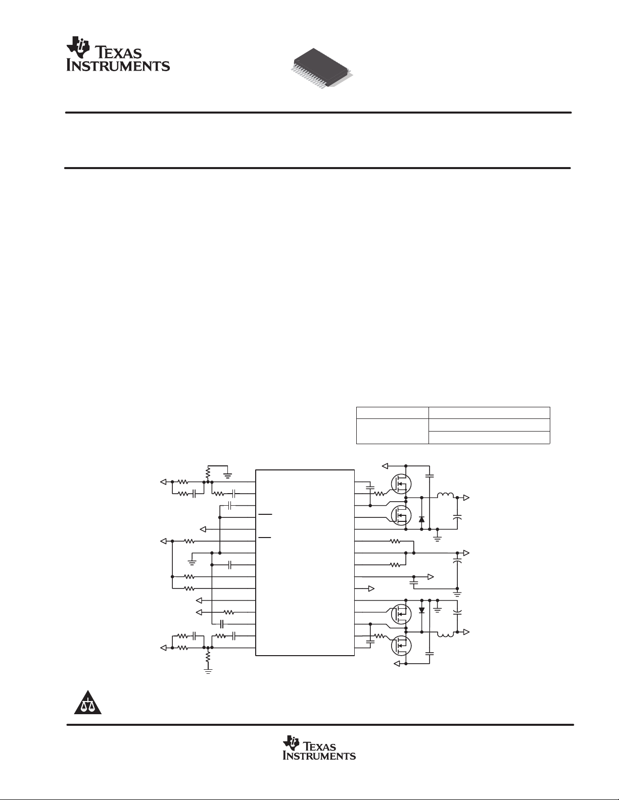
SIMPLIFIED
APPLICATION
DIAGRAM
VO1
VO2
VIN
VO1
VO2
VREG5
1
INV1
2
COMP1
3
SSTRT1
4
SKIP
5
VO1_VDDQ
6
DDR
7
GND
8
REF_X
9
ENBL1
10
ENBL2
11
VO2
12
PGOOD
13
SSTRT2
14
COMP2
15
INV2
TPS51020
DESCRIPTION
The TPS51020 is a multi-function dualsynchronous step-down controller for notebook
system power. The part is specifically designed
for high performance, high efficiency applications
where the loss associated with a current sense
resistor is unacceptable. The TPS51020 utilizes
feed forward voltage mode control to attain high
efficiency without sacrificing line response.
Efficiency at light load conditions can be
maintained high as well by incorporating autoskip
operation. A selectable, Suspend to RAM (STR)
supported, DDR option provides a one chip
solution for all switching applications from
5-V/3.3-V supply to a complete DDR termination
solution.
ORDERING INFORMATION
TA PLASTIC TSSOP (DBT)
VBST1
OUT1_U
LL1
OUT1_D
OUTGND1
TRIP1
VIN
TRIP2
VREG5
REG5_IN
OUTGND2
OUT2_D
LL2
OUT2_U
VBST2
−40°C to 85°C
VIN
30
29
28
27
26
25
24
23
22
21
EXT_5V
20
19
18
17
16
VIN
TPS51020DBTR (T&R)
VREG5
TPS51020DBT
VO1
VIN
VO2
UDG−03144
Please be aware that an important notice concerning availability, standard warranty, and use in critical applications of
Texas Instruments semiconductor products and disclaimers thereto appears at the end of this data sheet.
!"#$%&" ' ()##*& %' "! +),-(%&" .%&*/
#".)(&' ("!"#$ &" '+*(!(%&"' +*# &0* &*#$' "! *1%' '&#)$*&'
'&%.%#. 2%##%&3/ #".)(&" +#"(*''4 ."*' "& *(*''%#-3 (-).*
&*'&4 "! %-- +%#%$*&*#'/
www.ti.com
Copyright 2003, Texas Instruments Incorporated
1
Page 2
V
Ouput voltage range
V
I/O Voltage
SLUS564C − JULY 2003 − REVISED OCTOBER 2008
ABSOLUTE MAXIMUM RATINGS
Over operating free-air temperature range unless otherwise noted. All voltage values are with respect to the network ground terminal unless
otherwise noted.
Input voltage range
Ouput voltage range
Output current range
Operating free-air temperature range, T
Storage temperature range, T
Junction temperature range, T
Lead temperature 1,6 mm (1/16 inch) from case for 10 seconds 300
(1)
TPS51020 UNIT
VBST1, VBST2 −0.3 to 35
VBST1, VBST2 (wi th respect to LL ) −0.3 to 7
VIN, TRIP1, TRIP2, ENBL1, ENBL2, DDR −0.3 to 30
SKIP, INV1, INV2 −0.3 to 7
OUT1_U, OUT2_U −1 to 35
OUT1_U, OUT2_U (wi th respect to LL ) −0.3 to 7
LL1, LL2 −1 to 30
REF_X −0.3 to 15
PGOOD, VO1_VDDQ, VO2, OUT1_D, OUT2_D, COMP1, COMP2, VREG5,
SSTRT1, SSTRT2
OUTGND1, OUTGND2 −0.3 to 0.3
VREG5 70
REF_X 7
A
stg
J
−0.3 to 7
−40 to 85
−55 to 150
−40 to 125
V
mA
°C
RECOMMENDED OPERATING CONDITIONS
MIN TYP MAX UNIT
Supply voltage, VIN 4.5 28
Supply voltage, VBST1, VBST2 4.5 33
ENBL1, ENBL2, DDR, TRIP1, TRIP2 −0.1 28
OUT1_U, OUT2_U −0.8 33
OUT1_U, OUT2_U (wi th respect to LL ) −0.1 5.5
LL1, LL2 −0.8 28
I/O Voltage
Source current
Operating free-air temperature, T
(1)
Stresses beyond those listed under absolute maximum ratings may cause permanent damage to the device. These are stress ratings only,
and functional operation of the device at these or any other conditions beyond those indicated under ”recommended operating conditions” is
not implied. Exposure to Absolute Maximum Rated conditions for extended periods may affect device reliability
REF_X −0.1 12
SSTRT1, SSTRT2, COMP1, COMP2 −0.1 5.5
SKIP, INV1, INV2 −0.1 5.5
PGOOD VO1_VDDQ, VO2 −0.1 5.5
OUT1_D, OUT2_D, VREG5 −0.1 5.5
VREG5 60
REF_X 5
A
−40 85 °C
DISSIPATION RATING TABLE
PACKAGE
30-pin DBT 874 mW 7.0 mW/°C 454 mW
TA < 25°C
POWER RATING
FACTOR ABOVE TA = 25°C
DERATING
TA = 85°C
POWER RATING
V
mA
2
www.ti.com
Page 3
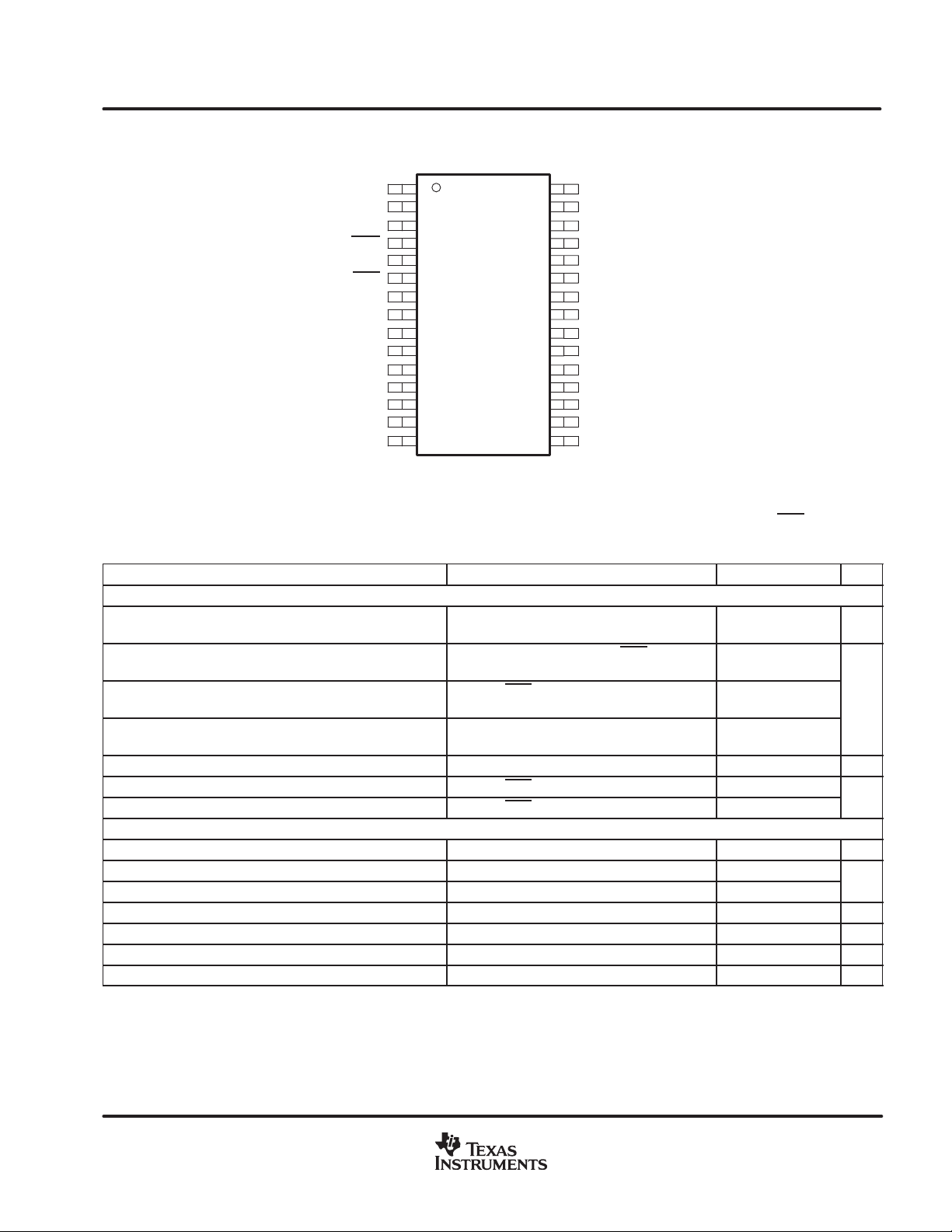
TSSOP (0.5 mm)
DBT PACKAGE
(TOP VIEW)
INV1
COMP1
SSTRT1
SKIP
VO1_VDDQ
DDR
GND
REF_X
ENBL1
ENBL2
VO2
PGOOD
SSTRT2
COMP2
INV2
1
2
3
4
5
6
7
8
9
10
11
12
13
14
15
30
29
28
27
26
25
24
23
22
21
20
19
18
17
16
VBST1
OUT1_U
LL1
OUT1_D
OUTGND1
TRIP1
VIN
TRIP2
VREG5
REG5_IN
OUTGND2
OUT2_D
LL2
OUT2_U
VBST2
ELECTRICAL CHARACTERISTICS
TA = −40°C to 85°C, 4.5 V < VIN < 20 V, C
INVx = COMPx, RSSTRTx = OPEN, TRIP1 = TRIP2 = VIN, LLx = GND, VBSTx = LLx+5, C
OUTGNDx = 0 V , VO1_VDDQ = VO2 = 0 V (unless otherwise stated)
PARAMETER
INPUT CURRENTS
I
VIN
I
VIN(STBY)VIN
I
VIN(SHDN)VIN
I
VIN(REG5)
I
REG5
I
VBSTx
I
VBSTx
VREG5 INTERNAL REGULATOR
V
VREG5
V
LD5
V
LN5
V
THL
V
HYS(UV)
V
TH(SW)
V
HYS(SW)
VIN supply current
standby current
shutdown current
VIN supply current, REG5_IN as 5-V input
current
REG5_IN input supply current REG5V_IN = 5 V, OSC = OFF 1.0 1.7 mA
VBST supply current ENBLx = DDR = VIN 0.05 1.00
VBST shutdown current ENBLx = DDR = 0 V 0.05 1.00
VREG5 voltage I
Load regulation 0 mA ≤ I
Line regulation I
UVLO threshold voltage High to low 3.45 3.65 3.85 V
UVLO hysteresis 100 200 300 mV
Switchover voltage REG_IN voltage 4.2 4.5 4.8 V
Switchover hysteresis 50 250 mV
= 0.1 µF, C
VIN
= 2.2 µF, C
VREG5
REG5V_IN = OPEN, TRIPx = VIN,
OSC = OFF
ENBLx = 0 V, DDR = VIN,
REG5V_IN = OPEN, OSC = OFF
ENBLx = DDR = 0 V,
REG5V_IN = OPEN
REG5V_IN = 5 V, OSC = OFF 200 500
= 0 A 4.8 5.0 5.2 V
OUT
OUT
= 20 mA, 7 V≤VIN ≤ 28 V 0.4% 2.0%
OUT
= 0.01 µF, PGOOD = 0.2 V, ENBLx = DDR = VIN,
REF_X
TEST CONDITIONS MIN TYP MAX UNIT
≤ 50 mA, VIN = 12 V 0.6% 2.5%
SLUS564C − JULY 2003 − REVISED OCTOBER 2008
(OUTx_U, OUTx_D)
=1 nF, REG5_IN = 0V, GND =
1.4 2.2 mA
350 550
0.05 1.00
µA
µA
www.ti.com
3
Page 4
)
)
SLUS564C − JULY 2003 − REVISED OCTOBER 2008
ELECTRICAL CHARACTERISTICS (continued)
TA = −40°C to 85°C, 4.5 V < VIN < 20 V, C
INVx = COMPx, RSSTRTx = OPEN, TRIP1 = TRIP2 = VIN, LLx = GND, VBSTx = LLx+5, C
OUTGNDx = 0 V , VO1_VDDQ = VO2 = 0 V (unless otherwise stated)
PARAMETER UNITMAXTYPMINTEST CONDITIONS
REF_X REFERENCE VOLTAGE
V
REF10
V
LD10
V
LN10
V
REFVTT
V
REFVTT
POWERGOOD COMPARATORS
V
THDUAL(PG
V
THDDR(PG
T
PG(del)
DIGITAL CONTROL INPUTS
V
IH
V
IL
I
INLEAK
VO1_VDDQ and VO2
R
VOUT
V
VOUTOK
V
VO2LEAK
R
VOUT
UNDERVOLTAGE AND OVERVOLTAGE PROTECTION
V
OVPDUAL
V
OVPDDR
T
OVP(del)
V
UVPDUAL
V
UVPDDR
T
UVP(del)
OVERCURRENT and INPUT VOLTAGE UVLO PROTECTION
I
TRIPSNK
I
TRIPSRC
TC
ITRIP
V
OCPHI
V
OCPLO
V
VINUVLO
V
VINHYS
10-V reference voltage VIN = 14 V, I
Load regulation 0 mA ≤ I
Line regulation I
VTT reference voltage
VTT reference load regulation 0 mA ≤ IO ≤ 3 mA 0.75%
PGOOD threshold (dual mode)
PGOOD threshold (DDR)
PGOOD delay time
High-level input voltage, logic DDR, ENBL1, ENBL2, SKIP 2.2
Low-level input voltage, logic DDR, ENBL1, ENBL2, SKIP 0.3
Logic input leakage current DDR, ENBL1, ENBL2, SKIP= 5 V |1.0| µA
VOx sink impedance V
VOx low restart voltage Fault condition removed, restart 0.25 0.32 0.40 V
VOx input leakage current DDR= VIN, VOx = 5 V |1.0| µA
VO1_VDDQ input impedance DDR= 0 1.5 MΩ
OVP trip output threshold (dual) Sensed at INVx 945 970 1010 mV
OVP trip output threshold (DDR) VO1_VDDQ = 2.5 V 1.31 1.36 1.41 V
OVP propagation delay time
UVP trip output threshold (dual) Sensed at INVx 510 553 595
UVP trip output threshold (DDR) VO1_VDDQ = 2.5 V 750 813 875
UVP propagation delay time 4096 clks
TRIPx sink current V
TRIPx source current V
TRIP current temperature coeficient
High-level OCP comparator offset voltage
Low-level OCP comparator offset voltage
VIN UVLO trip threshold REF5V_IN = 4.8 V 3.7 3.9 4.1 V
VIN UVLO trip hysteresis 100 200 300 mV
= 0.1 µF, C
VIN
(1)
(1)
= 2.2 µF, C
VREG5
OUT
= 100 µA, 14 V≤VIN ≤28 V 5%
OUT
DDR = 0 V wrt VO1_VDDQ input divided by 2
V
= 2.5 V
VO1
Undervoltage PGOOD 765 786 808
Overvoltage PGOOD
Undervoltage PGOOD,
VO1_VDDQ = 2.5 V
Overvoltage PGOOD,
VO1_VDDQ = 2.5 V
INVx > undervoltage PGOOD,
Delay time from SSTRTx > 1.5 V to PGOOD
going high
= 0.5 V, fault engaged 6 10 Ω
VOUTx
= VIN − 100 mV, TA = 25°C 11 13 15
TRIPx
= 100 mV, TA = 25°C 10 13 16
TRIPx
TA = 25°C 4200
(1)
(1)
= 0.01 µF, PGOOD = 0.2 V, ENBLx = DDR = VIN,
REF_X
≤ 2 mA, VIN = 18 V -12% -20%
(OUTx_U, OUTx_D)
= 0 A 8.5 10.0 11.0 V
OUT
=1 nF, REG5_IN = 0V, GND =
1.5%
892 920 945
1.12 1.14 1.16
1.28 1.31 1.33
2048 clks
20 µs
0 |3.0|
0 |5.0|
mV
V
V
mV
µA
ppm/
°C
mV
4
www.ti.com
Page 5
mV
MAX
DC
MAX
Maximum duty cycle
kHz
SLUS564C − JULY 2003 − REVISED OCTOBER 2008
ELECTRICAL CHARACTERISTICS (continued)
TA = −40°C to 85°C, 4.5 V < VIN < 20 V, C
INVx = COMPx, RSSTRTx = OPEN, TRIP1 = TRIP2 = VIN, LLx = GND, VBSTx = LLx+5, C
OUTGNDx = 0 V , VO1_VDDQ = VO2 = 0 V (unless otherwise stated)
PARAMETER UNITMAXTYPMINTEST CONDITIONS
0.85-V REFERENCE CONTROL LOOP
V
REFCH1
V
REFTC1
V
REFLN1
V
CHMM
CONTROL LOOP: SKIP HYSTERSTIC COMPARATOR AND ZERO CURRENT COMPARATOR
V
LLHYS
V
LLOFF
V
ZOFF
T
HLTOLL
T
HLTOHL
CONTROL LOOP ERROR AMPLIFIER
I
EASRC
I
EASNK
F
UGB
A
OL
CMR
COMP
I
INVLEAK
CONTROL LOOP: DUTY CYCLE, VOLTAGE RAMP, CHANNEL PHASE AND PWM DELAY PATH
DC
PH
CH
T
MIN
TIMERS: INTERNAL OSCILLATOR
f
OSC(hi)
f
OSC(lo)
f
OSC(tc)
(1)
Ensured by design. Not production tested.
(2)
Maximum 450-kHz frequency can be achieved when both channels are enabled.
(3)
270 kHz is the default frequency during start-up for both channels.
(4)
See Table 1.
(5)
See PWM detailed description
Error amplifier reference, channel 1 initial
accuracy
Error amplifier reference, channel 1
change with accuracy
Error amplifier reference, channel 1
change with line
Channel 2 to channel 1 voltage mismatch 0 |5.0| mV
Skip hysteresis comparator hysteresis
Lload hysteresis comparator offset
Zero current comparator offset
PWM skip delay time 8
Skip to PWM delay time 1
COMPx source current 0.2 0.9
COMPx sink current 0.2 0.7
Unity gain bandwidth
Open loop gain
COMPx voltage range
INVx input current |0.5| µA
Maximum duty cycle
Channel to channel phase difference
OUTX_U minimum pulse width
Fast oscillator frequency initial accuracy
Slow oscillator frequency initial accuracy R
Oscillator frequency over line and temperature Trimmed for 360 kHz 306 360 414
(1)
(1)
(4)
(1)(6)
= 0.1 µF, C
VIN
(1)
(1)
(1)
(5)
(1)
= 2.2 µF, C
VREG5
Measure COMP1, COMP1= INV1,
TA = 25°C
f
= 270 kHz
OSC
f
= 360 kHz
OSC
f
= 450 kHz
OSC
PWM phase reversal only 180 °
(2)
R
SSTRTx
SSTRTx
= OPEN 450
= 1MΩ or V
= 0.01 µF, PGOOD = 0.2 V, ENBLx = DDR = VIN,
REF_X
(3)
(2)
(OUTx_U, OUTx_D)
= 3 V 270
SSTRT
=1 nF, REG5_IN = 0V, GND =
0.84 0.85 0.86 V
0.5%
0.1%
1 2 3
0 1
10 18
2.5 MHz
80 dB
0.4 VREG5−3 V
86% 88%
84% 85%
80% 82%
100 ns
mV
clks
mA
kHz
www.ti.com
5
Page 6
SLUS564C − JULY 2003 − REVISED OCTOBER 2008
ELECTRICAL CHARACTERISTICS (continued)
TA = −40°C to 85°C, 4.5 V < VIN < 20 V, C
INVx = COMPx, RSSTRTx = OPEN, TRIP1 = TRIP2 = VIN, LLx = GND, VBSTx = LLX+5, C
OUTGNDx = 0 V, VO1_VDDQ = VO2 = 0 V (unless otherwise stated)
PARAMETER
TIMERS: SOFT-START RAMP GENERATOR
I
SSQ
I
SSDQ
V
REFTRK
V
SSOK
V
SSFIN
V
SSCLP
OUTPUTS: INTERNAL BST DIODE
V
FBST
I
RBST
OUTPUTS: N-CHANNEL MOSFET GATE DRIVERS
R
USRC
R
DSRC
R
USNK
R
DSNK
T
DEAD
(1)
Ensured by design. Not production tested.
(2)
Maximum 450-kHz frequency can be achieved only when both channels are enabled.
(3)
270 kHz is the default frequency during start-up for both channels.
(4)
See Table 1.
(5)
See PWM detailed description
(6)
Feedforward Gain can be approximated as follows:
V
RAMP
At the running duty cycle, the V
(7)
See waveform point A in Figure 1
(8)
See waveform point B in Figure 1
(9)
See waveform point C in Figure 1
SSTRTx charge current V
SSTRTx discharge current V
SSTRTx at SMPS regulation point voltage
SSTRTx OK to restart voltage 0.23 0.29 0.35
SSTRTx finished voltage
SSTRTx frequency select voltage
Forward voltage
Reverse current V
OUTx_U source impedance 3 10
OUTx_D source impedance 3 10
OUTx_U sink impedance 2.5 5.0
OUTx_D sink impedance 2.5 5.0
Gate non-overlap dead time 100 ns
= K1×VIN+B1, V
OFFSET
=K2×VIN×+B2 where K1=0.017, K2=0.01, B1=0.35 V, B2=0.4 V.
COMP
= 0.1 µF, C
VIN
(8)
(9)
should be approximately: V
VREG5
(7)
= 2.2 µF, C
SSTRTx
SSTRTx
(V
VREF5
TA = 25°C
RBST
= 0.01 µF, PGOOD = 0.2 V, ENBLx = DDR = VIN,
REF_X
TEST CONDITIONS MIN TYP MAX UNIT
= 1 V 1.8 2.3 2.9 µA
= 0.5 V 0.1 mA
− V
= 30 V 0.1 0.5 µA
COMP
VBSTx
+ V
OUT
), V
VREF5
ǒ
K1 )
(OUTx_U, OUTx_D)
= 5 V , IF = 10 mA
B1
Ǔ
(
)
VIN
K2 VIN ) B2
=1 nF, REG5_IN = 0V, GND =
1.00 1.22 1.45
1.4 1.5 1.6
3.35 3.60 3.80
0.80 0.85 V
)
V
Ω
Table 1. Frequency Selection
SSTRT1 SSTRT2 FREQUENCY (kHz)
C
1 MΩ || C
C
1 MΩ || C
(10)
Although selection is made by placing a 1M resistor in parallel with the SSTRTx timing
capacitor, the softstart time to 0.85V is altered by about only 20%.
6
only C
SSTRT
to GND C
SSTRT
only 1 MΩ || C
SSTRT
to GND 1 MΩ || C
SSTRT
only 450
SSTRT
only 360
SSTRT
SSTRT
SSTRT
www.ti.com
to GND 360
to GND 270
(10)
Page 7
I/O
DESCRIPTION
f
that channel attempts to turn on. If both ENBL1 and ENBL2 are low then the 10-V (or (VO1_VDDQ)/2 output)
ENBL1
ENBL2
5.0
3.6
1.5
1.2
0
5.0
− Soft-Start Voltage − V
3.6
SSTRT
V
1.5
1.2
0
fSW − Switching Frequency − kHz
270 360
t1t0 t3t2 t4 t5
470
360
SSTRT1
470 270
SSTRT2
t − Time
R
SSTRT1
= R
SSTRT2
= OPEN = 450 kHz
Figure 1
SLUS564C − JULY 2003 − REVISED OCTOBER 2008
ENBL1
ENBL2
fSW − Switching Frequency − kHz
5.0
C
B
A
C
B
A
3.6
1.5
1.2
0
5.0
− Soft-Start Voltage − V
3.6
SSTRT
V
1.5
1.2
0
270
t1t0 t3t2 t4 t5
360
270
SSTRT1
t − Time
R
SSTRT1
= 1 MΩ, R
SSTRT2
Figure 2
360
270
SSTRT2
= OPEN = 360 kHz
TERMINAL FUNCTIONS
TERMINAL
NAME NO.
COMP1 2 O
COMP2 14 O
DDR 6 I
ENBL1 9 I
ENBL2 10 I
GND 7 O Signal ground pin.
INV1 1 I
INV2 15 I
LL1 28 I/O
LL2 18 I/O
OUT1_D 27 O
OUT2_D 19 O
OUT1_U 29 O
OUT2_U 17 O
OUTGND1 26 O
OUTGND2 20 O
Error amplifier output. Connect feedback network to this pin and INVx for compensation of control loop.
DDR selection pin. If this pin is grounded, the device runs in DDR Mode. The error amplifier reference for VO2
is (VO1_VDDQ)/2, the REF_X output voltage becomes (VO1_VDDQ)/2 and skip mode is disabled for VO2,
Also, VREG5 is turned off when both ENBLx are at low in this mode. If this pin is at 2.2-V or higher, the device
runs in ordinary dual SMPS mode (dual mode), then the error amplifier reference for VO2 is connected to internal 0.85-V reference, the REF_X output voltage becomes 10 V, VREG5 is kept on regardless of ENBLx status.
CAUTION: Do not toggle DDR
TTL Enable Input. If ENBLx is greater than 2.2 V, then the VREG5 is enabled (DDR mode) and the SMPS o
voltage as well as the oscillator are turned off. (See Table 2)
Error amplifier inverting input. Also input for skip comparator, and OVP/UVP comparators.
Switch-node connection for high-side driver and overcurrent protection circuitry.
Synchronous N-channel MOSFET driver output.
High-side N-channel MOSFET driver output.
Ground return for OUTx_D.
while ENBL1 or ENBL2 are high. (See Table 2)
www.ti.com
7
Page 8
I/O
DESCRIPTION
t
time. A constant current fed to this capacitor ramps the reference during startup. Frequency selection is de-
time. A constant current fed to this capacitor ramps the reference during startup. Frequency selection is de-
the channel can start-up again. If DDR is low, then the VO1_VDDQ pin must be connected to the VDDQ output
-
SLUS564C − JULY 2003 − REVISED OCTOBER 2008
TERMINAL FUNCTIONS (continued)
TERMINAL
NAME NO.
Power good output. This is an open drain pull-down pin for power good. It remains low during soft-start until
PGOOD 12 O
REF_X 8 O
REG5_IN 21 I
SSTRT1 3 I
SSTRT2 13 I
SKIP 4 I
TRIP1 25 I
TRIP2 23 I
VBST1 30 I
VBST2 16 I
VO1_VDDQ 5 I
VO2
VREG5 22 O Internal, 60-mA, 5-V regulator output. DDR, ENBL1 or ENBL2 high ( > 2.2V) turns on the 5 V regulator.
VIN 24 I
11 I
both outputs become within ±7.5%. If INV1 or INV2 is out of regulation, or VREG5V goes under UVLO then this
pin goes low. The internal delay timer counts 2048 clks at low to high (by design, no delay for high to low). If
ENBLx is low, and the power good output is high, then the power good signal for that channel is ignored.
10-V N-channel MOSFET bias or (VO1_VDDQ)/2 reference output. If dual mode is selected (DDR > 2.2 V)
then this pin provides a low 10-V current (< 2 mA) bias, dropped down from VIN, for the SO – S5 switched
N-channel MOSFETs. If DDR mode is selected (DDR
of 3 mA source current. This bias/reference is shut off when ENBL1 and ENBL2 are both low. (See Table 2)
External 5V regulator Input. If this pin is above 4.7 V, then the 5 V circuit bias switches from the VREF5 to the
supply presented to REG5_IN.
Soft-start/frequency select input. Connect a capacitor between SSTRTx and ground for adjusting the softstar
scribed in Table 1. The soft-start capacitor is discharged upon UVLO/OVP/UVP, or when ENBLx is asserted
low.
Skip mode selection pin. Ground for automatic control between PWM mode in heavy load and hysteretic operation in light load. Tie high for PWM only operation for the entire load condition. If DDR
mode is disabled for Channel 2.
Channel 1 overcurrent trip point voltage input. Connect a resistor between TRIP1 and the high-side N-channel
MOSFET input conversion voltage for high-side N-channel MOSFET UVP current limit shut down. Connect
resistor between TRIP1 and GND for low-side N-channel MOSFET overcurrent latch shutdown.
Channel 2 overcurrent trip point voltage input. Connect a resistor between TRIP2 and the high-side N-channel
MOSFET input conversion voltage for high-side N-channel MOSFET UVP current limit shut down with a 180°
channel phase shift. Connect resistor between TRIP2 and GND for low-side N-channel MOSFET over current
latch shut-down. The oscillator voltage ramp adjustment (the feed-forward feature) for channel 2 is disabled
when this pin is tied to ground via a resistor.
Supply Input for high-side N-channel FET driver. Typically connected via charge pump from LLx.
Output discharge pin. Connect this pin to the SMPS output. The output is discharged to at least 0.3 V before
since this pin works as the VDDQ feedback to generate the VTT reference voltage and VO2 should be con
nected to GND since VTT must remain in a high-impedance state during S3 mode.
High-voltage input. Typically the battery voltage. This pin serves as inputs for the VREF5 regulator, the REF_X
regulator and positive input for overcurrent comparators. Precaution should be taken for tracing between this
pin and the high-side N-channel MOSFET drain where positive node of TRIPx resistors are located.
= GND) then this pin becomes (VO1_VDDQ)/2 capable
is grounded, then skip
Table 2. Reference Regulator Control
MODE DDR ENBL1 ENBL2 VREF5 REF_X OSC
DDR LOW LOW LOW OFF OFF OFF
DDR LOW LOW HIGH ON
DDR LOW HIGH LOW ON
DDR LOW HIGH HIGH ON
DUAL HIGH LOW LOW ON OFF OFF
DUAL HIGH LOW HIGH ON 10 V ON
DUAL HIGH HIGH LOW ON 10 V ON
DUAL HIGH HIGH HIGH ON 10 V ON
8
www.ti.com
OFF
VO1_DDR
2
VO1_DDR
2
ON
ON
ON
Page 9
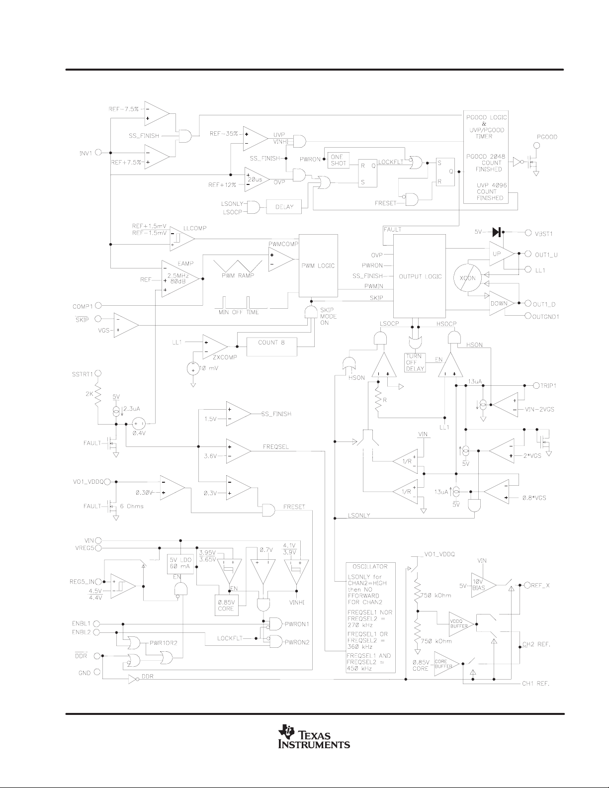
FUNCTIONAL BLOCK DIAGRAM
SLUS564C − JULY 2003 − REVISED OCTOBER 2008
Shows Channel 1 (VO1_VDDQ) and the supporting circuitry.
www.ti.com
9
Page 10

SLUS564C − JULY 2003 − REVISED OCTOBER 2008
APPLICATION INFORMATION
PWM OPERATION
The PWM control block utilizes a fixed-frequency, feed-forward, voltage-mode control scheme with a
wide-bandwidth, low-impedance output error amplifier as the voltage servo control block. This scheme allows
the highest efficiency down conversion while maintaining excellent line regulation and fast transient response.
Loop compensation is programmed by connecting a filter network between the COMPx pin and the INVx pin.
The wide bandwidth error amplifier handles conventional Type II compensation or Type III compensation when
using ceramic capacitors for the converter output. For channel one, the reference signal for the control loop is
always a precision 0.85-V internal reference, while the channel two loop reference is either the 0.85-V reference
or, in the case of DDR
amplifier appears at the COMPx pin and is compared to a buffered version of the 0.6-V oscillator ramp. When
TRIP2 pin is tied to VIN through a resistor, the voltage ramp is further modulated by the input voltage, VIN, to
maintain a constant modulator gain. If the TRIP2 pin is connected to ground through a resistor , then the voltage
ramp remains fixed regardless of VIN value.
The oscillator frequency is internally fixed and can be selected at 270 kHz, 360 kHz or 470 kHz by insertion of
a clamping resistor on the SSTRTx pin per Table 1. For example, 470 kHz can be attained when both SSTR Tx
voltages exceed 3.5 V, as described in WAVEFORM1. The controller begins with 270 kHz in the first stage of
the softstart, and then increases to 470 kHz at the steady state. When 270 kHz is selected, both of SSTRTx
voltages are kept below 3.5 V so that the frequency is the same 270 kHz for the entire operation.
mode, one half the VO1_VDDQ voltage, (VO1_VDDQ)/2. The output signal of the error
Two channels are operated in 180 degrees out-of-phase interleave switching mode. This interleaving helps
reduce the input current ripple requirement for the input capacitor . However, because the PWM loop determines
both the turn-off AND turn-on of the high-side MOSFET, this 180 degree operation may not be apparent by
looking at the LLx nodes only. Rather , the turn-of f cycle of one channel always corresponds to the turn-on cycle
of the other channel and vise-versa. As a result, input ripple is reduced and dynamic response is improved over
a broad input voltage range.
MAXIMUM DUTY CYCLE
Because most notebook applications typically run from three to four cell Li−Ion or run from a 20-V adapter , 100%
duty cycle operation is not required. Rather, the TPS51020 is optimized for low duty ratio step-down conversion.
As a result of limiting the duty cycle, the flying BST capacitor is refreshed reliably and the low-side over current
detection circuitry is capable of detecting an overcurrent condition even if the output is stuck between the
regulation point and UVP. The maximum duty cycle for each operating frequency is 88% for 270 kHz, 85% for
360 kHz and 82% for 470 kHz.
It should be noted that if the system is operating close to maximum (or minimum) duty cycle, it may be difficult
for the converter to respond quickly during line/load transients or state changes (such as frequency switching
during soft start or PWM to SKIP mode transitions). This slow response is due to the dynamic range of the COMP
pin and is usually not a result of poor phase compensation. In the case of minimum duty cycle operation, the
slow response is due to the minimum pulse width of the converter (100 ns TYP). In this case (counter intuitively),
it may be advisable to slow down the switching frequency of the converter in order to improve response time.
10
www.ti.com
Page 11

SLUS564C − JULY 2003 − REVISED OCTOBER 2008
APPLICATION INFORMATION
SKIP MODE OPERATION
If the SKIP pin is set HIGH, the SMPS operates in the fixed PWM mode. While a LOW signal is applied, the
controller operates in autoskip mode. In the autoskip mode, the operation changes from constant frequency
PWM mode to an energy-saving skip mode automatically by detecting the edge of discontinuous current mode.
During the skip mode, the hysteretic comparator monitors output voltage to trigger high side on at the next
coming oscillator pulse after the lower level is detected. Several sequential pulses may be seen, especially in
the intermediate load level, before output capacitor is charged up to the higher level and waits for next cycle.
In the skip mode, frequency varies with load current and input voltage.
Skip mode for SMPS_2 is disabled regardless of the SKIP
and DDR Mode section). This is because current sink capability is required for V
needs to be kept on when the inductor current flows inversely. SMPS_1 is still capable of skip mode operation
while DDR Mode.
pin status if DDR mode is selected (see Dual Mode
, so that rectifying MOSFET
TT
CASCADE CONFIGURATION
If the TRIP2 pin is tied through a resistor to the input voltage, the TPS51020 assumes that the conversion voltage
for channel two is the VIN voltage, usually VBATT. Conversely, i f TRIP2 is tied through a resistor to ground, the
controller assumes that the conversion voltage for channel two is the output voltage of channel one or some
other stable bus voltage.
DUAL MODE AND DDR MODE
TPS51020 provides one-chip solution for system power supply, such as for 5 V, 3.3 V or 1.8 V, and a dual
switcher DDR power supply. By simply selecting DDR
the instructions below, TPS51020 gives a complete function set required for the DDR termination supply such
as VDDQ/2 tracking V
is set high ( > 2.2 V), the TPS51020 runs in dual mode, that is, each converter produces an independent
If DDR
output voltage with respect to the internal 0.85-V reference. Bypass REF_X to ground by 0.01-µF. The
VO1_VDDQ or VO2 terminal should be connected to their corresponding switcher output. The 10-V reference
output can be used as FET switch biasing for power control during sleep states (see Figure 5). During this dual
mode, selection of autoskip mode or PWM mode made by SKIP
is set low ( < 0.3V), the TPS51020 operates as a dual switcher DDR supply; VDDQ from SMPS_1 and
If DDR
V
from SMPS_2 (DDR Mode). In this mode, the reference voltage for SMPS_2 is switched to (VO1_VDDQ)/2
TT
to track exactly half the voltage of SMPS_1, divided by internal resistors. VO1_VDDQ should be connected to
SMPS_1 output terminal to accomplish this. REF_X outputs the (VO1_VDDQ)/2 voltage after a buffer (5-mA
max). SKIP
from the output. Power source of SMPS_2 can either be the battery voltage (independent configuration), or the
VDDQ (cascade configuration) by user’s preference. When using the independent configuration, TRIP2 needs
to be connected to the VIN node via trip resistor. In case of cascade configuration, tie TRIP2 to GND via trip
resistor (see Figure 7).
controls only SMPS_1 and SMPS_2 is forced to operate in PWM mode so that current can be sink
CAUTION:Do NOT toggle DDR HIGH while ENBL1 or ENBL2 is high (see Table 2). REF_X
output switches to high voltage (10 V) and be applied to V
source/sink capability and VTT reference output.
TT
signal and some external configuration change following
applies to both SMPS_1 and SMPS_2.
directly
TTREF
www.ti.com
11
Page 12

SLUS564C − JULY 2003 − REVISED OCTOBER 2008
APPLICATION INFORMATION
5-V LINEAR REGULATOR (VREG5)
The VREG5 voltage is the bias for all the low voltage circuitry in the TPS51020 as well as the DC boost voltage
for the MOSFET gate drivers. Total available current is 60 mA. Bypass this pin to GND by 4.7-µF. The under
voltage lockout (UVLO) circuit monitors the output of this regulator to protect internal circuitry from low input
voltages. If 5 V i s applied to REG5_IN from either the SMPS output or an alternate 5 V, then the linear regulator
is turned off and the VREG5 pin is switched over to REG_IN. This operation enhances the efficiency of the
overall power supply system because the bulk of the quiescent current now runs from the 5-V output instead
of VIN (VBAT). In this configuration, ensure that VREG5_IN is less than or equal to V
EXTERNAL 5V INPUT (REG5_IN)
When a 5-V bus is available, VIN does not need to be connected to the battery. In this configuration, VIN should
be connected to REG5_IN.
LOW-SIDE N-CHANNEL FET DRIVER
VIN
.
The low-side driver is designed to drive high current low R
voltage is 5.5 V. The drive capability is represented by its internal resistance, which are 3 Ω for VREG5 to
OUTx_D and 2.5 Ω for OUTx_D to OUTGNDx. A dead time is internally generated between top MOSFET off
to bottom MOSFET on, and bottom MOSFET off to top MOSFET on, in order to prevent shoot through.
The low-side driver is typically turned off during all fault modes except for OVP. When an OVP condition exists,
the low-side driver of the offending channel turns on and attempts to blow the protection fuse of the input supply.
N-channel MOSFET(s). The maximum drive
DS(on)
HIGH-SIDE N-CHANNEL FET DRIVER
The high-side driver is designed to drive high current, low R
a floating driver, a 5-V bias voltage is delivered from VREG5 supply. The instantaneous drive current is supplied
by the flying capacitor between VBSTx and LLx pins, 0.1-µF ceramic for typical applications. The boost diodes
are integrated and are sufficient for enhancing the high-side MOSFET. However, external boost diodes can also
be added from VREG5 to each VBSTx in case higher gate-to-source votlage is required.
The drive capability is represented by its internal resistance, which are as follows: 3 Ω for VBST to OUTx_U
and 2.5 Ω for OUTx_U to LLx. The maximum voltage that can be applied between OUTx_U pin and OUTGNDx
pin is 35 V.
N-channel MOSFET(s). When configured as
DS(on)
12
www.ti.com
Page 13

SLUS564C − JULY 2003 − REVISED OCTOBER 2008
APPLICATION INFORMATION
ENABLE AND SOFT-START
Each SMPS is switched into standby mode separately by grounding the corresponding ENBLx pin. The 5-V
supply is enabled if either the DDR
Softstart of each SMPS is achieved by slowly ramping the error amplifier reference voltage by following a
buffered version of the SSTRTx pin voltage. Designers can achieve their own start-up sequencing by simply
provide external timing signals since the startup times do not depend on the load current. The softstart time is
programmable by external capacitor connected from SSTRTx pin to the ground. Each SSTRTx pin sources
constant current, typically 2.3 µA. The output voltage of the SMPS ramps up from 0 V to its target regulation
voltage as the SSTRTx pin voltage increases from 0 V to 1.2 V. This gives the softstart time formula to be,
T
C
The soft-start capacitor is discharged upon UVLO, OVP or UVP is detected as well as ENBLx is set low.
SSTRT
(Farads) +
SSTRT
, ENBL1 or ENBL2 pin(s) goes high ( >2.2 V).
(sec) 2.3 10
1.2
*6
OUTPUT DISCHARGE (SOFT-STOP)
When an SMPS is turned off by ENBLx asserted low or the part enters a fault mode, both top and bottom drivers
are turned off. This may leave the output in a high impedance state that allows the voltage to persist for some
time. Output voltage should be discharged prior to the next power up. To achieve this, connect the output to the
VO1_VDDQ or VO2 pins.
These pins turn on a 6-Ω resistor to ground during an off or fault condition. Both the VO1_VDDQ and VO2 pin
must be discharged to 0.3 V before the TPS51020 restarts. The TPS51020 has the flexibility of adding a resistor
in series with the VOx pin and the output voltage in order to reduce the discharge current and reduce the total
power dissipation within the device. It should be noted that when this resistor is added the discharged voltage
threshold changes according to the following equation:
where
D R
D R
V
DISCHARGE
EXTERNAL
= 6 Ω
DS(on)
ǒ
R
EXTERNAL
+
is the series resistor between VOx and the output
R
DS(on)
) R
DS(on)
Ǔ
0.3
www.ti.com
13
Page 14

SLUS564C − JULY 2003 − REVISED OCTOBER 2008
APPLICATION INFORMATION
10-V N-CHANNEL FET BIAS or (VOUT1)/2 VTT VOLTAGE REFERENCE (REF_X)
TPS51020’s REF_X provides two functions depending on the operational mode. One is a linear regulator that
supply 10-V for FET switch biasing in the dual mode, the other is V
is high ( > 2.2 V) then the REF_X output is a convenient 10-V, 2-mA (maximum) output, useful for biasing
If DDR
N-channel FET switches typically used to manage S0, S3 and S5 sleep states where the main supply is switched
to many outputs. When V
is low, then the REF_X output becomes the VDDQ/2 (VO1_VDDQ/2) reference. This output is capable
If DDR
of 5-mA source current and is left on even if channel two (V
is < 12 V, REF_X approximately tracks VIN−2 V.
IN
switcher) is turned off. REF_X is turned off if ENBL1
TT
and ENBL2 are both low (see Table 2).
POWERGOOD
The TPS51020 has advanced powergood logic that allows single powergood circuit to monitor both SMPS
output voltages (see Figure 3 ).
reference voltage in the DDR mode.
TT
VOUT1
VOUT2
PGOOD Delay Counter
PGOOD
ENBL1
ENBL2
2048 c
2048 c
Resets Delay Counter
t0 t1 t2
Figure 3. PowerGood Timing Diagram
The PGOOD terminal is an open drain output. The PGOOD pin remains low until both power supplies have
started and have been in regulation ( ±7.5%) for 2048 clock pulses.
14
www.ti.com
Page 15

SLUS564C − JULY 2003 − REVISED OCTOBER 2008
APPLICATION INFORMATION
If one channel is enabled in the period between T0 and T1, (the other channel’s ramp time plus delay time,) the
PGOOD delay counter restarts counting softstart finish after the last channel has finished softstart. Enabling
after T1 is ignored by PGOOD until the channel finishes its softstart. If either of the SMPS output goes out by
± 7.5% or UVLO is detected while ENBLx is high, PGOOD pulls low. If a channel is disabled while the other is
still active PGOOD maintains it’s logic state and only monitor the active channel.
PROTECTION FUNCTIONS
The TPS51020 is equipped with input undervoltage lock out (UVLO), output undervoltage protection (UVP) and
overvoltage (OVP) protection. Overcurrent is detected using R
protected by triggering UVP, or latch off in some cases. The states of output drive signal depends on which
protection was involved. Please refer to each protection description below for the detail.
When the input voltage UVLO is tripped, the TPS51020 resets and waits for the voltage to rise up over the
threshold voltage and restart the device. Alternatively , if output UVP or OVP is triggered, the device latches off
after a delay time defined by the internal fault counter counting the PWM oscillator pulses. The VREF5 and
REF_X is kept on in this latch off condition. The fault latch can be reset by toggling both of ENBLx pins in DDR
mode. The fault latch can be reset by either toggling VIN or bringing DDR
to bring DDR
If a false trip of the UVLO appears due to input voltage sag during turn-on of the high-side MOSFET such as
a large load transient, first consider adding several micro-farads of input capacitance close to the MOSFET’s
drain. Also consider adding a small V
should be connected to the same node as VIN pin of the device when this filter is applied. The filter resistor
should be as small as possible since a voltage drop across this resistor biases the OCP trip point.
high prior to ENBLx when TPS51020 is being used in dual mode.
filter, ex. a 2.2-Ω resistor and a 2.2-µF, for decoupling. The trip resistors
IN
of the external power MOSFETs and
DS(on)
, ENBL1 and ENBL2 all low. Be sure
UNDERVOLTAGE LOCKOUT PROTECTION
There are two undervoltage lock out protections (UVLO) in TPS51020. One is for VIN, which has a typical trip
threshold voltage 3.9 V and trip hysteresis 200 mV. The other is for VREF5, which has a typical trip threshold
voltage 3.65 V and trip hysteresis 300 mV. If either is triggered, the device resets and waits for the voltage to
rise up over the threshold voltage and restart the part. Please note this protection function DOES NOT trigger
the fault counter to latch off the part.
OVERVOLTAGE PROTECTION
For overvoltage protection (OVP), the TPS51020 monitors INVx voltage. When the INVx voltage is higher than
0.95V (+12%), the OVP comparator output goes high (after a 20-µs delay) and the circuit latches the top
MOSFET driver OFF, and bottom driver ON for the SMPS detected overvoltage. In addition, the output
discharge (softstop) function is enabled to discharge the output capacitor. The fault latch can be reset by either
toggling VIN or bringing DDR
TPS51020 is being used in dual mode.
, ENBL1 and ENBL2 all low. Be sure to bring DDR high prior to ENBLx when
UNDERVOLTAGE PROTECTION
For undervoltage protection (UVP), the TPS51020 monitors INVx voltage. When the INVx voltage is lower than
0.55 V (−35 %), the UVP comparator output goes high, and the internal FLT timer starts to count PWM oscillator
pulses. After 4096 clock pulses, the part latches off. Both top and bottom drivers are turned off at this condition.
Output discharge (soft-stop) function is enabled to discharge the output capacitor. The fault latch can be reset
by either toggling VIN or bringing DDR
when TPS51020 is being used in dual mode.
, ENBL1 and ENBL2 all low. Be sure to bring DDR high prior to ENBLx
www.ti.com
15
Page 16

SLUS564C − JULY 2003 − REVISED OCTOBER 2008
APPLICATION INFORMATION
OVERCURRENT PROTECTION
Overcurrent protection (OCP) is achieved by comparing the drain to source voltage of the high-side and low-side
MOSFET to a set point voltage. This voltage appears at the TRIPx pin and is defined by the conversion voltage,
typically VIN, minus the I × R drop of the I
conversion voltage. The offset of the internal comparators also plays a role in determining the overall accuracy
and set point of the OCP limit.
When the drain-to-source voltage of the synchronous MOSFET exceeds the set point voltage created by the
I × R drop (usually 20 mV to around 150 mV), the synchronous MOSFET on-time is extended into the next pulse
and the high-side MOSFET OCP comparator is enabled. If during the subsequent high-side on-time the
drain-to-source voltage of the high-side MOSFET exceeds the set point voltage, then the high-side on-time
pulse is terminated. This low-side extension/high-side termination action has the effect of decreasing the output
voltage until the UVP circuit is activated to turn off both the high-side and low-side drivers. The TPS51020 I
current has a temperature coefficient of 4200 PPM/°C.
current flowing through the external resistor connected to the
TRIP
TRIP
The threshold voltage for the OCP comparator is set by I × R drop across the trip resistor. The I
12.5-µA (typ) at R.T. so that the OCP point is given by following formula,
I
)
*6
RIPPLE
2
Ǔ
R
DS(on)
R
+
TRIP
Precaution should be taken with board layout in order to design OCP point as desired. The conversion voltage
point must avoid high current path. Any voltage difference between the conversion point and VIN input for the
TPS51020 is included in the threshold voltage. VIN plane layout should consider the other channels
high-current path as well.
A brief discussion is required for TRIP2 function. When TRIP2 is connected, via a resistor to GND, only low-side
OCP is used. This is the case for cascade configuration been selected. In this mode, UVP does not play a roll
in the shut off action and there is only a short delay between the over current trigger level been hit and the power
MOSFETs turn off. However, as with UVP, the SSTRTx pins are discharged and both SMPS goes though a
restart.
ǒ
I
OCP
12.5 10
TRIP
LAYOUT CONSIDERATIONS
Below are some points to consider before the layout of the TPS51020 design begins.
D Signal GND and power GND should be isolated as much as possible, with a single point connection
between them.
D All sensitive analog components such as INV, SSTRT, SKIP, DDR, GND, REF_X, ENBL and PGOOD
should be reference to signal GND and be as short as possible.
current is
D The source of low-side MOSFET, the Schottky diode anode, the output capacitor and OUTGND should be
referenced to power GND and be as short and wide as possible, otherwise signal GND is subject to the noise
of the outputs.
D PCB trace defined as the node of LL should be as short and wide as possible.
D Connections from the drivers to the gate of the power MOSFET should be as short and wide as possible
to reduce stray inductance and the noise at the LL node.
D The drain of high-side MOSFET, the input capacitor and the trip resistor should be as short and wide as
16
possible. For noise reduction, a 22-pF capacitor C
www.ti.com
can be placed in parallel with the trip resistor.
TRIP
Page 17

SLUS564C − JULY 2003 − REVISED OCTOBER 2008
APPLICATION INFORMATION
D The output voltage sensing trace and the feedback components should be as short as possible and be
isolated from the power components and traces.
D The low pass filter for VIN should be placed close to the TPS51020 and be referenced to signal GND.
D The bootstrap capacitor C
D VREG5 requires at least 4.7-µF bypass capacitor which should be placed close to the TPS51020 and be
referenced to signal GND.
D The discharge (VO1_VDDQ, VO2) should better have a dedicated trace to the output capacitor. In case of
limiting the discharge current, series resistors should be added.
D Ideally, all of the area directly under the TPS51020 chip should also be signal GND.
1
INV1
2
COMP1
3
SSTRT1
4
SKIP
5
VO1_VDDQ
6
DDR
7
Signal GND
GND
8
REF_X
9
ENBL1
10
ENBL2
11
VO2
12 19OUT2_DPGOOD
13
SSTRT2
14
COMP2
15
INV2
(connected from VBST to LL) should be placed close to the TPS51020.
BST
TPS51020
VBST1
OUT1_U
LL1
OUT1_D
OUTGND1
TRIP1
VIN
TRIP2
VREG5
REG5_IN
OUTGND2
LL2
OUT2_U
VBST2
30
C
Cvreg5
C
BST2
BST1
Rvin
Cvinbp
29
28
27
26
25
24
23
22
21
20
18
17
16
Cin1
L_FET1
L_FET2
Cin2
H_FET1
Cin
H_FET2
L01
Power GND
L02
Co1
Co2
Rtrip1 Ctrip1
Rtrips Ctrip2
CH1 Output Voltage (+)
+
CH1 Output Voltage (GND)
−
Input Voltage (+)
+
Input Voltage (GND)
−
CH2 Output Voltage (GND)
−
CH2 Output Voltage (+)
+
Figure 4. PCB Trace Guideline
www.ti.com
17
Page 18

25
−H
SLUS564C − JULY 2003 − REVISED OCTOBER 2008
APPLICATION INFORMATION
R102
100k
GND
R101
C12
R101
100k
6800p
R01
R02
100k
C22
C01a : Sanyo 35SVPD22M
C01c, C02, C03, C27 : Taiyo Yuden GMK325BJ225MH−B
C04a, C05a : Panasonic EEFUE0J151R
Q01, Q03 : Fairchild FDS6612A
Q02, Q04 : Fairchild FDS6690S
L01, L02 : Sumida CEP125−4R0MC−H
C14
3900p
49.7k
330
R03
10k
C15
0.01u
C19
0.01u
R09
10k
330
2200p
C20
3300p
R11
28.8k
R10
Figure 5. Typical Application Circuit: Dual (5V/6A + 3.3V/6A) from VBAT
R04
1.8k
(10V_REF)
R08
C01a
22u
R202
R200
GND
Q10
Q11
51k
Q12
GND
51k
Q15
R201
GND
Q13
Q14
R203
GND
Q01
R12
C08
1
TPS51020
INV1
2
COMP1
3
SSTRT1
4
SKIP
5
VO1_VDDQ
6
DDR
7
GND
8
REF_X
9
ENBL1
10
ENBL2
11
VO2
12
PGOOD
13
SSTRT2
14
COMP2
15
INV2
2.7k
OUTGND1
OUTGND2
R07
OUT1_U
OUT1_D
REG5_IN
OUT2_D
OUT2_U
VBST1
TRIP1
TRIP2
VREG5
VBST2
LL1
LL2
100k
0.1u
30
29
28
27
26
25
24
VIN
C11
R14
23
22
21
20
19
18
17
16
0.1u
R15
C02
2.2ux2
15
Q02
R13
18k
18k
15
R16
C27
0
C01c
0
Q04
C03
2.2ux2
Q03
L01
4u
C04a
C04c
0.01u
150u
GND
2.2u
C13
4.7u
GND
C05c
C05a
L02
4u
150u
0.01u
VBAT
8 V to 20 V
5V_OUT
5V_X
51k
3.3V_OUT
3.3V_X
51k
R102
GND
100k
R101
100k
C12
4700p
R01
C14
R02
7.62k
1.2k
R03
3.9k
C15
C19
R10
R11
1.2k
C22
2200p
4700p
0.01u
(VO1_VDDQ/2_REF)
0.01u
C20
6800p
19.7k
R04
4.7k
1
TPS51020
INV1
2
COMP1
3
SSTRT1
4
SKIP
5
VO1_VDDQ
6
DDR
7
GND
8
REF_X
9
ENBL1
10
ENBL2
11
VO2
12
PGOOD
13
SSTRT2
14
COMP2
15
INV2
R08
3.9k
OUTGND1
OUTGND2
R07
VBST1
OUT1_U
OUT1_D
TRIP1
TRIP2
VREG5
REG5_IN
OUT2_D
OUT2_U
VBST2
LL1
VIN
LL2
C11
100k
R12
15
C08
0.1u
30
29
28
27
26
25
24
23
22
21
20
19
18
17
16
0.1u
R14
(EXT_5V)
R15
R13
18k
18k
15
C02
2.2ux2
C27 C01c
C03
2.2ux2
Q03
Q01
Q02
R16
0
0 2.2u
Q04
GND
L01
5.6u
C04b
C04a
150u
C13
4.7u
C05b
C05a
150u
L02
5.6u
Figure 6. Typical Application Circuit: DDR(2.5V/6A + 1.25V/6A) from VBAT
C01a
22u
GND
C04c
0.01u
150u
GND
GND
C05c
150u
0.01u
C01a : Sanyo 35SVPD22M
C01c, C02, C03, C27 : Taiyo Yuden GMK325BJ2
C04a, C05a, C04b, C05b : Panasonic EEFUE0J151R
Q01, Q03 : Fairchild FDS6612A
Q02, Q04 : Fairchild FDS6690S
L01, L02 : Sumida CEP125−5R6MC
VBAT
8 V to 20 V
2.5V_OUT
1.25V_OUT
18
www.ti.com
Page 19

R102
GND
100k
R101
100k
SLUS564C − JULY 2003 − REVISED OCTOBER 2008
APPLICATION INFORMATION
VBAT
C01a
C05c
GND
0.01u
GND
0.01u
C12
4700p
R01
R02
7.62k
1.2k
R03
3.9k
C15
C19
R10
R11
1.2k
19.7k
C22
2200p
R04
C14
4.7k
4700p
0.01u
(VO1_VDDQ/2_REF)
0.01u
C20
R08
6800p
1
TPS51020
INV1
2
COMP1
3
SSTRT1
4
SKIP
5
VO1_VDDQ
6
DDR
7
GND
8
REF_X
9
ENBL1
10
ENBL2
11
VO2
12
PGOOD
13
SSTRT2
14
COMP2
15
INV2
3.9k
R07
VBST1
OUT1_U
LL1
OUT1_D
OUTGND1
TRIP1
VIN
TRIP2
VREG5
REG5_IN
OUTGND2
OUT2_D
LL2
OUT2_U
VBST2
100k
C11
R12
15
C08
0.1u
30
29
28
27
26
25
24
23
22
21
(EXT_5V)
20
19
18
17
16
0.1u
R15
R13
R14
C04d
15
2.5V_OUT
C02
GND
Q01
2.2ux2
Q02
18k
150u
R16
0
0
Q04
Q03
18k
L01
5.6u
C04b
C05a
C04c
150u
150u
GND
4.7u
C05b
150u
150u
C04a
C01cC27
2.2u
C13
GND
L02
5.6u
8 V to 20 V
22u
2.5V_OUT
1.25V_OUT
C01a : Sanyo 35SVPD22M
C01c, C02, C27 : Taiyo Yuden GMK325BJ225MH−B
C04a, C05a, C04b, C05b,C04d : Panasonic EEFUE0J151R
Q01, Q03 : Fairchild FDS6612A
Q02, Q04 : Fairchild FDS6690S
L01, L02 : Sumida CEP125−5R6MC−H
Figure 7. Typical Application Circuit: DDR (2.5V/6A + 1.25V/3A) Cascade
www.ti.com
19
Page 20

SLUS564C − JULY 2003 − REVISED OCTOBER 2008
TYPICAL CHARACTERISTICS
SUPPLY CURRENT
JUNCTION TEMPERATURE
2.5
V
= 12 V
VIN
2.0
1.5
− Input Supply Current − mA
1.0
VIN
I
0.5
0 50 100 150−50
TJ − Junction Temperature − °C
Figure 8
vs
SHUTDOWN CURRENT
JUNCTION TEMPERATURE
140
V
REG5V_IN = Open
120
100
80
− Shutdown Current − nA
60
40
VIN(SHTDWN)
I
20
0
− V
ENBLx
DDR
0 50 100 150−50
TJ − Junction Temperature − °C
vs
= 0 V
Figure 9
25
20
15
10
− TRIP1 Sink Current − µA
5
TRIPSINK
I
0
V
TRIP
TRIP CURRENT
vs
JUNCTION TEMPERATURE
− V
= 0.1 V
VIN
0 50 100 150−50
TJ − Junction Temperature − °C
Figure 10
−2.50
−2.45
−2.40
−2.35
−2.30
−2.25
− SSRTx Charge Current − µA
−2.20
SSQ
I
−2.15
−2.10
SOFTSTART CURRENT
JUNCTION TEMPERATURE
V
= 12 V
VIN
V
SSTRTx
= 1 V
0 50 100 150−50
TJ − Junction Temperature − °C
Figure 11
vs
20
www.ti.com
Page 21

100 k
10 k
1 k
100
− Softstart Time − µs
SS
t
10
1
V
VIN
TA = 25°C
1
SOFTSTART TIME
vs
SOFTSTART CAPACITANCE
= 12 V
10
C
SSTRT
100 1 k 10 k 100 k
− Softstart Capacitance − pF
Figure 12
TYPICAL CHARACTERISTICS
500
V
= 12 V
VIN
450
400
350
300
− Oscillator Frequency − kHz
OSC
250
f
200
SLUS564C − JULY 2003 − REVISED OCTOBER 2008
OSCILLATOR FREQUENCY
vs
JUNCTION TEMPERATURE
f
OSC(HI)
f
OSC(TYP)
f
OSC(LO)
0 50 100 150−50
TJ − Junction Temperature − °C
Figure 13
UNDERVOLTAGE PROTECTION THRESHOLD
vs
JUNCTION TEMPERATURE
900
V
= 12 V
VIN
850
800
750
700
650
600
− Undervoltage Protection Trip Voltage − mV
550
UVP
V
500
0 50 100 150−50
TJ − Junction Temperature − °C
DDR = LO
V
VO1_VDDQ
Figure 14
= 2.5 V
DDR = HI
OVERVOLTAGE PROTECTION THRESHOLD
1400
1300
1200
1100
1000
900
− Overvoltage Protection Trip Voltage − mV
OVP
V
800
JUNCTION TEMPERATURE
vs
V
= 12 V
VIN
0 50 100 150−50
TJ − Junction Temperature − °C
Figure 15
DDR = LO
V
VO1_VDDQ
= 2.5 V
DDR = HI
www.ti.com
21
Page 22

SLUS564C − JULY 2003 − REVISED OCTOBER 2008
TYPICAL CHARACTERISTICS
5.2
5.1
5.0
4.9
4.8
4.7
4.6
− VREG5 Output Voltage − V
4.5
VREG5
V
4.4
4.3
V
= 12 V
VIN
TA = 25°C
−20 −40 −60 −80 −1000
I
VREG
VREG5 OUTPUT VOLTAGE
vs
VREG5 OUTPUT CURRENT
− VREG5 Output Current − mA
Figure 16
V
OUT1
50 mV/div
f
= 290 kHz
OSC
VIN = 20 V, V
1 A ≤ I
OUT1
= 2.5 V
OUT1
≤ 6 A, 1A/ms
t − Time − 100 ms / div
Figure 17. Load Transient Response
I
OUT1
2 A/div
V
OUT1
1 V/div
PGOOD
2 V/ div
t − Time − 5 ms / div
Figure 18. Simultaneous Startup
V
OUT2
500 mV/div
V
OUT1
1 V/div
PGOOD
2 V/ div
t − Time − 5 ms / div
Figure 19. Offset Startup
V
OUT2
500 mV/div
22
www.ti.com
Page 23

V
VIN
Efficiency − %
= 8 V
ENBL1
5 V/div
V
= 20 V
VIN
V
OUT1
2 V/div
t − Time − 5 ms / div
Figure 20. Soft-Stop
TYPICAL CHARACTERISTICS
VDDQ (1 V/div)
f
OSC
V
VO1
ENBL2
5 V/div
V
OUT2
2 V/div
= 290 kHz
= 5 V
VDDQ Disabled S5
Figure 21. Cascade Configuration DDR Mode
SLUS564C − JULY 2003 − REVISED OCTOBER 2008
VTT Disabled S3
VTT (1 V/div)
t − Time − 5 ms / div
Shudown
100
V
VIN
80
60
40
Efficiency − %
20
0
PWM MODE EFFICIENCY
vs
OUTPUT CURRENT
= 8 V
V
= 20 V
VIN
V
= 12 V
VIN
0.1 1 100.01
I
− Output Current − A
OUT
Figure 22
f
OSC
V
VO1
= 290 kHz
= 5 V
100
80
60
40
Efficiency − %
20
0
AUTOSKIP MODE EFFICIENCY
vs
OUTPUT CURRENT
V
f
OSC
V
VO1
VIN
V
VIN
V
VIN
= 8 V
0.1 1 100.01
I
− Output Current − A
OUT
= 20 V
Figure 23
= 12 V
= 290 kHz
= 5 V
www.ti.com
23
Page 24

SLUS564C − JULY 2003 − REVISED OCTOBER 2008
100
V
VIN
80
60
40
Efficiency − %
20
0
PWM MODE EFFICIENCY
vs
OUTPUT CURRENT
= 8 V
V
V
= 20 V
VIN
0.1 10.01
I
− Output Current − A
OUT
Figure 24
VIN
f
OSC
V
VO1
= 12 V
= 290 kHz
= 2.5 V
10
100
80
60
40
Efficiency − %
20
0
AUTOSKIP MODE EFFICIENCY
vs
OUTPUT CURRENT
V
= 8 V
VIN
V
= 12 V
VIN
f
OSC
V
VO1
0.1 1 100.01
I
− Output Current − A
OUT
Figure 25
V
= 20 V
VIN
= 290 kHz
= 2.5 V
24
www.ti.com
Page 25

PACKAGE OPTION ADDENDUM
www.ti.com
24-Jan-2013
PACKAGING INFORMATION
Orderable Device Status
TPS51020DBT ACTIVE TSSOP DBT 30 60 Green (RoHS
TPS51020DBTG4 ACTIVE TSSOP DBT 30 60 Green (RoHS
TPS51020DBTR ACTIVE TSSOP DBT 30 2000 Green (RoHS
TPS51020DBTRG4 ACTIVE TSSOP DBT 30 2000 Green (RoHS
(1)
The marketing status values are defined as follows:
ACTIVE: Product device recommended for new designs.
LIFEBUY: TI has announced that the device will be discontinued, and a lifetime-buy period is in effect.
NRND: Not recommended for new designs. Device is in production to support existing customers, but TI does not recommend using this part in a new design.
PREVIEW: Device has been announced but is not in production. Samples may or may not be available.
OBSOLETE: TI has discontinued the production of the device.
Package Type Package
(1)
Drawing
Pins Package Qty Eco Plan
(2)
& no Sb/Br)
& no Sb/Br)
& no Sb/Br)
& no Sb/Br)
Lead/Ball Finish MSL Peak Temp
(3)
CU NIPDAU Level-2-260C-1 YEAR -40 to 85 PS51020
CU NIPDAU Level-2-260C-1 YEAR -40 to 85 PS51020
CU NIPDAU Level-2-260C-1 YEAR -40 to 85 PS51020
CU NIPDAU Level-2-260C-1 YEAR -40 to 85 PS51020
Op Temp (°C) Top-Side Markings
(4)
(2)
Eco Plan - The planned eco-friendly classification: Pb-Free (RoHS), Pb-Free (RoHS Exempt), or Green (RoHS & no Sb/Br) - please check http://www.ti.com/productcontent for the latest availability
information and additional product content details.
TBD: The Pb-Free/Green conversion plan has not been defined.
Pb-Free (RoHS): TI's terms "Lead-Free" or "Pb-Free" mean semiconductor products that are compatible with the current RoHS requirements for all 6 substances, including the requirement that
lead not exceed 0.1% by weight in homogeneous materials. Where designed to be soldered at high temperatures, TI Pb-Free products are suitable for use in specified lead-free processes.
Pb-Free (RoHS Exempt): This component has a RoHS exemption for either 1) lead-based flip-chip solder bumps used between the die and package, or 2) lead-based die adhesive used between
the die and leadframe. The component is otherwise considered Pb-Free (RoHS compatible) as defined above.
Green (RoHS & no Sb/Br): TI defines "Green" to mean Pb-Free (RoHS compatible), and free of Bromine (Br) and Antimony (Sb) based flame retardants (Br or Sb do not exceed 0.1% by weight
in homogeneous material)
(3)
MSL, Peak Temp. -- The Moisture Sensitivity Level rating according to the JEDEC industry standard classifications, and peak solder temperature.
(4)
Only one of markings shown within the brackets will appear on the physical device.
Important Information and Disclaimer:The information provided on this page represents TI's knowledge and belief as of the date that it is provided. TI bases its knowledge and belief on information
provided by third parties, and makes no representation or warranty as to the accuracy of such information. Efforts are underway to better integrate information from third parties. TI has taken and
continues to take reasonable steps to provide representative and accurate information but may not have conducted destructive testing or chemical analysis on incoming materials and chemicals.
TI and TI suppliers consider certain information to be proprietary, and thus CAS numbers and other limited information may not be available for release.
In no event shall TI's liability arising out of such information exceed the total purchase price of the TI part(s) at issue in this document sold by TI to Customer on an annual basis.
Samples
Addendum-Page 1
Page 26

PACKAGE OPTION ADDENDUM
www.ti.com
24-Jan-2013
Addendum-Page 2
Page 27

Page 28

IMPORTANT NOTICE
Texas Instruments Incorporated and its subsidiaries (TI) reserve the right to make corrections, enhancements, improvements and other
changes to its semiconductor products and services per JESD46, latest issue, and to discontinue any product or service per JESD48, latest
issue. Buyers should obtain the latest relevant information before placing orders and should verify that such information is current and
complete. All semiconductor products (also referred to herein as “components”) are sold subject to TI’s terms and conditions of sale
supplied at the time of order acknowledgment.
TI warrants performance of its components to the specifications applicable at the time of sale, in accordance with the warranty in TI’s terms
and conditions of sale of semiconductor products. Testing and other quality control techniques are used to the extent TI deems necessary
to support this warranty. Except where mandated by applicable law, testing of all parameters of each component is not necessarily
performed.
TI assumes no liability for applications assistance or the design of Buyers’ products. Buyers are responsible for their products and
applications using TI components. To minimize the risks associated with Buyers’ products and applications, Buyers should provide
adequate design and operating safeguards.
TI does not warrant or represent that any license, either express or implied, is granted under any patent right, copyright, mask work right, or
other intellectual property right relating to any combination, machine, or process in which TI components or services are used. Information
published by TI regarding third-party products or services does not constitute a license to use such products or services or a warranty or
endorsement thereof. Use of such information may require a license from a third party under the patents or other intellectual property of the
third party, or a license from TI under the patents or other intellectual property of TI.
Reproduction of significant portions of TI information in TI data books or data sheets is permissible only if reproduction is without alteration
and is accompanied by all associated warranties, conditions, limitations, and notices. TI is not responsible or liable for such altered
documentation. Information of third parties may be subject to additional restrictions.
Resale of TI components or services with statements different from or beyond the parameters stated by TI for that component or service
voids all express and any implied warranties for the associated TI component or service and is an unfair and deceptive business practice.
TI is not responsible or liable for any such statements.
Buyer acknowledges and agrees that it is solely responsible for compliance with all legal, regulatory and safety-related requirements
concerning its products, and any use of TI components in its applications, notwithstanding any applications-related information or support
that may be provided by TI. Buyer represents and agrees that it has all the necessary expertise to create and implement safeguards which
anticipate dangerous consequences of failures, monitor failures and their consequences, lessen the likelihood of failures that might cause
harm and take appropriate remedial actions. Buyer will fully indemnify TI and its representatives against any damages arising out of the use
of any TI components in safety-critical applications.
In some cases, TI components may be promoted specifically to facilitate safety-related applications. With such components, TI’s goal is to
help enable customers to design and create their own end-product solutions that meet applicable functional safety standards and
requirements. Nonetheless, such components are subject to these terms.
No TI components are authorized for use in FDA Class III (or similar life-critical medical equipment) unless authorized officers of the parties
have executed a special agreement specifically governing such use.
Only those TI components which TI has specifically designated as military grade or “enhanced plastic” are designed and intended for use in
military/aerospace applications or environments. Buyer acknowledges and agrees that any military or aerospace use of TI components
which have not been so designated is solely at the Buyer's risk, and that Buyer is solely responsible for compliance with all legal and
regulatory requirements in connection with such use.
TI has specifically designated certain components as meeting ISO/TS16949 requirements, mainly for automotive use. In any case of use of
non-designated products, TI will not be responsible for any failure to meet ISO/TS16949.
Products Applications
Audio www.ti.com/audio Automotive and Transportation www.ti.com/automotive
Amplifiers amplifier.ti.com Communications and Telecom www.ti.com/communications
Data Converters dataconverter.ti.com Computers and Peripherals www.ti.com/computers
DLP® Products www.dlp.com Consumer Electronics www.ti.com/consumer-apps
DSP dsp.ti.com Energy and Lighting www.ti.com/energy
Clocks and Timers www.ti.com/clocks Industrial www.ti.com/industrial
Interface interface.ti.com Medical www.ti.com/medical
Logic logic.ti.com Security www.ti.com/security
Power Mgmt power.ti.com Space, Avionics and Defense www.ti.com/space-avionics-defense
Microcontrollers microcontroller.ti.com Video and Imaging www.ti.com/video
RFID www.ti-rfid.com
OMAP Applications Processors www.ti.com/omap TI E2E Community e2e.ti.com
Wireless Connectivity www.ti.com/wirelessconnectivity
Mailing Address: Texas Instruments, Post Office Box 655303, Dallas, Texas 75265
Copyright © 2013, Texas Instruments Incorporated
Page 29

 Loading...