

Datasheet TPS2202IDFR, TPS2202IDFLE, TPS2202IDBR, TPS2202IDBLE Datasheet (Texas Instruments)
Page 1
TPS2202, TPS2202Y
DUAL-SLOT PC CARD POWER-INTERFACE SWITCHES
FOR SERIAL PCMCIA CONTROLLERS
SLVS103A – DECEMBER 1994 – REVISED AUGUST 1995
• Fully Integrated V
and Vpp Switching for
CC
Dual-Slot PC Card Interface
• Saves PCMCIA Controller I/O Leads by
Utilizing 3-Lead Serial Interface
• Meets PCMCIA Standards
• Internal Charge Pump (No External
Capacitors Required) – 12-V Supply Can Be
Disabled Except for Flash Programming
• Short Circuit and Thermal Protection
• Space-Saving 30-Pin SSOP(DB) Package
• Compatible With 3.3-V, 5-V and 12-V PC
Cards
• Power Saving I
• Low r
DS(on)
= 83 µA Typ, IQ = 1 µA
DD
(160-mΩ VCC Switch)
• Break-Before-Make Switching
• ESD Protection Up to 2 kV Per
Mil-STD-883C, Method 3015
DATA
CLOCK
LA TCH
NC
12V
A VPP
A VCC
A VCC
A VCC
GND
APWR_GOOD
NC
NC – No internal connection
DB OR DF PACKAGE
5V
5V
3V
1
2
3
4
5
6
7
8
9
10
11
12
13
14
15
(TOP VIEW)
30
29
28
27
26
25
24
23
22
21
20
19
18
17
16
5V
NC
NC
NC
NC
V
12V
BVPP
BVCC
BVCC
BVCC
BPWR_GOOD
OC
3V
3V
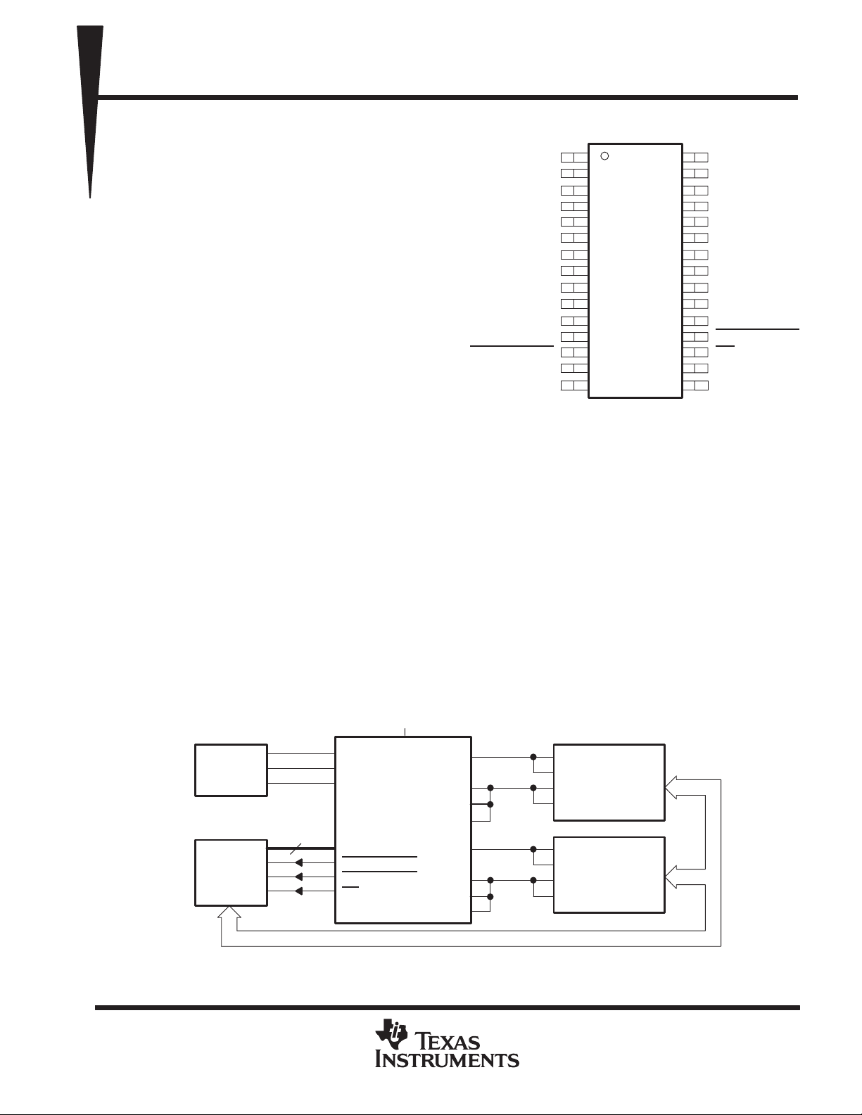
description
The TPS2202 PC Card (PCMCIA) power-interface switch provides an integrated power-management solution
for two PC Cards. All of the discrete power MOSFETs, a logic section, current limiting, thermal protection, and
power-good reporting for PC Card control are combined on a single integrated circuit (IC), using Texas
Instruments LinBiCMOS process. The circuit allows the distribution of 3-V, 5-V, and/or 12-V card power by
means of a reduced I/O serial interface. The current-limiting feature eliminates the need for fuses, which reduces
component count and improves reliability; current-limit reporting can help the user isolate a system fault to a
bad card.
DD
The TPS2202 maximizes battery life by using an internal charge pump to generate its own switch-drive voltage.
Therefore, the 12-V supply can be powered down and only brought out of standby when flash memory needs
to be written to or erased. End equipment for the TPS2202 includes notebook computers, desktop computers,
personal digital assistants (PDAs), digital cameras, handiterminals, and bar-code scanners.
typical PC-card power-distribution application
V
Power Supply
12 V
5 V
3 V
3
PCMCIA
Controller
LinBiCMOS is a trademark of Texas Instruments Incorporated.
PRODUCTION DATA information is current as of publication date.
Products conform to specifications per the terms of Texas Instruments
standard warranty. Production processing does not necessarily include
testing of all parameters.
12V
5V
3V
Serial Interface
APWR_GOOD
BPWR_GOOD
OC
DD
TPS2202
AVPP
AVCC
AVCC
AVCC
BVPP
BVCC
BVCC
BVCC
V
pp1
V
V
V
V
V
V
V
pp2
CC
CC
pp1
pp2
CC
CC
PC
Card A
PC
Card B
Copyright 1995, Texas Instruments Incorporated
POST OFFICE BOX 655303 • DALLAS, TEXAS 75265
6–1
Page 2
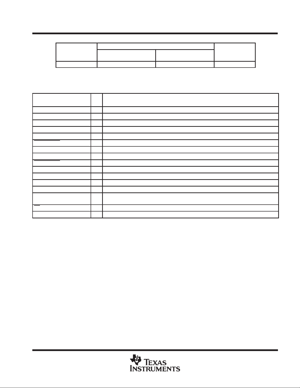
TPS2202, TPS2202Y
CHIP FORM
I/O
DESCRIPTION
DUAL-SLOT PC CARD POWER-INTERFACE SWITCHES
FOR SERIAL PCMCIA CONTROLLERS
SLVS103A – DECEMBER 1994 – REVISED AUGUST 1995
AVAILABLE OPTIONS
PACKAGED DEVICES
T
J
–40°C to 150°C TPS2202IDB TPS2202IDF TPS2202Y
†
The DF package is only available left-end taped and reeled (indicated by the LE suffix on the device type; e.g.,
TPS2202IDFLE).
TERMINAL
NAME NO.
3V 15, 16, 17 I 3-V VCC input for card power
5V 1, 2, 30 I 5-V VCC input for card power
12V 7, 24 I 12-V VPP input for card power
AVCC 9, 10, 11 O Switched output that delivers 0 V , 3.3 V, 5 V, or high impedance
AVPP 8 O Switched output that delivers 0 V, 3.3 V, 5 V, 12 V, or high impedance
APWR_GOOD 13 O Logic-level power-ready output that stays low as long as AVPP is within limits.
BVCC 20, 21, 22 O Switched output that delivers 0 V, 3.3 V, 5 V, or high impedance
BVPP 23 O Switched output that delivers 0 V, 3.3 V, 5 V, 12 V, or high impedance
BPWR_GOOD 19 O Logic-level power-ready output that stays low as long as BVPP is within limits.
CLOCK 4 I Logic-level clock for serial data word
DATA 3 I Logic-level serial data word
GND 12 Ground
LATCH 5 I Logic-level latch for serial data word
NC 6, 14, 26,
OC 18 O Logic-level overcurrent reporting output that goes low when an overcurrent condition exists.
V
DD
27, 28, 29
25 5-V power to chip
SHINK SMALL-OUTLINE
(DB)
Terminal Functions
No internal connection
SMALL-OUTLINE
(DF)
(Y)
6–2
POST OFFICE BOX 655303 • DALLAS, TEXAS 75265
Page 3
TPS2202, TPS2202Y
DUAL-SLOT PC CARD POWER-INTERFACE SWITCHES
FOR SERIAL PCMCIA CONTROLLERS
SLVS103A – DECEMBER 1994 – REVISED AUGUST 1995
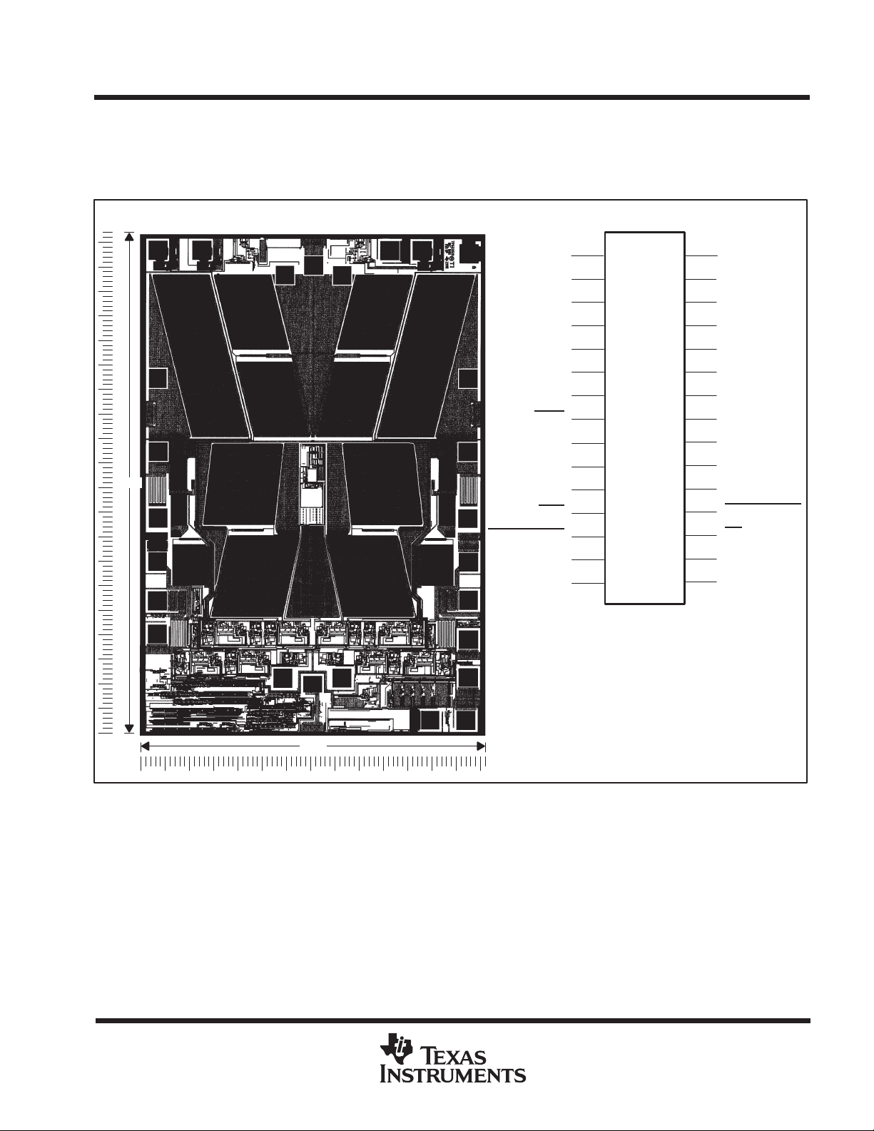
TPS2202Y chip information
This chip, when properly assembled, displays characteristics similar to the TPS2202. Thermal compression or
ultrasonic bonding may be used on the doped aluminum bonding pads. The chips may be mounted with
conductive epoxy or a gold-silicon preform.
BONDING PAD ASSIGNMENTS
204
(19)
(20)
(21)
(22)
(23)
(24)
(25)
(18)
(17)
(30)
(16)
(1)
142
(15)
(2)
(13)
(3) (4)
(12)
(11)
(10)
(9)
APWR_GOOD
(8)
(7)
(5)
(1)
(2)
5V
(3)
DATA
CLOCK
LATCH
(5)
(6)
NC
(7)
12V
(8)
AVPP
(9)
AVCC
(10)
AVCC
(11)
AVCC
(12)
GND
(13)
(14)
NC
(15)
3V
CHIP THICKNESS: 15 MILS TYPICAL
BONDING PADS: 4 × 4 MILS MINIMUM
TJmax = 150°C
TOLERANCES ARE ±10%
ALL DIMENSIONS ARE IN MILS
TERMINALS 6, 14, 26, 27, 28, AND 29
ARE NOT CONNECTED
TPS2201Y
(30)
(29)
(28)
(27)(4)
(26)
(25)
(24)
(23)
(22)
(21)
(20)
(19)
(18)
(17)
(16)
5V5V
NC
NC
NC
NC
V
DD
12V
BVPP
BVCC
BVCC
BVCC
BPWR_GOOD
OC
3V
3V
POST OFFICE BOX 655303 • DALLAS, TEXAS 75265
6–3
Page 4
TPS2202, TPS2202Y
Output current, I
DUAL-SLOT PC CARD POWER-INTERFACE SWITCHES
FOR SERIAL PCMCIA CONTROLLERS
SLVS103A – DECEMBER 1994 – REVISED AUGUST 1995
absolute maximum ratings over operating free-air temperature (unless otherwise noted)
Supply voltage range, V
Input voltage range for card power: V
–0.3 V to 7 V. . . . . . . . . . . . . . . . . . . . . . . . . . . . . . . . . . . . . . . . . . . . . . . . . . . . . . . . . .
DD
–0.3 V to 7 V. . . . . . . . . . . . . . . . . . . . . . . . . . . . . . . . . . . . . . . . . . . . .
I(5V)
V
–0.3 V to V
. . . . . . . . . . . . . . . . . . . . . . . . . . . . . . . . . . . . . . . . . . .
I(3V)
V
–0.3 V to 14 V. . . . . . . . . . . . . . . . . . . . . . . . . . . . . . . . . . . . . . . . . . .
I(12V)
†
Logic input voltage –0.3 V to 7 V. . . . . . . . . . . . . . . . . . . . . . . . . . . . . . . . . . . . . . . . . . . . . . . . . . . . . . . . . . . . . . . . .
Continuous total power dissipation See Dissipation Rating Table. . . . . . . . . . . . . . . . . . . . . . . . . . . . . . . . . . . . .
Output current (each card): I
O(xVCC)
I
O(xVPP)
Operating virtual junction temperature range, T
Operating free-air temperature range, T
Storage temperature range, T
stg
internally limited. . . . . . . . . . . . . . . . . . . . . . . . . . . . . . . . . . . . . . . . . . . . .
internally limited. . . . . . . . . . . . . . . . . . . . . . . . . . . . . . . . . . . . . . . . . . . . .
–40°C to 150°C. . . . . . . . . . . . . . . . . . . . . . . . . . . . . . . . . . . .
J
–40°C to 85°C. . . . . . . . . . . . . . . . . . . . . . . . . . . . . . . . . . . . . . . . . . . .
A
–55°C to 150°C. . . . . . . . . . . . . . . . . . . . . . . . . . . . . . . . . . . . . . . . . . . . . . . . . .
Lead temperature 1,6 mm (1/16 inch) from case for 10 seconds 260°C. . . . . . . . . . . . . . . . . . . . . . . . . . . . . . .
†
Stresses beyond those listed under “absolute maximum ratings” may cause permanent damage to the device. These are stress ratings only, and
functional operation of the device at these or any other conditions beyond those indicated under “recommended operating conditions” is not
implied. Exposure to absolute-maximum-rated conditions for extended periods may affect device reliability.
DISSIPATION RATING TABLE
PACKAGE
DB 1024 mW 8.2 mW/°C 655 mW 532 mW
DF 1158 mW 9.26 mW/°C 741 mW 602 mW
‡
Maximum values are calculated using a derating factor based on R
These devices are mounted on an FR4 board with no special thermal considerations.
TA ≤ 25°C
POWER RATING
DERATING FACTOR
ABOVE TA = 25°C
‡
TA = 70°C
POWER RATING
θJA
TA = 85°C
POWER RATING
= 108°C/W for the package.
I(5V)
recommended operating conditions
Supply voltage, V
Input voltage range, V
p
Clock frequency, f
Operating virtual junction temperature, T
†
V
should not be taken above V
I(3V)
O
DD
clock
V
I(5V)
I(5V)
V
I(3V)
V
I(12V)
I
O(xVCC)
I
O(xVPP)
J
.
I
MIN MAX UNIT
4.75 5.25 V
0 5.25 V
I(5V)
†
V
0 V
0 13.5 V
at 25°C 1 A
at 25°C 150 mA
0 2.5 MHz
–40 125 °C
6–4
POST OFFICE BOX 655303 • DALLAS, TEXAS 75265
Page 5
TPS2202, TPS2202Y
PARAMETER
TEST CONDITIONS
UNIT
mΩ
†
IppHigh-impedance state
Leakage current
A
ICCHigh-impedance state
Input current
Short-circuit output-current limit
J
,
PARAMETER
TEST CONDITIONS
UNIT
t
Output rise time
ms
t
Output fall time
ms
LATCH↑ to V
ms
t
Propagation delay (see Figure 1§)
LATCH↑ t
VCC (3 V)
ms
LATCH↑ to xVCC (5 V)
ms
DUAL-SLOT PC CARD POWER-INTERFACE SWITCHES
FOR SERIAL PCMCIA CONTROLLERS
SLVS103A – DECEMBER 1994 – REVISED AUGUST 1995
electrical characteristics, TA = 25°C, VDD = 5 V (unless otherwise noted)
dc characteristics
TPS2202
MIN TYP MAX
5 V to xVCC 160
3 V to xVCC 225
Switch resistances
Clamp low voltage Ipp at 10 mA 0.8 V
Clamp low voltage ICC at 10 mA 0.8 V
p
Power-ready threshold, PWR_GOOD 10.72 11.05 11.4 V
Power-ready hysteresis, PWR_GOOD (12-V mode) 50 mV
p
†
Pulse-testing techniques maintain junction temperature close to ambient temperature; thermal effects must be taken into account separately.
switching characteristics
r
f
pd
‡
Refer to Parameter Measurement Information
§
Propagation delays are with CL = 100 µF.
p
p
p
5 V to xVPP 6
3 V to xVPP 6
12 V to xVPP 1
p
p
I
DD
IDD in shutdown
I
O(xVCC)
I
O(xVPP)
TA = 25°C 1 10
TA = 85°C 50
TA = 25°C 1 10
TA = 85°C 50
V
O(AVCC)
V
O(AVPP)
V
O(BVCC)
T
Output powered up into a short to GND
= 85°C,
= V
= V
= V
= V
O(BVCC)
O(BVPP)
O(AVCC)
O(BVPP)
= 5 V,
= 12 V
= V
O(AVPP)
= high Z
83 150 µA
0.75 1.3 1.9 A
120 200 400 mA
‡
TPS2202
MIN TYP MAX
V
O(xVCC)
V
O(xVPP)
V
O(xVCC)
V
O(xVPP)
o x
O(xVPP)
t
on
t
off
t
on
t
off
t
on
t
off
1.2
5
10
14
5.8
18
5.8
28
4
30
µ
1 µA
Ω
POST OFFICE BOX 655303 • DALLAS, TEXAS 75265
6–5
Page 6
TPS2202, TPS2202Y
PARAMETER
TEST CONDITIONS
UNIT
I
1 mA
PARAMETER
TEST CONDITIONS
UNIT
Leakage current
A
PARAMETER
TEST CONDITIONS
UNIT
t
Output rise time
ms
t
Output fall time
ms
LATCH↑ to V
ms
t
Propagation delay (see Figure 1‡)
LATCH↑ t
VCC
ms
LATCH↑ to xVCC
ms
DUAL-SLOT PC CARD POWER-INTERFACE SWITCHES
FOR SERIAL PCMCIA CONTROLLERS
SLVS103A – DECEMBER 1994 – REVISED AUGUST 1995
electrical characteristics, TA = 25°C, VDD = 5 V (unless otherwise noted) (continued)
logic section
TPS2202
MIN MAX
Logic input current 1 µA
Logic input high level 2.7 V
Logic input low level 0.8 V
Logic output high level
Logic output low level
=
O
dc characteristics
IppHigh-impedance state 1
ICCHigh-impedance state 1
V
Input current I
Power-ready threshold, PWR_GOOD 11.05 V
Power-ready hysteresis, PWR_GOOD (12-V mode) 50 mV
DD
O(AVCC)
V
O(AVPP)
= V
= V
O(BVCC)
O(BVPP)
= 5 V,
= 12 V
VDD–0.4 V
0.4 V
TPS2202Y
MIN TYP MAX
83 µA
µ
switching characteristics
r
f
pd
†
Refer to Parameter Measurement Information
‡
Propagation delays are with CL = 100 µF.
p
p
p
†
V
O(xVCC)
V
O(xVPP)
V
O(xVCC)
V
O(xVPP)
o x
O(xVPP)
TPS2202Y
MIN TYP MAX
1.2
5
10
14
t
on
t
off
t
on
t
off
t
on
t
off
5.8
18
5.8
28
4
30
6–6
POST OFFICE BOX 655303 • DALLAS, TEXAS 75265
Page 7
DUAL-SLOT PC CARD POWER-INTERFACE SWITCHES
FOR SERIAL PCMCIA CONTROLLERS
SLVS103A – DECEMBER 1994 – REVISED AUGUST 1995
PARAMETER MEASUREMENT INFORMATION
TPS2202, TPS2202Y
LATCH
V
O(xVPP)
V
pp
LOAD CIRCUIT
50%
t
on
VOLTAGE WAVEFORMS
Serial-Interface Timing 2
xVCC Propagation Delay and Rise Times With 1-µF Load, 3-V Switch 3
xVCC Propagation Delay and Fall Times With 1-µF Load, 3-V Switch 4
xVCC Propagation Delay and Rise Times With 100-µF Load, 3-V Switch 5
xVCC Propagation Delay and Fall Times With 100-µF Load, 3-V Switch 6
xVCC Propagation Delay and Rise Times With 1-µF Load, 5-V Switch 7
xVCC Propagation Delay and Fall Times With 1-µF Load, 5-V Switch 8
xVCC Propagation Delay and Rise Times With 100-µF Load, 5-V Switch 9
xVCC Propagation Delay and Fall Times With 100-µF Load, 5-V Switch 10
xVPP Propagation Delay and Rise Times With 1-µF Load, 12-V Switch 11
xVPP Propagation Delay and Fall Times With 1-µF Load, 12-V Switch 12
xVPP Propagation Delay and Rise Times With 100-µF Load, 12-V Switch 13
xVPP Propagation Delay and Fall Times With 100-µF Load, 12-V Switch 14
C
L
V
t
off
90%
10%
DD
GND
V
I(12V)
GND
LATCH
V
O(xVCC)
t
on
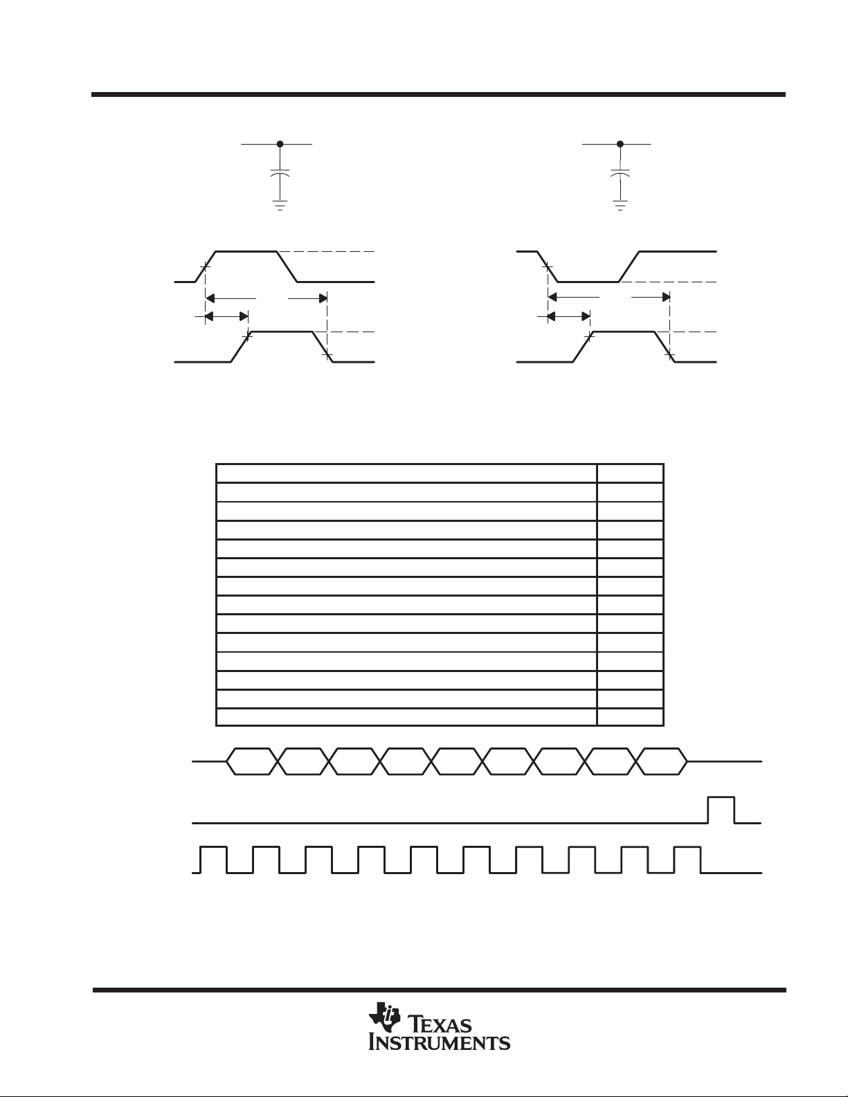
Figure 1. Test Circuits and Voltage Waveforms
Table of Timing Diagrams
V
CC
C
L
LOAD CIRCUIT
50%
t
off
90%
VOLTAGE WAVEFORMS
FIGURE
10%
V
DD
GND
V
I(5V)
GND
DATA
LATCH
CLOCK
NOTE A. Data is clocked in on the a positive leading edge of the clock. The latch should occur before next positive leading edge of
the clock. For definition of D0–D8, see control logic table.
D8 D7 D6 D5 D4 D3 D2 D1 D0
Figure 2. Serial-Interface Timing
POST OFFICE BOX 655303 • DALLAS, TEXAS 75265
6–7
Page 8

TPS2202, TPS2202Y
DUAL-SLOT PC CARD POWER-INTERFACE SWITCHES
FOR SERIAL PCMCIA CONTROLLERS
SLVS103A – DECEMBER 1994 – REVISED AUGUST 1995
PARAMETER MEASUREMENT INFORMATION
LATCH (2 V/div)
xVCC (1 V/div)
0123456789
t – Time – ms
Figure 3. xVCC Propagation Delay and
Rise Times With 1-µF Load, 3-V Switch
LATCH (2 V/div) LATCH (2 V/div)
LATCH (2 V/div)
xVCC (1 V/div)
0 5 10 15 20 25 30 35 40 45
t – Time – ms
Figure 4. xVCC Propagation Delay and
Fall Times With 1-µF Load, 3-V Switch
xVCC (1 V/div)
0123456789
t – Time – ms
Figure 5. xVCC Propagation Delay and
Rise Times With 100-µF Load, 3-V Switch
6–8
xVCC (1 V/div)
0 5 10 15 20 25 30 35 40 45
t – Time – ms
Figure 6. xVCC Propagation Delay and
Fall Times With 100-µF Load, 3-V Switch
POST OFFICE BOX 655303 • DALLAS, TEXAS 75265
Page 9

DUAL-SLOT PC CARD POWER-INTERFACE SWITCHES
FOR SERIAL PCMCIA CONTROLLERS
SLVS103A – DECEMBER 1994 – REVISED AUGUST 1995
PARAMETER MEASUREMENT INFORMATION
TPS2202, TPS2202Y
LATCH (2 V/div)
xVCC (1 V/div)
01234
t – Time – ms
Figure 7. xVCC Propagation Delay and
Rise Times With 1-µF Load, 5-V Switch
LATCH (2 V/div)
LATCH (2 V/div)
xVCC (1 V/div)
0 5 10 15 20 25 30 35 40 45
t – Time – ms
Figure 8. xVCC Propagation Delay and
Fall Times With 1-µF Load, 5-V Switch
xVCC (1 V/div)
LATCH (2 V/div)
xVCC (1 V/div)
0123456789
t – Time – ms
Figure 9. xVCC Propagation Delay and
Rise Times With 100-µF Load, 5-V Switch
POST OFFICE BOX 655303 • DALLAS, TEXAS 75265
0 5 10 15 20 25 30 35 40 45
t – Time – ms
Figure 10. xVCC Propagation Delay and
Fall Times With 100-µF Load, 5-V Switch
6–9
Page 10

TPS2202, TPS2202Y
DUAL-SLOT PC CARD POWER-INTERFACE SWITCHES
FOR SERIAL PCMCIA CONTROLLERS
SLVS103A – DECEMBER 1994 – REVISED AUGUST 1995
PARAMETER MEASUREMENT INFORMATION
xVPP (5 V/div)
LATCH (2 V/div)LATCH (2 V/div)
xVPP (5 V/div)
0 0.2 0.4 0.6 0.8 1.0 1.2 1.4 1.6 1.8
t – Time – ms t – Time – ms
Figure 11. xVPP Propagation Delay and
Rise Times With 1-µF Load, 12-V Switch
LATCH (2 V/div)
xVPP (5 V/div)
0123456789
t – Time – ms t – Time – ms
Figure 13. xVPP Propagation Delay and
Rise Times With 100-µF Load, 12-V Switch
0123456789
Figure 12. xVPP Propagation Delay and
Fall Times With 1-µF Load, 12-V Switch
LATCH (2 V/div)
xVPP (5 V/div)
0 5 10 15 20 25 30 35 40 45
Figure 14. xVPP Propagation Delay and
Fall Times With 100-µF Load, 12-V Switch
6–10
POST OFFICE BOX 655303 • DALLAS, TEXAS 75265
Page 11

TPS2202, TPS2202Y
DUAL-SLOT PC CARD POWER-INTERFACE SWITCHES
FOR SERIAL PCMCIA CONTROLLERS
SLVS103A – DECEMBER 1994 – REVISED AUGUST 1995
I
DD
r
DS(on)
r
DS(on)
r
DS(on)
V
O(xVCC)
V
O(xVCC)
xV
pp
I
SC(xVCC)
I
SC(xVPP)
TYPICAL CHARACTERISTICS
†
Table of Graphs
FIGURE
Supply current vs Junction temperature 15
Static drain-source on-state resistance, 3-V switch vs Junction temperature 16
Static drain-source on-state resistance, 5-V switch vs Junction temperature 17
Static drain-source on-state resistance, 12-V switch vs Junction temperature 18
Output voltage, 5-V switch vs Output current 19
Output voltage, 3-V switch vs Output current 20
Output voltage, Vpp switch vs Output current 21
Short-circuit current, 5-V switch vs Junction temperature 22
Short-circuit current, 12-V switch vs Junction temperature 23
SUPPLY CURRENT
vs
JUNCTION TEMPERATURE
100
V
O(AVCC)
V
O(AVPP)
No load
95
Aµ
= V
= V
O(BVCC)
O(BVPP)
= 5 V
= 12 V
90
85
– Supply Current –
DD
I
80
75
–50
TJ – Junction Temperature – °C
0 150
10050
Figure 15
†
t = pulse tested
POST OFFICE BOX 655303 • DALLAS, TEXAS 75265
6–11
Page 12

TPS2202, TPS2202Y
DUAL-SLOT PC CARD POWER-INTERFACE SWITCHES
FOR SERIAL PCMCIA CONTROLLERS
SLVS103A – DECEMBER 1994 – REVISED AUGUST 1995
TYPICAL CHARACTERISTICS
3-V SWITCH
STATIC DRAIN-SOURCE ON-STATE RESISTANCE
vs
Ω
400
VDD = 5 V
350
VCC = 3.3 V
300
250
200
150
100
50
– Static Drain-Source On-State Resistance – m
0
DS(on)
–50 0 125
r
JUNCTION TEMPERATURE
–25 25 50 75 100 –50 0 125
TJ – Junction Temperature – °C
†
5-V SWITCH
STATIC DRAIN-SOURCE ON-STATE RESISTANCE
vs
Ω
240
220
200
180
160
140
120
100
– Static Drain-Source On-State Resistance – mr
DS(on)
80
JUNCTION TEMPERATURE
VDD = 5 V
VCC = 5 V
–25 25 50 75 100
TJ – Junction Temperature – °C
Figure 16 Figure 17
12-V SWITCH
STATIC DRAIN-SOURCE ON-STATE RESISTANCE
vs
Ω
1700
VDD = 5 V
Vpp = 12 V
1500
1300
1100
900
700
– Static Drain-Source On-State Resistance – mr
500
–50 50 125
DS(on)
JUNCTION TEMPERATURE
–25 0 25 75 100
TJ – Junction Temperature – °C
5-V SWITCH
OUTPUT VOLTAGE
OUTPUT CURRENT
5.05
VDD = 5 V
VCC = 5 V
5
4.99
4.9
– Output Voltage – V
4.85
O(xVCC)
V
4.8
4.75
0 0.1 0.2 0.3 0.4 0.5
I
O(xVCC)
vs
–40°C
25°C
85°C
125°C
0.6 0.7
– Output Current – A
†
t = pulse tested
6–12
Figure 18 Figure 19
POST OFFICE BOX 655303 • DALLAS, TEXAS 75265
Page 13

TPS2202, TPS2202Y
DUAL-SLOT PC CARD POWER-INTERFACE SWITCHES
FOR SERIAL PCMCIA CONTROLLERS
SLVS103A – DECEMBER 1994 – REVISED AUGUST 1995
3.35
3.3
3.25
3.2
– Output Voltage – VV
3.15
O(xVCC)
3.1
3.05
OUTPUT CURRENT
0 0.1 0.2
I
O(xVCC)
3-V SWITCH
OUTPUT VOLTAGE
vs
125°C
0.3 0.4 0.6
– Output Current – A
TYPICAL CHARACTERISTICS
12.05
VDD = 5 V
VCC = 3.3 V
12
–40°C
25°C
85°C
0.70.5
11.95
11.90
– Output Voltage – V
pp
xV
11.85
11.80
0 0.02 0.04 0.06
†
Vpp SWITCH
OUTPUT VOLTAGE
OUTPUT CURRENT
I
O(xVPP)
– Output Current – A
vs
85°C
125°C
0.08 0.12
VDD = 5 V
Vpp = 12 V
–40°C
25°C
0.1
2
1.5
– Short-Circuit Current – AI
1
SC(xVCC)
0.5
VDD = 5 V
VCC = 5 V
Figure 20 Figure 21
5-V SWITCH
SHORT-CIRCUIT CURRENT
SHORT-CIRCUIT CURRENT
vs
JUNCTION TEMPERATURE
400
VDD = 5 V
Vpp = 12 V
350
300
250
– Short-Circuit Current – mAI
200
150
SC(xVPP)
050
TJ – Junction Temperature – °CT
100 150–50
100
JUNCTION TEMPERATURE
12-V SWITCH
vs
0–50 50 150
– Junction Temperature – °C
J
100
†
t = pulse tested
Figure 22 Figure 23
POST OFFICE BOX 655303 • DALLAS, TEXAS 75265
6–13
Page 14

TPS2202, TPS2202Y
DUAL-SLOT PC CARD POWER-INTERFACE SWITCHES
FOR SERIAL PCMCIA CONTROLLERS
SLVS103A – DECEMBER 1994 – REVISED AUGUST 1995
APPLICATION INFORMATION
overview
PC Cards were initially introduced as a means to add EEPROM (flash memory) to portable computers with
limited on-board memory. The idea of add-in cards quickly took hold: modems, wireless LANs, GPS systems,
multimedia, and hard-disk versions were soon available. As the number of PC Card applications grew, the
engineering community quickly recognized the need for a standard to ensure compatibility across platforms.
T o this end, the PCMCIA (Personal Computer Memory Card International Association) was established and was
comprised of members from leading computer, software, PC card, and semiconductor manufacturers. One key
goal was to realize the concept of plug and play – cards and hosts from different vendors should be compatible
and able to communicate with one another transparently.
PC Card power specification
System compatibility also means power compatibility . The most current set of specifications (PC Card Standard)
set forth by the PCMCIA committee states that power is to be transferred between the host and the card through
eight of the PC Card connector’s 68 pins. This power interface consists of two V
pins. Multiple V
and ground pins minimize connector-pin and line resistance. The two Vpp pins were originally
CC
specified as separate signals but are commonly tied together in the host to form a single node to minimize
voltage losses. Card primary power is supplied through the V
voltage is supplied through the V
pins. As each pin is rated to 0.5 A, VCC and Vpp can theoretically supply up
pp
pins; flash-memory programming and erase
CC
to 1 A, assuming equal pin resistance and no pin failure. A conservative design would limit current to 500 mA.
Some applications, however, require higher V
currents; disk drives, for example, may need as much as
CC
750-mA peak current to create the initial torque necessary to spin up the platter. V
are defined by flash-memory programming requirements, typically under 120 mA.
, two Vpp, and four ground
CC
currents, on the other hand,
pp
future power trends
The 1-A physical-pin current alluded to in the PC Card specification has caused some host-system engineers
to believe they are required to deliver 1 A within the voltage tolerance of the card. Future applications, such as
RF cards, could use the extra power for their radio transmitters. The 5 W needed for these cards will require
very robust power supplies and special cooling considerations. The limited number of host sockets that will be
able to support them makes the market for these high-powered PC Cards uncertain. The vast majority of the
cards require less than 600 mA continuous current and the trend is towards even lower-powered PC Cards that
will assure compatibility with a greater number of host systems. Recognizing the need for power derating, an
adhoc committee of the PCMCIA is currently working to limit the amount of steady-state dc current to the
PC Card to something less than the currently implied 1 A. If a system is designed to support 1 A, then the switch
r
, power supply requirements, and PC Card cooling need to be carefully considered.
DS(on)
designing around 1-A delivery
Delivering 1 A means minimizing voltage (and power) losses across the PC Card power interface, which
requires that designers trade off switch resistance and the cost associated with large-die (low r
DS(on)
transistors. The PC Card standard requires that 5 V ±5%, or 3.3 V ±0.3 V be supplied to the card. The
approximate 10% tolerance for the 3.3-V supply makes the 3.3-V r
less critical than the 5-V switch. A
DS(on)
conservative approach is to allow 2% for voltage-regulator tolerance and 1% for etch- and terminal-resistance
drops, which leaves 2% (100 mV) voltage drop for the 5-V switch, and at least 6% (198 mV) for the 3.3-V switch.
Calculating the r
DS(on)
necessary to support a 100 mV or 198 mV switch loss, using R = E/I and setting I = 1 A,
the 5-V and 3.3-V switches would need to be 100 mΩ and 198 mΩ respectively . One solution would be to pay
for a more expensive switch with lower r
. A second, less expensive approach is to increase the headroom
DS(on)
of the power supply–for example, to increase the 5-V supply 1.5% or to 5.075 ±2%. Working through the
numbers once more, the 2% for the regulator plus 1 % for etch and terminal losses leaves 97% or 4.923 V.
) MOSFET
6–14
POST OFFICE BOX 655303 • DALLAS, TEXAS 75265
Page 15

TPS2202, TPS2202Y
DUAL-SLOT PC CARD POWER-INTERFACE SWITCHES
FOR SERIAL PCMCIA CONTROLLERS
SLVS103A – DECEMBER 1994 – REVISED AUGUST 1995
APPLICATION INFORMATION
designing around 1-A delivery (continued)
The allowable voltage loss across the power distribution switch is now 4.923 V minus 4.750 V or 173 mV.
Therefore, a switch with 173 mΩ or less could deliver 1 A or greater. Setting the power supply high is a common
practice for delivering voltages to allow for system switch, connector, and etch losses and has a minimal ef fect
on overall battery life. In the example above, setting the power supply 1.5% high would only decrease a 3-hour
battery life by approximately 2.7 minutes, trivial when compared with the decrease in battery life when running
a 5-W PC Card.
heat dissipation
A greater concern in delivering 1 A or 5 W is the ability of the host to dissipate the heat generated by the PC
Card. For desktop computers the solution is simpler: locate the PC Card cage such that it receives convection
cooling from the forced air of the fan. Notebooks and other handheld equipment are not be able to rely on
convection, but must rely on conduction of heat away from the PC Card through the rails into the card cage. This
is difficult because PC Card/card cage heat transfer is very poor. A typical design scenario would require the
PC Card to be held at 60°C maximum with the host platform operating as high as 50°C. Preliminary testing
reveals that a PC Card can have a 20°C rise, exceeding the 10°C differential in the example, when dissipating
less than 2 W of continuous power. The 60°C temperature was chosen because it is the maximum operating
temperature allowable by PC Card specification. Power handling requirements and temperature rises are topics
of concern and are currently being addressed by the PCMCIA committee.
overcurrent and over-temperature protection
PC Cards are inherently subject to damage that can result from mishandling. Host systems require protection
against short-circuited cards that could lead to power supply or PCB-trace damage. Even systems sufficiently
robust to withstand a short circuit would still undergo rapid battery discharge into the damaged PC Card,
resulting in the rather sudden and unacceptable loss of system power. This can be particularly frustrating to the
consumer who has already experienced problems with shortened battery life due to improper Nicad conditioning
or memory effect. Most hosts include fuses for protection. The reliability of fused systems is poor, though, as
blown fuses require troubleshooting and repair, usually by the manufacturer . The TPS2202 takes a two-pronged
approach to overcurrent protection. First, instead of fuses, sense FETs monitor each of the power outputs.
Excessive current generates an error signal that linearly limits the output current, preventing host damage or
failure. Sense FET s, unlike sense resistors or polyfuses, have the added advantage that they do not add to the
series resistance of the switch and thus produce no additional voltage losses. Second, when an overcurrent
condition is detected, the TPS2202 asserts a signal at OC
diagnostics and/or send the user a warning message. In the event that an overcurrent condition persists,
causing the IC to exceed its maximum junction temperature, thermal-protection circuitry engages, shutting
down all power outputs until the device cools to within a safe operating region.
12-V supply not required
Most PC Card switches use the externally supplied 12-V V
functions, requiring that it be present at all times. The TPS2202 offers considerable power savings by using an
internal charge pump to generate the required higher voltages from the 5-V V
12-V supply can be disabled except when needed for flash-memory functions, thereby extending battery
lifetime. Additional power savings are realized by the TPS2202 during a software shutdown, in which quiescent
current drops to a maximum of 1 µA.
that can be monitored by the microprocessor to initiate
power for switch-gate drive and other chip
pp
supply; therefore, the external
DD
voltage transitioning requirement
PC Cards, like portables, are migrating from 5 V to 3.3 V to minimize power consumption, optimize board space,
and increase logic speeds. The TPS2202 is designed to meet all combinations of power delivery as currently
defined in the PCMCIA standard. The latest protocol accommodates mixed 3.3-V/5-V systems by first powering
the card with 5 V , then polling it to determine its 3.3-V compatibility . The PCMCIA specification requires that the
POST OFFICE BOX 655303 • DALLAS, TEXAS 75265
6–15
Page 16

TPS2202, TPS2202Y
DUAL-SLOT PC CARD POWER-INTERFACE SWITCHES
FOR SERIAL PCMCIA CONTROLLERS
SLVS103A – DECEMBER 1994 – REVISED AUGUST 1995
APPLICATION INFORMATION
voltage transitioning requirement (continued)
capacitors on 3.3-V compatible cards be discharged to below 0.8 V before applying 3.3-V power. This ensures
that sensitive 3.3-V circuitry is not subjected to any residual 5-V charge and functions as a power reset. The
TPS2202 offers a selectable V
specifications, to fully discharge the card capacitors while switching between V
output ground switches
Several PCMCIA power-distribution switches on the market do not have an active-grounding FET switch. These
devices do not meet the PC Card specification requiring a discharge of V
can not be relied on to provide a discharge path for voltages stored on PC Card capacitance because of possible
high-impedance isolation by power-management schemes. A method commonly shown to alleviate this
problem is to add to the switch output an external 100 kΩ resistor in parallel with the PC Card. Considering that
this is the only discharge path to ground, a timing analysis will reveal that the RC time constant delays the
required discharge time to over 2 seconds. The only way to ensure timing compatibility with PC Card standards
is to use a power-distribution switch that has an internal ground switch, like that of the TPS22xx family, or add
an external ground FET to each of the output lines with the control logic necessary to select it.
In summary, the TPS2202 is a complete single-chip dual-slot PC Card power interface. It meets all currently
defined PCMCIA specifications for power delivery in 5-V , 3.3-V , and mixed systems, and offers a serial controller
interface. The TPS2202 offers functionality, power savings, overcurrent and thermal protection, and fault
reporting in one 30-pin SSOP surface-mount package for maximum value added to new portable designs.
CC
and V
ground state, in accordance with PCMCIA 3.3-V/5-V switching
PP
within 100 ms. PC Card resistance
CC
voltages.
CC
power supply considerations
The TPS2202 has multiple terminals for each of its 3.3 V , 5 V, and 12 V power inputs and for the switched V
outputs. Any individual terminal can conduct the rated input or output current. Unless all terminals are connected
in parallel, the series resistance is significantly higher than that specified, resulting in increased voltage drops
and lost power. Both 12 V inputs must be connected for proper V
and output power terminals be paralleled for optimum operation. The V
5V input leads.
Although the TPS2202 is fairly immune to power input fluctuations and noise, it is generally considered good
design practice to bypass power supplies typically with a 1-µF electrolytic or tantalum capacitor paralleled by
a 0.047-µF to 0.1-µF ceramic capacitor. It is strongly recommended that the switched V
bypassed with a 0.1-µF or larger capacitor; doing so improves the immunity of the TPS2202 to electrostatic
discharge (ESD). Care should be taken to minimize the inductance of PCB traces between the TPS2202 and
the load. High switching currents can produce large negative-voltage transients, which forward biases substrate
diodes, resulting in unpredictable performance.
The TPS2202, unlike other PC Card power-interface switches, does not use the 12-V power supply for switching
or other chip functions. Instead, an internal charge pump generates the necessary voltage from V
the 12-V input supply to be shut down except when the V
programming or erase voltage is needed. Careful
pp
system design making use of this feature reduces power consumption and extends battery lifetime.
The 3.3-V power input should not be taken higher than the 5-V input. Doing so, though nondestructive, results
in high current flow into the device, and could result in abnormal operation. In any case, this occurrence indicates
a malfunction of one input voltage or both, which should be investigated.
Similarly, no terminal should be taken below –0.3 V; forward biasing the parasitic-substrate diode results in
substrate currents and unpredictable performance.
switching; it is recommended that all input
pp
input lead must be connected to the
DD
and Vpp outputs be
CC
, allowing
DD
CC
6–16
POST OFFICE BOX 655303 • DALLAS, TEXAS 75265
Page 17

TPS2202, TPS2202Y
DUAL-SLOT PC CARD POWER-INTERFACE SWITCHES
FOR SERIAL PCMCIA CONTROLLERS
SLVS103A – DECEMBER 1994 – REVISED AUGUST 1995
APPLICATION INFORMATION
overcurrent and thermal protection
The TPS2202 uses sense FET s to check for overcurrent conditions in each of the VCC and Vpp outputs. Unlike
sense resistors or polyfuses, these FETs do not add to the series resistance of the switch; therefore, voltage
and power losses are reduced. Overcurrent sensing is applied to each output separately . When an overcurrent
condition is detected, only the power output affected is limited; all other power outputs continue to function
normally. The OC
providing for initiation of system diagnostics and/or sending a warning message to the user.
indicator, normally a logic high, is a logic low when any overcurrent condition is detected,
During power up, the TPS2202 controls the rise time of the V
faulty card or connector. If a short circuit is applied after power is established (e.g., hot insertion of a bad card),
current is initially limited only by the impedance between the short and the power supply . In extreme cases, as
much as 10 A to 15 A may flow into the short before the current limiting of the TPS2202 engages. If the V
or Vpp outputs are driven below ground, the TPS2202 may latch nondestructively in an off state. Cycling power
reestablishes normal operation.
Overcurrent limiting for the V
0.75 A to 1.9 A, typically at about 1.3 A; the V
The protection circuitry acts by linearly limiting the current passing through the switch, rather than initiating a
full shutdown of the supply. Shutdown occurs only during thermal limiting.
Thermal limiting prevents destruction of the IC from overheating when the package power-dissipation ratings
are exceeded. Thermal limiting, disables all power outputs (both A and B slots) until the device has cooled.
outputs is designed to engage if powered up into a short in the range of
CC
outputs limit from 120 mA to 400 mA, typically around 200 mA.
pp
and Vpp outputs and limits the current into a
CC
calculating junction temperature
The switch resistance, r
is dependent on both r
16, 17, and 18 using an initial temperature estimate about 50°C above ambient. Then calculate the power
dissipation for each switch, using the formula:
PD+
r
DS(on)
Next, sum the power dissipation and calculate the junction temperature:
ǒ
S
TJ+
PD@
DS(on)
@
R
q
, is dependent on the junction temperature, TJ, of the die. The junction temperature
DS(on)
and the current through the switch. T o calculate TJ, first find r
2
I
JA
Ǔ
)
TA,R
q
JA
+
108 CńW
°
DS(on)
from Figures
CC
Compare the calculated junction temperature with the initial temperature estimate. If they are not within a few
degrees of each other, reiterate using the calculated temperature as the initial estimate.
logic input and outputs
The serial interface consists of DA T A, CLOCK, and LA TCH leads. The data is clocked in on the positive leading
edge of the clock (see Figure 2). The 9-bit (D0 through D8) serial data word is loaded during the positive edge
of the latch signal. The latch signal should occur before the next positive leading edge of the clock.
The shutdown bit of the data word places all V
quiescent current to 1 µA to conserve battery power .
The TPS2202 serial interface is designed to be compatible with serial-interface PCMCIA controllers and current
PCMCIA and JEIDA standards.
An overcurrent output (OC
as previously discussed.
) is provided to indicate an overcurrent condition in any of the VCC or Vpp outputs,
POST OFFICE BOX 655303 • DALLAS, TEXAS 75265
and Vpp outputs in a high-impedance state and reduces chip
CC
6–17
Page 18

TPS2202, TPS2202Y
DUAL-SLOT PC CARD POWER-INTERFACE SWITCHES
FOR SERIAL PCMCIA CONTROLLERS
SLVS103A – DECEMBER 1994 – REVISED AUGUST 1995
APPLICATION INFORMATION
TPS2202
S1
S2
3V
3V
3V
5V
5V
5V
15
16
17
1
2
30
S3
CS
CS
S4
CS
S5
S6
CS
S7
S8
S9
S10
S11
S12
8
9
10
11
20
21
22
23
18
52
17
51
17
51
18
52
Card A
VPP1
VPP2
VCC
VCC
Card B
VCC
VCC
VPP1
VPP2
Controller
12V
12V
24
19
13
18
7
Internal
Current Monitor
12
Thermal
25
V
DD
3
4
5
DATA
CLOCK
LATCH
BPWR_GOOD
APWR_GOOD
OC
Serial
Interface
GND
6–18
Figure 24. Internal Switching Matrix
POST OFFICE BOX 655303 • DALLAS, TEXAS 75265
Page 19

TPS2202, TPS2202Y
DUAL-SLOT PC CARD POWER-INTERFACE SWITCHES
FOR SERIAL PCMCIA CONTROLLERS
SLVS103A – DECEMBER 1994 – REVISED AUGUST 1995
APPLICATION INFORMATION
TPS2202 control logic
AVPP
CONTROL SIGNALS INTERNAL SWITCH SETTINGS OUTPUT
D8 SHDN D0 A_VPP_PGM D1 A_VPP_VCC S7 S8 S9 VAVPP
1 0 0 CLOSED OPEN OPEN 0 V
1 0 1 OPEN CLOSED OPEN VCC
1 1 0 OPEN OPEN CLOSED VPP(12 V)
1 1 1 OPEN OPEN OPEN Hi-Z
0 X X OPEN OPEN OPEN Hi-Z
BVPP
CONTROL SIGNALS INTERNAL SWITCH SETTINGS OUTPUT
D8 SHDN D4 B_VPP_PGM D5 B_VPP_VCC S10 S11 S12 VBVPP
1 0 0 CLOSED OPEN OPEN 0 V
1 0 1 OPEN CLOSED OPEN VCC
1 1 0 OPEN OPEN CLOSED VPP(12 V)
1 1 1 OPEN OPEN OPEN Hi-Z
0 X X OPEN OPEN OPEN Hi-Z
†
‡
A VCC
CONTROL SIGNALS INTERNAL SWITCH SETTINGS OUTPUT
D8 SHDN D3 A_VCC3 D2 A_VCC5 S1 S2 S3 VAVCC
1 0 0 CLOSED OPEN OPEN 0 V
1 0 1 OPEN CLOSED OPEN 3 V
1 1 0 OPEN OPEN CLOSED 5 V
1 1 1 CLOSED OPEN OPEN 0 V
0 X X OPEN OPEN OPEN Hi-Z
BVCC
CONTROL SIGNALS INTERNAL SWITCH SETTINGS OUTPUT
D8 SHDN D6 B_VCC3 D7 B_VCC5 S4 S5 S6 VBVCC
1 0 0 CLOSED OPEN OPEN 0 V
1 0 1 OPEN CLOSED OPEN 3 V
1 1 0 OPEN OPEN CLOSED 5 V
1 1 1 CLOSED OPEN OPEN 0 V
0 X X OPEN OPEN OPEN Hi-Z
†
Output depends on AVCC
‡
Output depends on BVCC
ESD protection
All TPS2202 inputs and outputs incorporate ESD-protection circuitry designed to withstand a 2-kV
human-body-model discharge as defined in MIL-STD-883C, Method 3015. The V
exposed to potentially higher discharges from the external environment through the PC Card connector.
Bypassing the outputs with 0.1-µF capacitors protects the devices from discharges up to 10 kV.
and Vpp outputs can be
CC
POST OFFICE BOX 655303 • DALLAS, TEXAS 75265
6–19
Page 20

TPS2202, TPS2202Y
DUAL-SLOT PC CARD POWER-INTERFACE SWITCHES
FOR SERIAL PCMCIA CONTROLLERS
SLVS103A – DECEMBER 1994 – REVISED AUGUST 1995
APPLICATION INFORMATION
5 V
V
DD
AVCC
0.1 µF
12 V
5 V
3 V
AVCC
12V
12V
TPS2202 0.1 µF
5V
5V
5V
3V
3V
3V
AVCC
BVCC
BVCC
BVCC
AVPP
AVPP
BVPP
BVPP
DATA
CLOCK
LATCH
0.1 µF
0.1 µF
V
CC
V
CC
V
pp1
V
pp2
V
CC
V
CC
V
pp1
V
pp2
DATA
CLOCK
LATCH
PC Card
Connector A
PC Card
Connector B
APWR_GOOD
BPWR_GOOD
To CPUOC
GND
Shutdown Signal
From CPU
AVPPGOOD
BVPPGOOD
Figure 25. Detailed Interconnections and Capacitor Recommendations
PCMCIA
Controller
CS
6–20
POST OFFICE BOX 655303 • DALLAS, TEXAS 75265
Page 21

IMPORTANT NOTICE
T exas Instruments and its subsidiaries (TI) reserve the right to make changes to their products or to discontinue
any product or service without notice, and advise customers to obtain the latest version of relevant information
to verify, before placing orders, that information being relied on is current and complete. All products are sold
subject to the terms and conditions of sale supplied at the time of order acknowledgement, including those
pertaining to warranty, patent infringement, and limitation of liability.
TI warrants performance of its semiconductor products to the specifications applicable at the time of sale in
accordance with TI’s standard warranty. T esting and other quality control techniques are utilized to the extent
TI deems necessary to support this warranty . Specific testing of all parameters of each device is not necessarily
performed, except those mandated by government requirements.
CERT AIN APPLICATIONS USING SEMICONDUCTOR PRODUCTS MAY INVOLVE POTENTIAL RISKS OF
DEATH, PERSONAL INJURY, OR SEVERE PROPERTY OR ENVIRONMENTAL DAMAGE (“CRITICAL
APPLICATIONS”). TI SEMICONDUCTOR PRODUCTS ARE NOT DESIGNED, AUTHORIZED, OR
WARRANTED TO BE SUITABLE FOR USE IN LIFE-SUPPORT DEVICES OR SYSTEMS OR OTHER
CRITICAL APPLICA TIONS. INCLUSION OF TI PRODUCTS IN SUCH APPLICATIONS IS UNDERST OOD TO
BE FULLY AT THE CUSTOMER’S RISK.
In order to minimize risks associated with the customer’s applications, adequate design and operating
safeguards must be provided by the customer to minimize inherent or procedural hazards.
TI assumes no liability for applications assistance or customer product design. TI does not warrant or represent
that any license, either express or implied, is granted under any patent right, copyright, mask work right, or other
intellectual property right of TI covering or relating to any combination, machine, or process in which such
semiconductor products or services might be or are used. TI’s publication of information regarding any third
party’s products or services does not constitute TI’s approval, warranty or endorsement thereof.
Copyright 1998, Texas Instruments Incorporated
 Loading...