

Datasheet TP30-68, TP30-62, TP30-270, TP30-240, TP30-220 Datasheet (SGS Thomson Microelectronics)
...Page 1
TP30-xxx Series
BIDIRECTIONALCROWBARPROTECTION.
VOLTAGERANGE: FROM62V TO 270 V.
HOLDINGCURRENT:
I
H
= 150mAmin.
REPETITIVEPEAKPULSECURRENT :
I
PP
=30 A,10/1000µs.
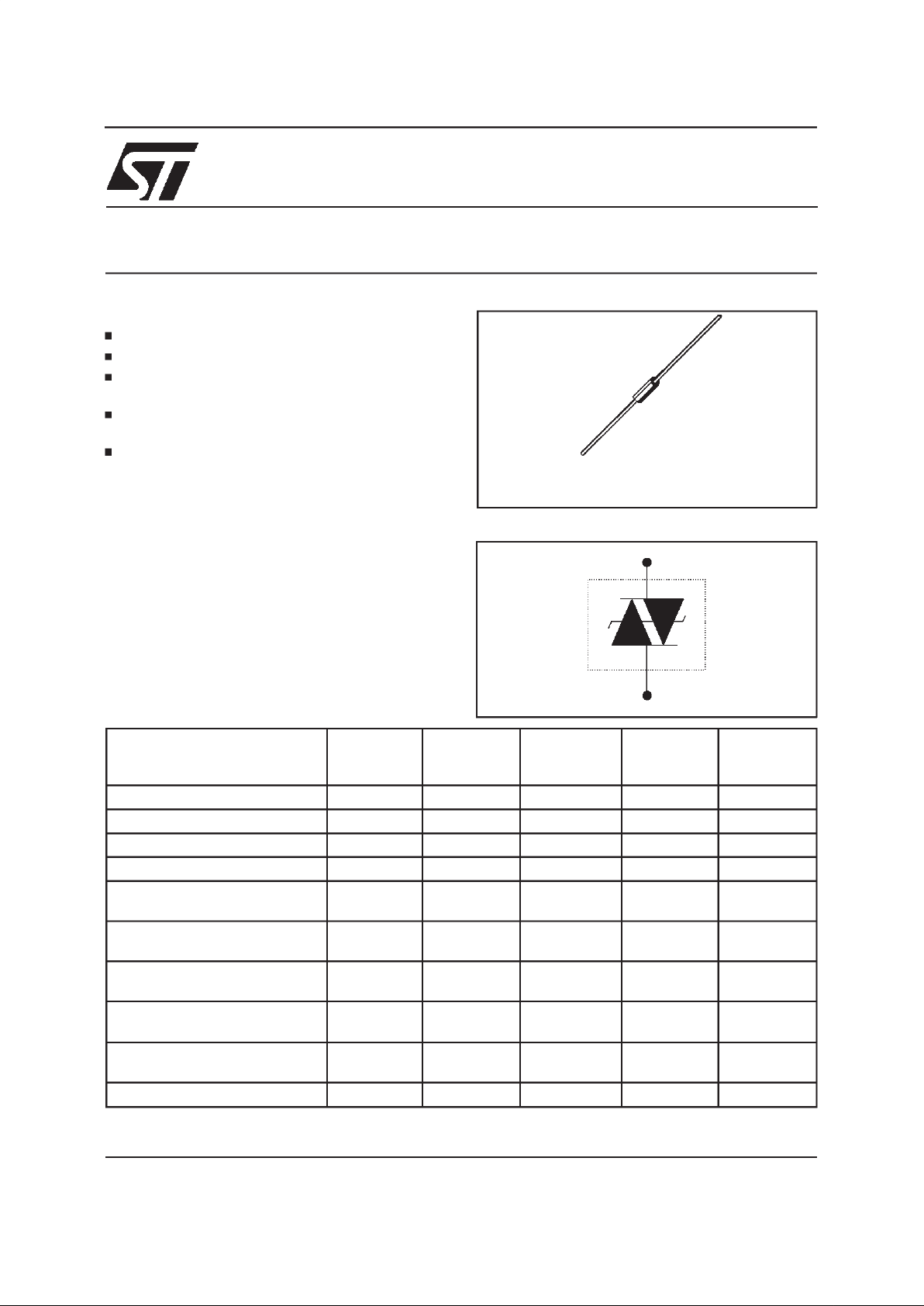
JEDECREGISTERED PACKAGEOUTLINE
FEATURES
F126
(JEDECDO-204AC)
TheTP30-xxx serieshasbeendesignedto protect
telecommunication equipment against lightning
surges and overvoltages induced by AC power
lines.
DESCRIPTION
SCHEMATIC DIAGRAM
TRISIL
TM
November 1998 - Ed: 5A
COMPLIESWITH THE
FOLLOWING STANDARDS:
Peak Surge
Voltage
(V)
Voltage
Waveform
(µs)
Current
Waveform
(µs)
Admissible
Ipp
(A)
Necessary
Resistor
(Ω)
(CCITT) ITU-K20 1000 10/700 5/310 25 (CCITT) ITU-K17 1500 10/700 5/310 38 VDE0433 2000 10/700 5/310 40 10
VDE0878 2000 1.2/50 1/20 50 IEC-1000-4-5 level2
level3
10/700
1.2/50
5/310
8/20
25
50
-
-
FCCPart68,lightningsurge
typeA
1500
800
10/160
10/560
10/160
10/560
65
50
15.5
8.0
FCCPart68,lightningsurge
typeB
1000 9/720 5/320 25 -
BELLCORETR-NWT-001089
Firstlevel
2500
1000
2/10
10/1000
2/10
10/1000
125
30
15.0
23.3
BELLCORETR-NWT-001089
Secondlevel
5000 2/10 2/10 125 15.0
CNETl31-24 1000 0.5/700 0.8/310 25 -
1/6
Page 2
Symbol Parameter Value Unit
R
th
(j-l)
Junction to leads
60 °C/W
R
th
(j-a)
Junctionto ambienton printedcircuit
withstandardfootprint dimension
100 °C/W
THERMAL RESISTANCES
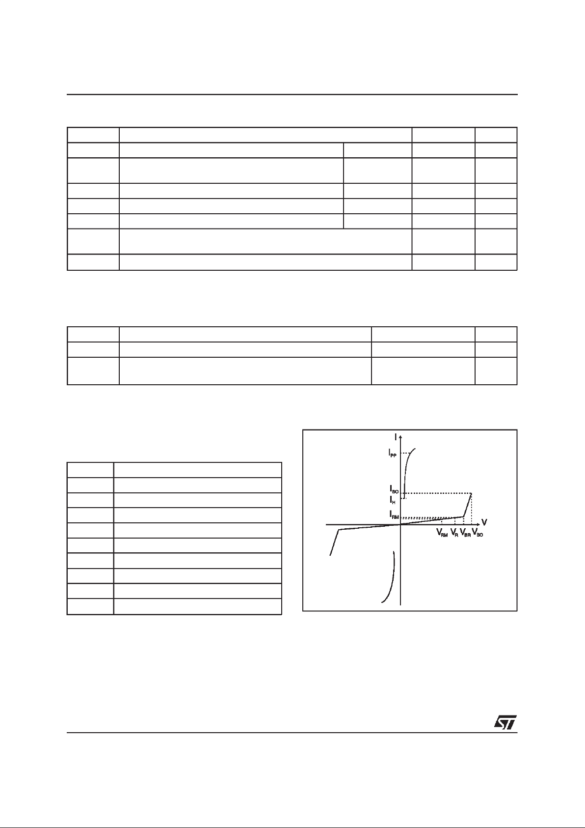
Symbol Parameter
V
RM
Stand-offvoltage
I
RM
Leakagecurrent at stand-offvoltage
V
R
ContinuousReverse voltage
V
BR
Breakdownvoltage
V
BO
Breakovervoltage
I
H
Holdingcurrent
I
BO
Breakovercurrent
I
PP
Peak pulse current
C Capacitance
ELECTRICALCHARACTERISTICS
(T
amb
=25°C)
Symbol Parameter Value Unit
P
Powerdissipationon infiniteheatsink
T
amb
=50 °C3 W
I
PP
Peak pulsecurrent 10/1000µs
8/20µs
30
60
A
I
TSM
Non repetitivesurge peak on-statecurrent tp= 20 ms 15 A
I
2
tI
2
t valueforfusing tp= 20 ms 1 A2s
dV/dt Criticalrateof riseof off-statevoltage V
RM
5 kV/µs
T
stg
T
j
Storagetemperaturerange
Maximumjunctiontemperature
- 55 to+ 150
150
°C
°C
T
L
Maximumleadtemperatureforsolderingduring10sat5mmforcase
230 °C
ABSOLUTE MAXIMUMRATINGS (T
amb
=25°C)
TP30-xxx Series
2/6
Page 3

Type IRM@V
RM
IR@V
R
VBO@I
BO
I
H
C
max max
note1
max
note 2
min
note3
typ
note4
typ
note 5
µAVµAV VmAmA pF
TP30-62
TP30-68
TP30-100
TP30-120
TP30-130
TP30-180
TP30-200
TP30-220
TP30-240
TP30-270
2
2
2
2
2
2
2
2
2
2
56
61
90
108
117
162
180
198
216
243
50
50
50
50
50
50
50
50
50
50
62
68
100
120
130
180
200
220
240
270
82
90
133
160
173
240
267
293
320
360
800
800
800
800
800
800
800
800
800
800
150
150
150
150
150
150
150
150
150
150
50
50
40
40
35
35
30
30
30
30
20
20
16
16
14
14
12
12
12
12
Note 1: IRmeasured at VRguarantee V
BRmin
≥ V
R
Note 2: Measured at 50 Hz (1 cycle) - Seetest circuit 1.
Note 3: See testcircuit 2.
Note 4: VR= 1V,F =1MHz.
Note 5: VR= 50V,F =1MHz.
TESTCIRCUIT 1 FORIBOandVBOparameters:
220V
static
relay.
R1
R2
240
140
D.U.T
V
BO
measure
I
BO
measure
tp
= 20ms
K
Transfor mer
220V/800V
5A
Auto
Transformer
220V/2A
V
out
TESTPROCEDURE :
PulseTestduration(tp= 20ms):
- For Bidirectionaldevices= SwitchK is closed
- For Unidirectionaldevices = Switch K is open.
V
OUT
Selection
- Devicewith V
BO
< 250 Volt
-V
OUT
= 250V
RMS,R1
=140Ω.
- Devicewith V
BO
≥ 250Volt
-V
OUT
= 480V
RMS,R2
= 240 Ω.
TP30-xxxSeries
3/6
Page 4

TESTCIRCUIT 2 forIHparameter.
R
-V
P
V
BAT
= - 48 V
Surge generator
D.U.T .
This is a GO-NOGOTest which allowsto confirmthe holdingcurrent (IH) level in a functional
test circuit.
TESTPROCEDURE:
1) Adjustthe currentlevel at the I
H
valuebyshortcircuiting the AKof the D.U.T.
2) Firethe D.U.Twith a surge Current : Ipp= 10A, 10/1000µs.
3) TheD.U.T will comebackoff-statewithin 50 ms max.
TP30-xxx Series
4/6
Page 5

1E-2 1E-1 1E+0 1E+1 1E+2 1E+3
0
5
10
15
20
t(s)
ITSM(A)
F = 50Hz
Fig. 1:
Non repetitivesurge peak on-sate current
versusoverload duration(Tj initial=25°C).
012345678910
1
2
5
10
20
50
VT(V)
IT(A)
Tj = 25°C
Fig. 4: On-state voltage versus on-state current
(typicalvalues).
-40 -20 0 20 40 60 80 100 120
0.0
0.2
0.4
0.6
0.8
1.0
1.2
1.4
1.6
1.8
2.0
Tj(°C)
IH[Tj] / IH[Tj=25°C]
Fig. 2:
Relativevariation of holdingcurrent versus
junctiontemperature.
1E-3 1E-2 1E-1 1E+0 1E+1 1E+2 5E+2
1E-1
1E+0
1E+1
1E+2
tp(s)
Zth(j-a)(°CW)
Fig. 5: Variationof thermalimpedance junctionto
ambientversus pulse duration.
1 10 100 300
0.1
0.2
0.5
1.0
VR(V)
C[VR]/C[VR=1V]
F =1MHz
Fig. 3: Relative variation of junction capacitance
versusreverse appliedvoltage(typicalvalues).
Note: ForVRM upper than 56V,thecurve is extrapolated (dottedline)
-40 -20 0 20 40 60 80 100
0.90
0.95
1.00
1.05
1.10
Tj(°C)
Vbo[Tj]/Vbo[Tj=25°C]
62 V
270V
Fig. 6:
Relative variation of V
BO
voltage versus
junctiontemperature.
TP30-xxxSeries
5/6
Page 6

Packaging: Tapeand reel.
Weight: 0.40g
Informationfurnished is believedtobeaccurate andreliable. However,STMicroelectronics assumesno responsIbility for theconsequences of
use ofsuch informationnor forany infringementof patentsorotherrights of thirdparties which may result fromitsuse. No licenseis grantedby
implication or otherwise under any patent or patent rights of STMicroelectronics. Specifications mentioned in this publication are subject to
change without notice. Thispublication supersedes and replaces all informationpreviously supplied.
STMicroelectronics products are not authorized for use as critical components in life support devices or systems without express written approval ofSTMicroelectronics.
The ST logo is a registered trademark of STMicroelectronics
1998 STMicroelectronics- Printed inItaly - All rights reserved.
STMicroelectronics GROUP OF COMPANIES
Australia - Brazil - Canada - China - France - Germany - Italy - Japan - Korea - Malaysia - Malta - Mexico - Morocco -
The Netherlands -Singapore - Spain - Sweden -Switzerland - Taiwan - Thailand - United Kingdom - U.S.A.
http://www.st.com
PACKAGEMECHANICALDATA
F126 (Plastic)(JEDEC DO-204AC)
A
CC
D
D
B
REF.
DIMENSIONS
Millimeters Inches
Min. Typ. Max. Min. Typ. Max.
A 6.05 6.20 6.35 0.238 0.244 0.250
B 2.95 3.00 3.05 0.116 0.118 0.120
C 26 31 1.024 1.220
D 0.76 0.81 0.86 0.030 0.032 0.034
ORDERCODE
TP 30 - 62
IPP=30 A
VOLTAGETRISILPROTECTION
MARKING :
Logo, Date Code, Part Number.
TP30-xxx Series
6/6
 Loading...