

Page 1
TP11368
Octal Adaptive Differential PCM Processor
TP11368 Octal Adaptive Differential PCM Processor
March 1997
General Description
The TP11368 is an octal (8) channel Adaptive Differential
Pulse Code Modulation (ADPCM) transcoder, fully compatible to ITU G.726 recommendation in 40 kbps, 32 kbps,
24 kbps, 16 kbps and ANSI 32 kbps modes. The TP11368
ADPCM processor can operate on up to 16 independent
channels in an 8 kHz frame. Each channel is individually
configured, supportingbothfull and half duplex operation. All
input/output transfers occur on an interrupt basis using serial, double buffered data registers. Together with National’s
TP3054/57 COMBO
TP11368 forms complete ADPCM channels with Codec/
filtering.
®
or TP3070/71 COMBO II devices, the
Block Diagram
Features
n CCITT G.726 compatible at 40, 32, 24, 16 kbps
n ANSI T1.301 compatible at 32 kbps
n 16-channel half-duplex (encode or decode) or 8-channel
full-duplex operation in 8 kHz frame
n Each channel individually configurable
n Selectable µ-law or A-law PCM coding
n Asynchronous 16 MHz master clock operation
n TTL and CMOS compatible inputs and outputs
n 28-pin PLCC or 24-pin DIP packages
n Power consumption of typ. 6 mW at +5V per full-duplex
channel
n On-Chip Power-On-Reset
n −40˚C to +85˚C operating temperature range
n Single 5V supply
DS012902-1
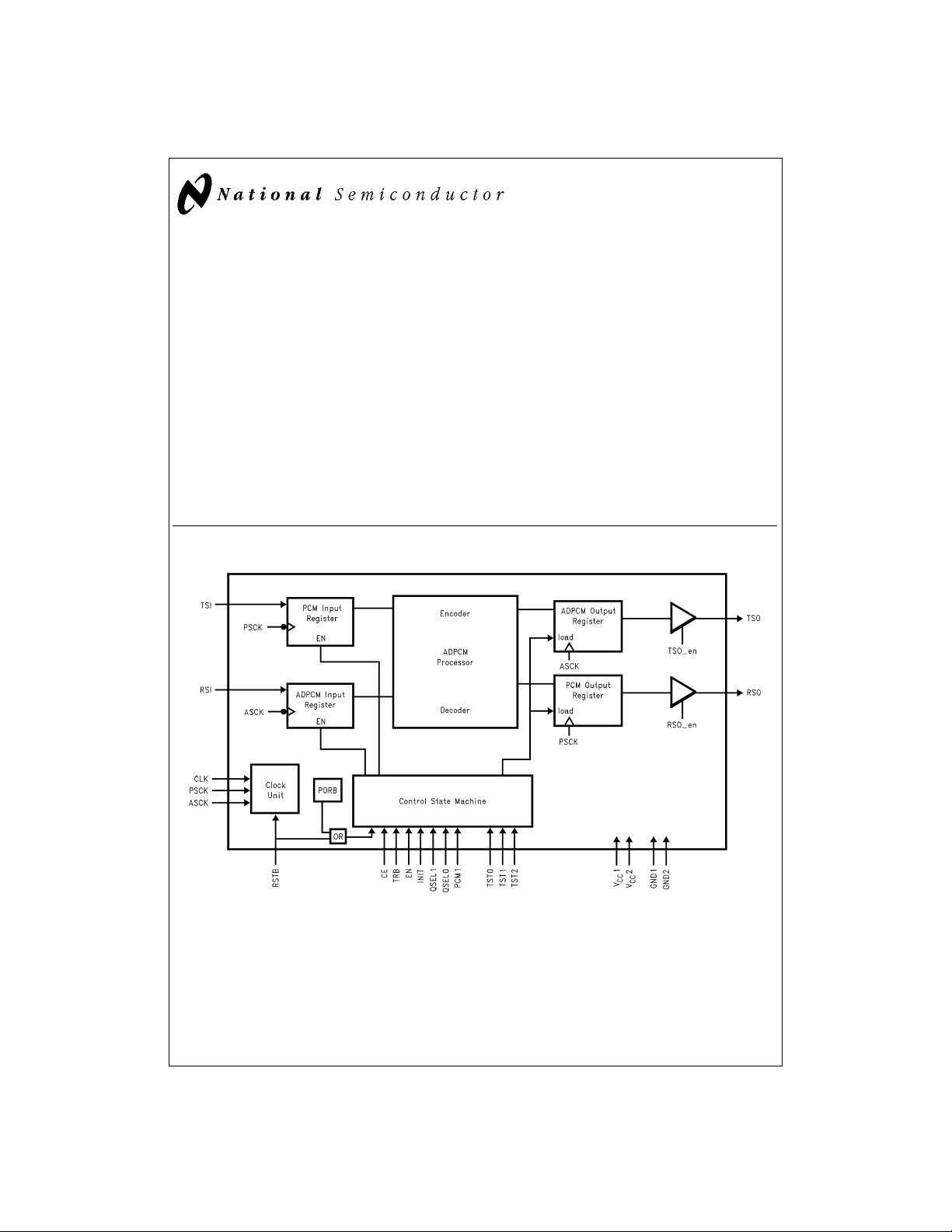
FIGURE 1. Block Diagram
TRI-STATE®and COMBO®are registered trademarks of National Semiconductor Corporation.
© 1997 National Semiconductor Corporation DS012902 www.national.com
Page 2
Connection Diagrams
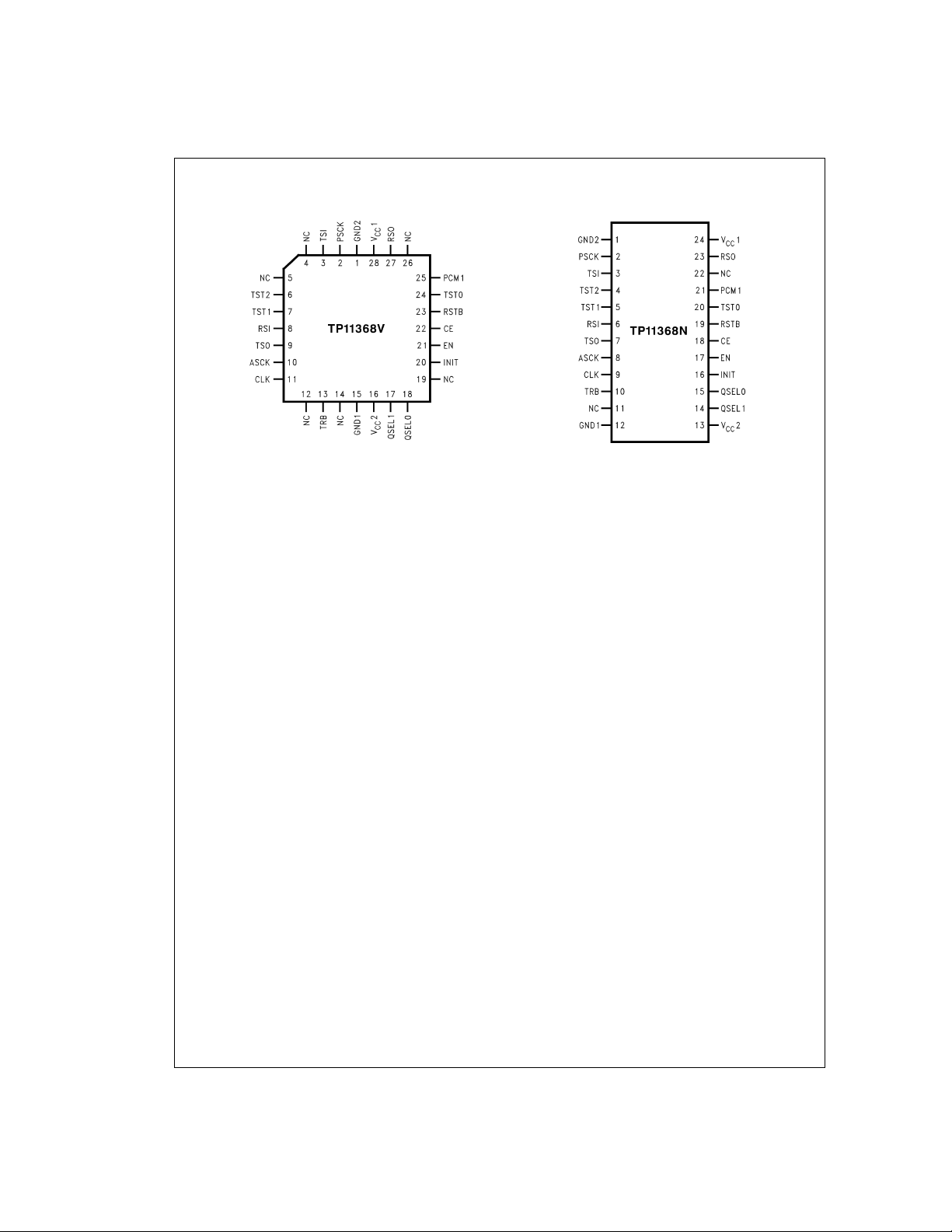
Plastic Chip Carrier
DS012902-2
Top View
Order Number TP11368V
See NS Package Number V28A
Pin Descriptions
TSI
Transmit PCM serial data input. TSI is an 8-bit PCM data
stream and is shifted into an 8-bit serial-to-parallel register
on the falling edges of PSCK while CE and TRB are high.
The last 8 bits of TSI are latched and transferred to the core
for processing at the falling edge of CE.
TSO
Transmit ADPCM TRI-STATE
data bit stream of 4- to 5-bit length, and is shifted out with the
rising edge of ASCK when CE is high following the processing of a transmit channel. TSO is in TRI-STATE mode while
CE is low or while RSO output is active.
RSI
ReceiveADPCM serial data input. RSI is a data bit stream of
4- to 5-bit length, and is shifted in with the falling edges of
ASCK while CE is high and TRB is low. The last 4 or 5 bits of
RSI are latched and transferred to the core for processing at
the falling edge of CE.
RSO
Receive PCM TRI-STATEserial data output. RSO is an 8-bit
PCM data stream and is shifted out with the rising edges of
PSCK when CE is high following the processing of a receive
channel. RSO is in TRI-STATEmode while CE is low or while
TSO output is active.
PSCK
PCM serial clock input. PSCK is used to shift PCM data into
TSI or out of RSO while CE is active (high). The transfer depends on the logic state of TRB.
ASCK
ADPCM serial clock input. ASCK is used to shift ADPCM
data into RSI or out of TSO while CE is active (high). The
transfer depends on the logic state of TRB.
®
serial data output. TSO is a
Plastic Dual-In-Line
DS012902-3
Top View
Order Number TP11368N
See NS Package Number N24A
CLK
Master clock input. CLK may be asynchronous to PSCK or
ASCK.
CE
Chip enable input. When CE is high, it enables data transfer.
The falling edge of CE latches and transfers the serial data
TSI or RSI to the core for processing and strobes the control
signals QSEL0, QSEL1, PCM1, EN and INIT. CE should
change state only when PSCK and ASCK are high. CE,
when low, sets the TSO and RSO outputs into TRI-STATE
mode.
TRB
Transmitter or receiver select. Alogic low at TRB selects the
receiver of the channel processed. A logic high enables the
transmitter of the channel processed. TRB determines which
input register is enabled and which output register and output is enabled. TRB should be stable while CE is high.
EN
Channel enable input. EN is strobed in with the falling edge
of CE. Alogic high at the falling edge of CE indicates that the
channel is active, and the ADPCM will process the data just
clocked in.
INIT
Channel initialization input. INIT is read at the falling edge of
CE.A logic high at the falling edge of CE causes the ADPCM
processor to initialize the channel currently processing.
PCM1
PCM coding law select. A logic low at PCM1 selects 8-bit
µ-law, while a logic high selects 8-bit A-law with even bit inversion.
www.national.com 2
Page 3
Pin Descriptions (Continued)
QSEL0, QSEL1
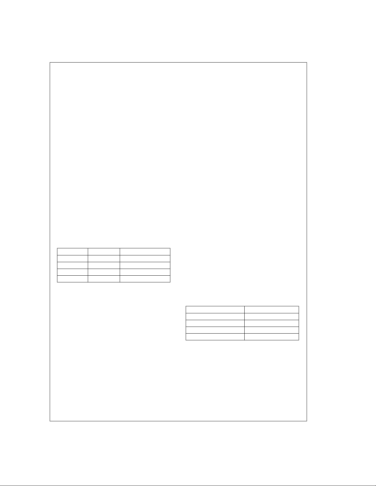
ADPCM bit rate select inputs. The QSEL0 and QSE1 signals
are strobed in with the falling edge of CE. The QSEL0 and
QSEL1 select the conversion bit rate of the PCM data just
clocked in at the TSI input or the bit rate of the ADPCM data
just clocked in at the RSI input. See
Table 1
.
RSTB
Chip reset input. A low to high transition at RSTB initiates the
reset sequence which initializes the channel variables for all
16 channels. A logic low applied to this pin sets the
transcoder into a low power dissipation mode. RSTB should
be pulled high for normal operation.
Functional Description
Adaptive Differential Pulse Code Modulation (ADPCM) is a
transcoding algorithm for voice and voice band data transmission. The use of ADPCM reduces the channel bandwidth
requirements from the standard 64 kbps PCM signal by a
factor of two or more. It is used for converting a 64 kbps
A-law or µ-law PCM channel to and from a 40, 32, 24 or
16 kbps channel. The8-bit PCM signal is reduced to 2–5bits
ADPCM signal depending on the selected bit rate in the encoder.
The TP11368 meets the ITU (CCITT) G.726 recommendation for 40, 32, 24, and 16 kbps ADPCM, as well as ANSI
T1.301 for 32 kbps. Each channel can be operated with an
independently selectable bit rate determined by QSEL1 and
QSEL0 (see
The ADPCM encoder converts the 64 kbps A-law or µ-law
PCM input signal to a uniform PCM signal which is subtracted from an estimated signal obtained from an adaptive
predictor. A 31-, 15-, 7-, or 4-level non-uniform quantizer is
used to assign five, four, three or two binary digits, respectively, to the value of the difference signal for transmission.
The ADPCM decoder reconstructs the original PCM signal
by adding the received quantized signal to the signal estimation calculated by the predictor. A synchronous coding adjustment unit prevents cumulative distortion occurring on
synchronous tandem codings (ADPCM-PCM-ADPCM) under certain conditions.
The adaptive predictor consists of two independent predictor
structures. One structure uses a second order recursive filter
which models the poles, and the other uses a sixth order
non-recursive filter which models the zeros in the input signal. This dual structure enables effective handling of both
speech and voice band data signals.
ADPCM PROCESSING
ADPCM to PCM Decoding Operation
When a logic “0” of TRB is latched in with the falling edge of
CE, the ADPCM processor is set to the decodingmode. Data
applied at the RSI input is sampled with the falling edge of
Table 1
).
TABLE 1. Bit Rate Selection
QSEL1 QSEL0 ADPCM Bit Rate
0 0 32 kbps
0 1 24 kbps
1 0 16 kbps
1 1 40 kbps
TST0, TST1, TST2
Test inputs for factory testing purposes. TST0–2 should be
tied low for normal operation.
V
CC1,VCC2
Positive power supply input pins. V
bypass capacitor should be connected between V
GND1, and V
and GND2.
CC2
=
±
5%. A 0.1 µF
5V
CC
CC1
and
GND1, GND2
Ground input pins.
NC
Not connected.
ASCK into a 5-bit ADPCM serial register. Within the next
cycle of CE, the decoder converts the ADPCM input data to
an 8-bit companded PCM data after 123 master clocks
(CLK). The 8-bit parallel PCM data is loaded into a
parallel-to-serial shift register and shifted out at the RSO output with the rising edges of PSCK.
PCM to ADPCM Encoding Operation
A logic “1” of TRB at the falling edge of CE sets the ADPCM
processor to the encoding mode. Data applied at the TSI input is sampled in an internal 8-bit PCM register with the falling edge of PSCK. During the next cycle of CE, the encoder
converts the companded 8-bit PCM data into a 5-, 4-, 3- or
2-bit ADPCM data, which will be shifted out during the third
cycle of CE at the TSO output with the rising edges ofASCK.
The TP11368 requires one master clock signal CLK. The
master clock signal CLK is not required to be synchronous to
the serial I/O clocks ASCK or PSCK. The serial interface
uses the serial clocks ASCK and PSCK and chip enable CE
for receiving and transmitting data. The data is internally
synchronized to the master clock CLK. There is a lower limit
of the clock frequency for CLK resulting from the number of
clock cycles required for processing the data.
Table2
shows
the required clock cycles per channel depending on the selected mode.
TABLE 2. Processing Cycles
Mode of Operation CLK Cycles Needed
Decoder 123
Encoder 123
Initialized Channel 45
Disabled Channel 4
The sampling period (usually 125 µs for 8 kHz frame) divided
by the number of CLK cycles gives the required minimum
CLK period. A slightly higher CLK frequency is used in order
to allow for jitter and inaccuracies in the CLK rate. As an example, for an eight channel ADPCM codec, CLK frequency
is 16 MHz as shown in the following calculations:
t
CLK
f
CLKmin
f
CLKnom
=
125 µs/(16
=
=
1/t
CLK
16.0 MHz
*
123)=63.5 ns
=
15.75 MHz
The period of CE must be equal to or greater than the required number of CLK cycles times the period of CLK. CE
must be low for more than 4 CLK cycles.
3 www.national.com
Page 4
Functional Description (Continued)
The TP11368is capable of processing 16 independent channels (half duplex) or 8 full-duplex PCM channels within 125
µs (8 kHz).
The logic state of TRB at the falling edge of CE determines
which input register is active during that CE period and which
output register will be active in the following third CE period.
The input data is processed (PCM data encoded or ADPCM
data decoded) during the second cycle and shifted out in the
third cycle of CE while CE is high.
SERIAL I/O
Input data is transferred into the TP11368on the falling edge
of the clock signal, while output data is transmitted on the rising edge of the clock signal. PCM data is transferred synchronously using PSCK, while ADPCM data is transferred
synchronously using ASCK. The clock signals ASCK and
PSCK should be high while CE changes. All serial data is
transferred with MSB first.
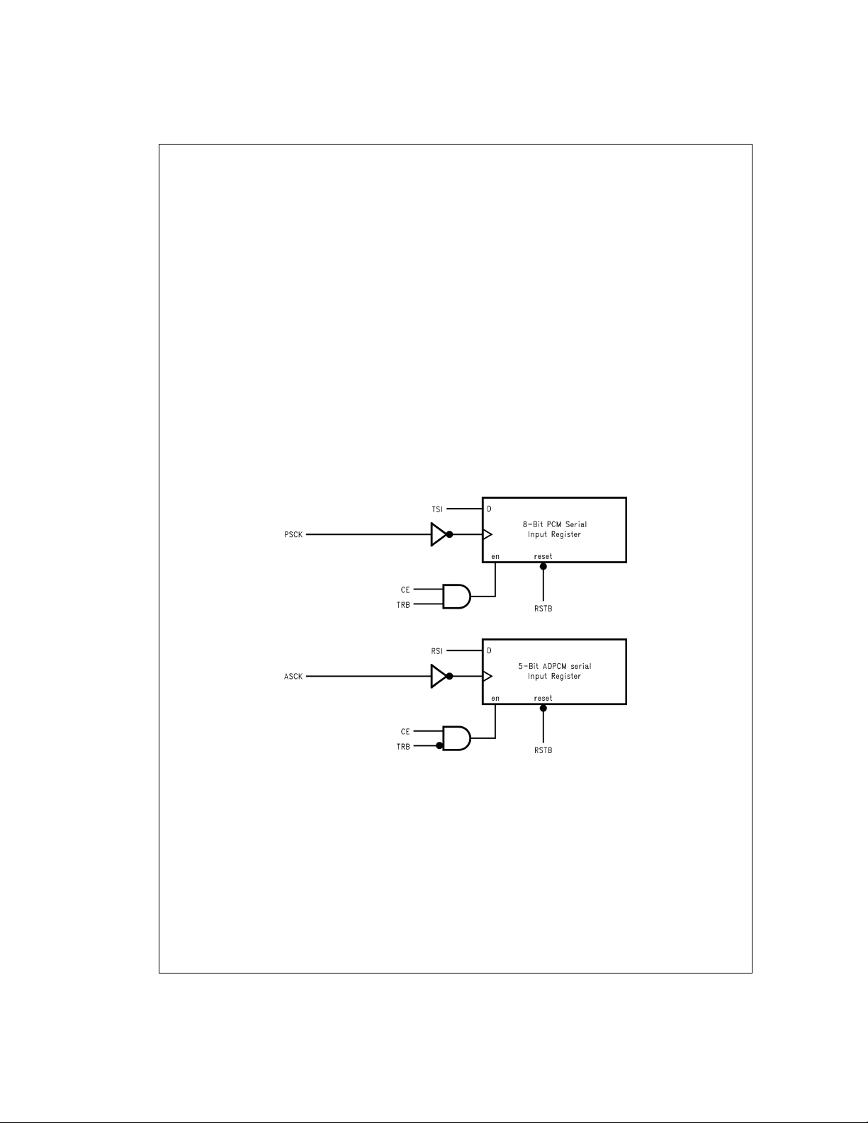
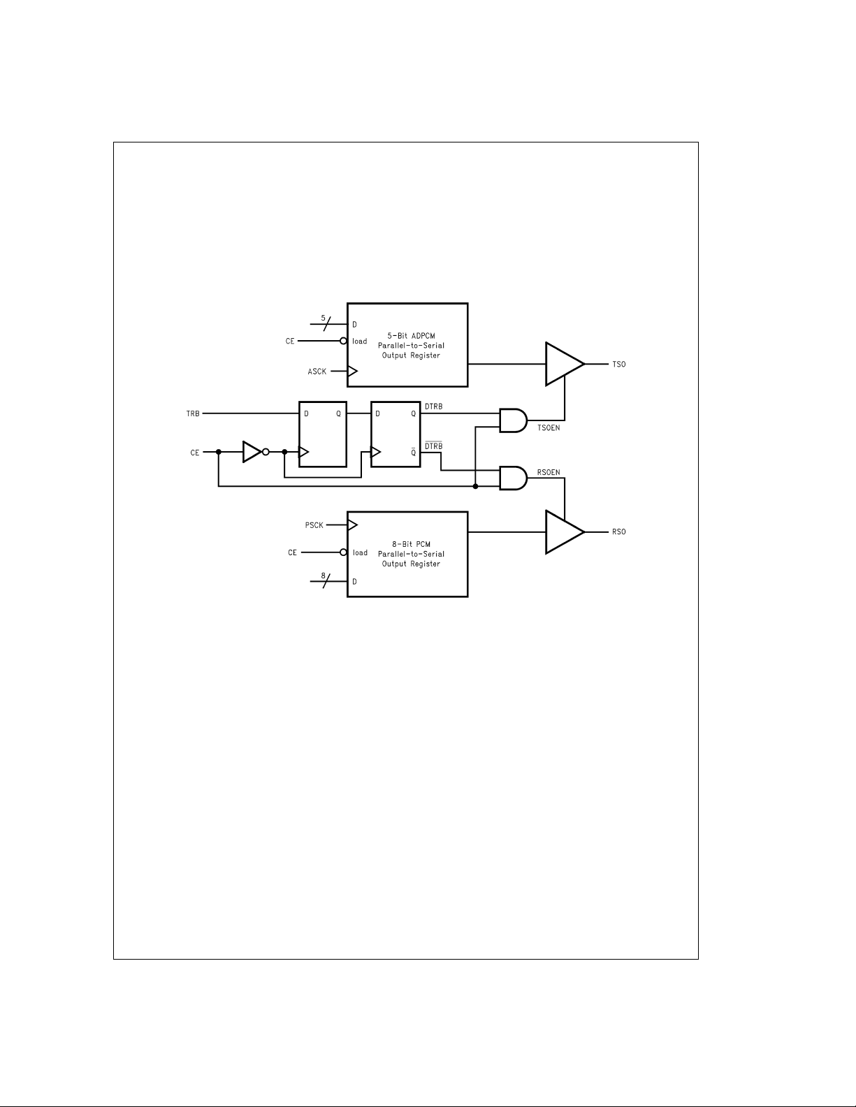
serial input and output structures, respectively.
PCM Serial Input Register
The serial PCM data to be encoded is shifted into the 8-bit
PCM input register with the falling edges of PSCK while CE
and TRB are high.The falling edge of CE latches the state of
Figure 2
and
Figure 3
show the
the input register and transfers the last 8 bits data prior to the
CE transition to the core for processing. The 8-bit PCM input
register is cleared asynchronously with RSTB going low.
ADPCM Serial Input Register
The ADPCM serial input register is a 5-bit shift register to
store the 5-bit data in the 40 kbpsADPCM mode. Serial input
data is latched in with the falling edges of ASCK while CE is
high and TRB is low. A minimum number of five low going
ASCK pulses must be available within the CE pulse when
operating in the 40 kbps mode. For the 32, 24 and 16 kbps
modes, a minimum of four low going ASCK pulses must be
available while CE is high. The falling edge of CE latches the
last 5 bits data in the 40 kbps mode or the last 4 bits data in
the 32, 24, and 16 kbps modes prior to the CE transistion.
See
Table 3
input register when 5ASCK low going pulses occur while CE
is high and TRB is low. Note that bit 1 in
for the position of the ADPCM data in the 5-bit
Table3
is the LSB.
FIGURE 2. Serial Input Structure
ADPCM Output Register
The internal encoded parallelADPCM data is loaded into the
5-bit ADPCM output register with the falling edge of CE signal. The first MSB data is shifted out after the rising edge of
CE, subsequent ADPCM serial data is shifted out with the
rising edge of ASCK.
ADPCM output data. If more than 4 ASCK clocks are available while CE is high in the 32, 24, and 16 kbps modes, the
ADPCM output data will recirculate starting with the MSB. In
the case of the 40 kbps mode, theADPCM output pattern will
recirculate, starting with the MSB, with the fifth rising edge of
ASCK while CE is high.
www.national.com 4
Table4
shows the transfer order of the
DS012902-4
PCM Output Register
The decoded 8-bit parallel PCM data is loaded into an 8-bit
parallel-to-serial output shift register with the falling edge of
CE. The MSB data is shifted out with the leading edge of CE,
and subsequent data are shifted out with the rising edges of
PSCK while CE is high. The 8-bit PCM data at the RSO output will recirculate with the MSB first after the seventh rising
edge of PSCK while CE is high.
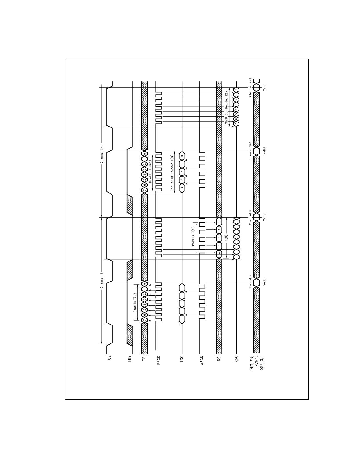
Figure 4
shows the full duplex timing diagram for the 40 kbps
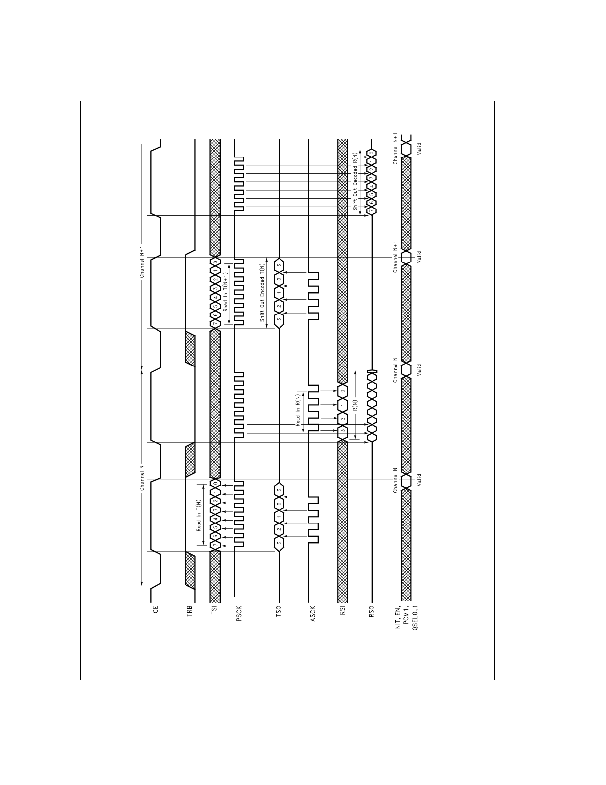
mode. For the 32, 24 and 16 kbps modes only fourASCK low
pulses are needed while CE is high (see
TRB is alternate high and low in the full duplex mode at each
falling edge of CE for a transmit (encoder) operation followed
Figure 5
).
Page 5
Functional Description (Continued)
by a receive (decoder) operation. For the encoding operation, the PCM data is stored in the 8-bit shift register at the
falling edge of CE while TRB is high. The TP11368 processes the data within 123 CLK periods during the following
cycle of CE. The encoded ADPCM data is loaded into the
5-bit parallel-to-serial output register with the falling edge of
CE. The MSB data is shifted out first with the leading edge of
CE, and subsequent data is shifted out with the rising edge
of ASCK. For the decoding operation, the ADPCM data is
latched and transferred to the core at the falling edge of CE
while TRB is low. The data is processed within 123 CLK periods and the decoded 8-bit PCM data is shifted out with the
MSB first.
PSCK and ASCK are the clocks for the PCM and ADPCM
data streams, respectively. They must be high during the
transition of CE. Note that PSCK and ASCK are shown as
gated clocks as an option to conserve power. PSCK and
ASCK need only be valid while CE is high.
FIGURE 3. Serial Output Structure
5 www.national.com
DS012902-5
Page 6
Functional Description (Continued)
DS012902-6
www.national.com 6
FIGURE 4. Full Duplex Timing Diagram (40 kbps ADPCM mode)
Page 7
Functional Description (Continued)
DS012902-7
Table3
shows the position of the ADPCM data in the 5-bit input register when five ASCK low going pulses are available
while CE is high. Only the last four bits of the ADPCM input
register prior to the falling edge of CE are latched in and
FIGURE 5. Full Duplex Timing Diagram (32 kbps ADPCM mode)
transferred to the core for processing in the 32, 24 and 16
kbps modes. In the 40 kbps mode, the last five bits prior to
7 www.national.com
Page 8
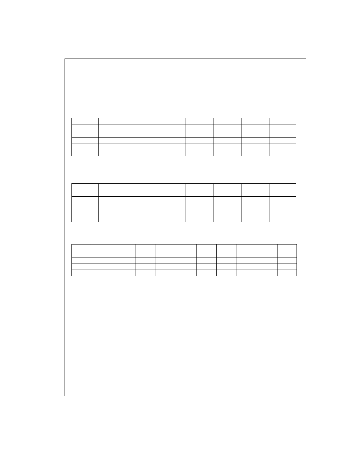
Table4
Functional Description (Continued)
the falling edge of CE are latched in. In
bit prior to to the CE falling edge is the LSB of the ADPCM
data word.
Note that the serial input data is referenced to the falling
edge of CE while the serial output data is referenced to the
Table3
, the last input
shows the transfer order of the ADPCM output data.
In the case where there are more ASCK clocks than the ADPCM data, the ADPCM output will recirculate.
For example, if the 32 kbps mode is selected, and eight low
pulses of ASCK exist within the CE high pulse, the following
ADPCM encoded data D3-D2-D1-D0-D3-D2-D1-D0 will appear at the TSO output (
Table 5
).
rising edge of CE.
TABLE 3. Transfer Order of ADPCM Input Data (RSI). The Last Bit Prior[to] the Falling Edge of CE is the LSB of the
ADPCM Data
QSEL1 QSEL0 Mode Bit 5 Bit 4 Bit 3 Bit 2 Bit 1
0 0 32 kbps x D3 D2 D1 D0
0 1 24 kbps x D2 D1 D0 x
1 0 16 kbps x D1 D0 x x
1 1 40 kbps D4 D3 D2 D1 D0
(MSB) (LSB)
Note 1: x=Don’t Care state
TABLE 4. Transfer Order of ADPCM Output Data (TSO) with 4 ASCK Rising Edgesile CE is High (the First Bit is the
MSB Data Bit following the Rising Edge of CE)
QSEL1 QSEL0 Mode Bit 5 Bit 4 Bit 3 Bit 2 Bit 1
0 0 32 kbps D3 D2 D1 D0 D3
0 1 24 kbps D2 D1 D0 x D2
1 0 16 kbps D1 D0 x x D1
1 1 40 kbps D4 D3 D2 D1 D0
(MSB) (LSB)
Note 2: x=unknown (but defined) state
TABLE 5. Transfer Order of ADPCM Output Data (TSO)th 7 Rising Edges (7 Low Pulses) while CE is High
QSEL1 QSEL0 Mode Bit 8 Bit 7 Bit 6 Bit 5 Bit 4 Bit 3 Bit 2 Bit 1
0 0 32 kbps D3 D2 D1 D0 D3 D2 D1 D0
0 1 24 kbps D2 D1 D0 x D2 D1 D0 x
1 0 16 kbps D1 D0 x x D1 D0 x x
1 1 40 kbps D4 D3 D2 D1 D0 D4 D3 D2
Note 3: x=unknown (but defined) state
SINGLE-CHANNEL INITIALIZATION AND
ALL-CHANNEL RESET
The TP11368 ADPCM processor can be initialized on a
per-channel basis via the use of INIT or on an all-channel basis via the use of RSTB. In both cases, the internal ADPCM
variables are initialized to the default values as suggested by
the ITU G.726 recommendation.
An individual channel can be initialized to the desired configuration by setting the corresponding data variables PCM1,
EN, QSEL(0,1) and by asserting the INIT pin high. The configuration data and INIT signal are strobed at the falling edge
of CE. For an initialization cycle, the period of CE must be 45
master clock (CLK) cycles. The transcoder is then ready to
process the next channel.
The active low RSTB signal is used for a “warm” reset as
well as for facilitating device testing. The initialization of the
internal memory takes 726 CLK cycles after the RSTB goes
inactive (logic “1”). The first transition of CE is allowed six
that CE be kept low during the initialization phase.The recommended values for ASCK and PSCK during initialization
are logic “1”, and that for TSI and RSI logic “0”. Any data (TSI
and RSI) applied during the initialization phase will be lost,
however, they won’t affect the proper initialization process.
The minimum low time of RSTB is 2 CLK cycles.
The chip resumes operation on the first negative edge of CE
after the completion of the initialization.
POWER-ON-RESET
The on-chip Power-On-Reset macro is activated when external power is first applied to the device. It has the same function as the external RSTB pin which initializes all channels to
the default values defined in the ITU Recommendation
G.726. At power up, the outputs TSO and RSO are in
TRI-STATEmode. This “cold” reset process is asynchronous
and takes approximately 2000 CLK cycles for the initialization.
CLK cycles after RSTB goes inactive. It is recommended
www.national.com 8
Page 9
Functional Description (Continued)
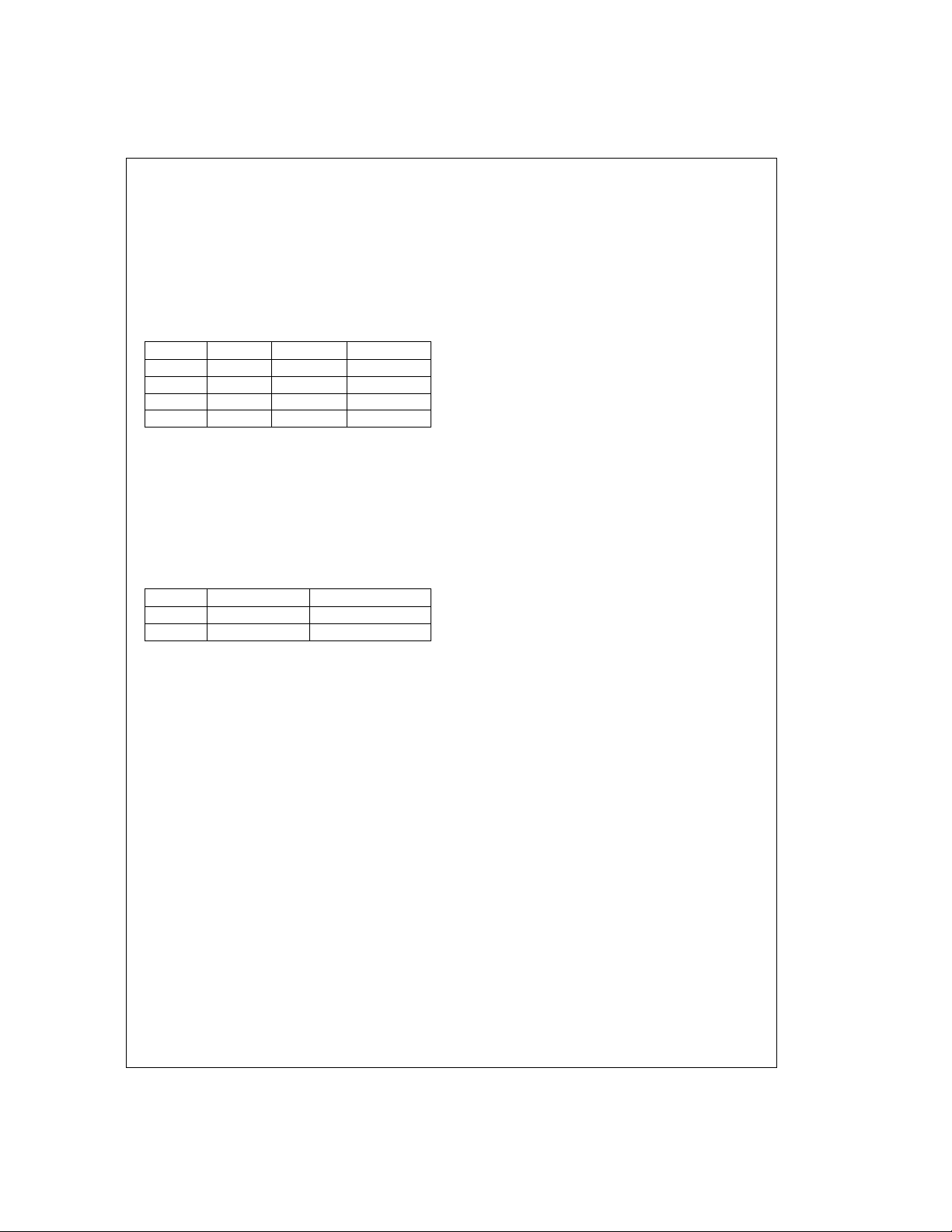
CHANNEL NOP
Each channel can be independently disabled. When EN is at
logic low on the falling edge of CE, the ADPCM transcoder
processing for that channel is disabled. The processor requires 4 CLK cycles for CE to maintain all channel variables.
The data output ports are also placed in known states. After
this the processor waits for the next interrupt. TSO outputs
the following data after a channel NOP:
TABLE 6. TSO at Channel NOP
QSEL1 QSEL0 Mode TSO
0 0 32 kbps 0000
0 1 24 kbps 0000
1 0 16 kbps 0000
1 1 40 kbps 00000
The data pattern at TSO in
ASCK clocks within the CE high pulse for the 32- , 24-,
16-kbps modes and five ASCK clocks within the CE high
pulse for the 40 kbps mode. In the case where ASCK pulses
are more than four or five, the given pattern recirculates with
the MSB first.
In the idle state, RSO outputs the following data (bit representation with the sign-bit on the left followed by the MSB,
the sign-bit is the first bit after the rising edge of CE):
TABLE 7. RSO at Channel NOP
PCM1 Mode RSO
0 8-Bit µ-Law 11111111
1 8-Bit A-Law 11010101
Table 6
are shown with four
9 www.national.com
Page 10
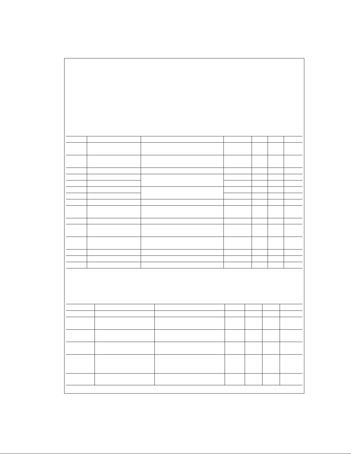
Absolute Maximum Ratings (Note *NO
TGT: FNXref NS0466*)
If Military/Aerospace specified devices are required,
please contact the National Semiconductor Sales Office/
Distributors for availability and specifications.
V
to GND 7V
CC
Voltage at Any Digital
Inputs or Outputs GND − 0.3V to V
CC
+ 0.3V
Storage Temperature Range −45˚C to +125˚C
Lead Temperature
(Soldering, 10 sec) 300˚C
±
Latch-up Immunity on any Pin
(28-pin PLCC) 79˚C/W
θ
JA
(24-pin DIP) 49˚C/W
θ
JA
75 mA
DC Electrical Characteristics
=
Unless otherwise noted, limits printed in bold characters are guaranteed forV
−40˚C to +85˚C by correlation with 100%electrical testing at T
production tests and/or product design and characterization. Typical values are specified at V
=
25˚C. All other limits are assured by correlation with other
A
CC
±
5%, GND1=GND2=0V, T
5.0V
=
+5V, T
CC
=
25˚C.
A
Symbol Parameter Conditions Min Typ Max Units
I
CC0
Supply Current CLK=16.0 MHz, RSTB=Low 1.8 mA
(Power Down Mode)
I
CC1
Supply Current CLK=16.0 MHz, RSTB=High 10 12 mA
(Power Up Mode)
P
D
V
IL
V
IH
V
IL
V
IH
V
OL
V
OH
I
IL
I
IH
Power Dissipation 50 mW
Input Low Voltage For ASCK, PSCK, CE, TRB, 0.8 V
Input High Voltage CLK, RSTB 2.4 V
Input Low Voltage For PCM1, RSI, TSI, QSEL0, 0.7 V
Input High Voltage QSEL1, INIT, EN 2.0 V
Output Low Voltage I
Output High Voltage I
Input Low Current GND<V
Input High Current V
=
4mA 0.4 V
L
=
−4 mA 2.4 V
L
=
I
L
<
IH
−0.4 mA; V
V
IN
=
4.75V V
CC
<
VIL, All Signal Inputs −10 µA
IN
<
VCC, All Signal Inputs 10 µA
− 0.8 V
CC
Test Inputs TST0, TST1, TST2 (Note 4) 150 µA
I
OZ
Output Current in High GND<V
<
VCC, TSO and RS0 −10 10 µA
O
Impedance State
C
I
C
O
C
L
Note 4: Test inputs have internal pull-down resistor.
Input Capacitance 10 pF
Output Capacitance 10 pF
Capacitive Load 100 pF
=
A
Timing Specifications
=
Unless otherwise noted, limits printed in bold characters are guaranteed for V
−40˚C to +85˚C by correlation with 100%electrical testing at T
production tests and/or product design and characterization. Typical values are specified at V
=
25˚C. All other limits are assured by correlation with other
A
CC
Symbol Parameter Conditions Min Typ Max Units
f
CLK
t
CLK
t
r
CLK Frequency (Note 5) Assuming 50%Duty Cycle 15.8 16 18 MHz
CLK Duty-Cycle 40
Rise Time (CLK, CE, 10 ns
ASCK, PSCK)
t
f
Fall Time (CLK, CE, 10 ns
ASCK, PSCK)
t
CEP
CE Period Encode or Decode 123 CLK
Initialization 45 Cycles
Disable 9
t
CEL
www.national.com 10
CE Pulse Width, Low 4 CLK
±
5%, GND1=GND2=0V, T
5.0V
=
+5V, T
CC
%
50
=
25˚C.
A
%
%
60
=
A
CLK
Period
Cycles
Page 11
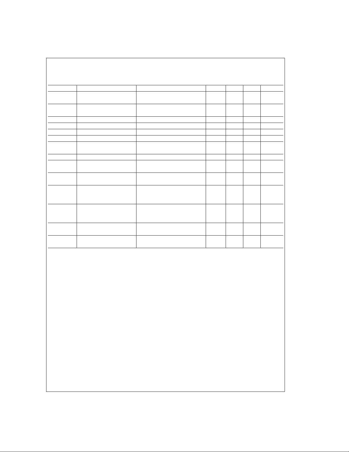
Timing Specifications (Continued)
=
Unless otherwise noted, limits printed in bold characters are guaranteed for V
−40˚C to +85˚C by correlation with 100%electrical testing at T
production tests and/or product design and characterization. Typical values are specified at V
=
25˚C. All other limits are assured by correlation with other
A
CC
Symbol Parameter Conditions Min Typ Max Units
t
HDCEL
Hold Time, CE low after 15 ns
PSCK/ASCK High
t
SUCEH
Setup Time, CE High Before 15 ns
PSCK/ASCK Low
t
TRBH
t
TRBS
t
IS
t
IH
t
PSCK/ASCK
TRB Hold Time From CE Low 20 ns
TRB Setup Time From ASCK Low and PSCK Low 20 ns
TSI, RSI Setup Time From ASCK Low and PSCK Low 20 ns
TSI, RSI Hold Time From ASCK Low and PSCK Low 20 ns
PSCK/ASCK High and 55 ns
Low Times
t
ON
t
OD
TSO, RSO Turn On Time From CE High 40 ns
TSO, RSO Propagation From ASCK High or PSCK High 40 ns
Delay Time
t
OFF
TSO, RSO Turn Off Time From CE Low 20 ns
(Valid Data to TRI-STATE)
t
CS
Setup Time for Control From CE Low
Signals (INIT, EN, 20 ns
PCM1, QSEL1, QSEL0)
t
CH
Hold Time for Control From CE Low
Signals (INIT, EN, 20 ns
PCM1, QSEL1, QSEL0)
t
RSTL
t
RSTH
RSTB Pulse Width Low 2 CLK
RSTB High to the First 6 CLK
CE High-Low Transition Cycles
Note 5: Values for 8 full-duplex (decoding and encoding) or 16 half-duplex (decoding or encoding) channels operation in a 125 µs period.
±
5%, GND1=GND2=0V, T
5.0V
=
+5V, T
CC
=
25˚C.
A
=
A
Cycles
11 www.national.com
Page 12
Timing Specifications (Continued)
DS012902-8
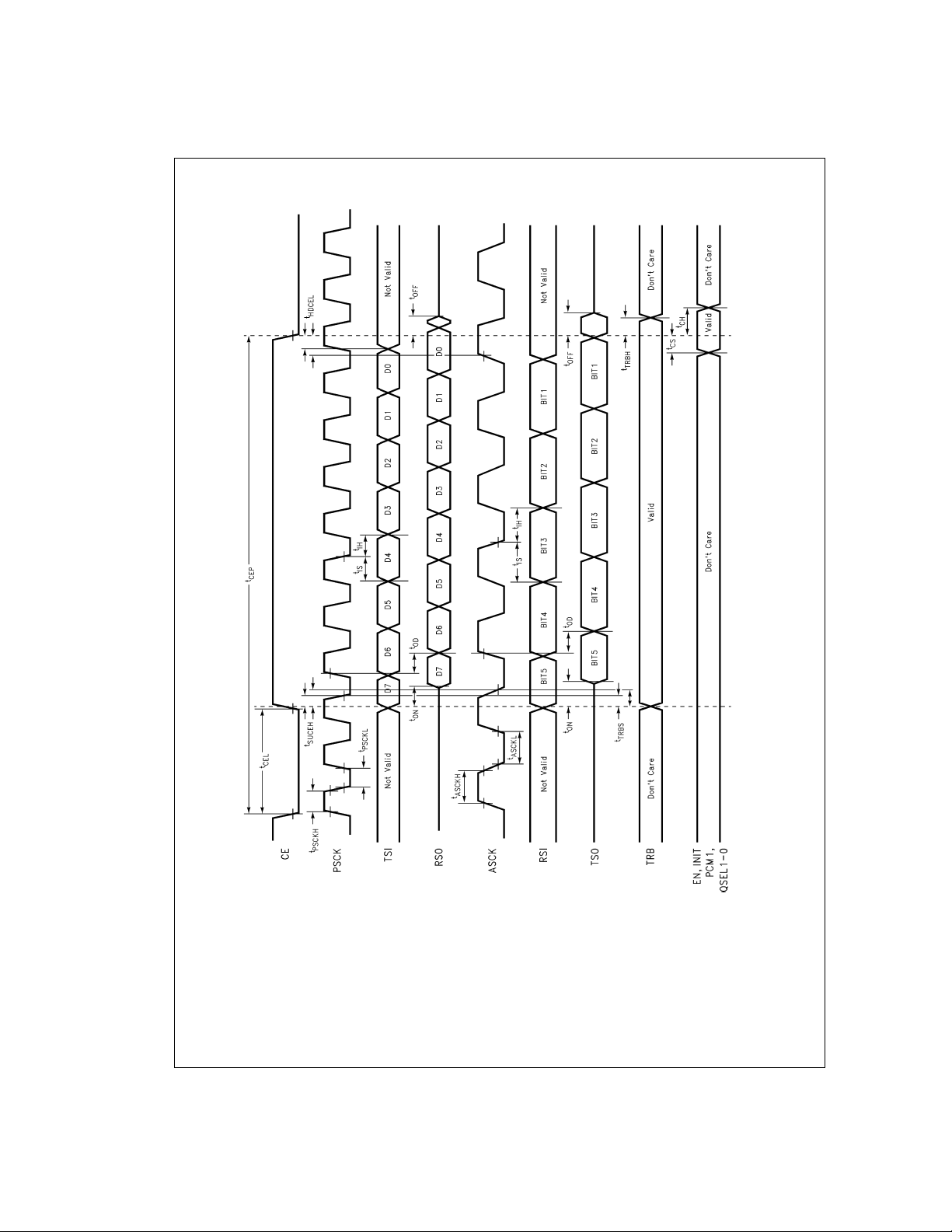
FIGURE 6. ADPCM Timing
www.national.com 12
Page 13
Applications Information
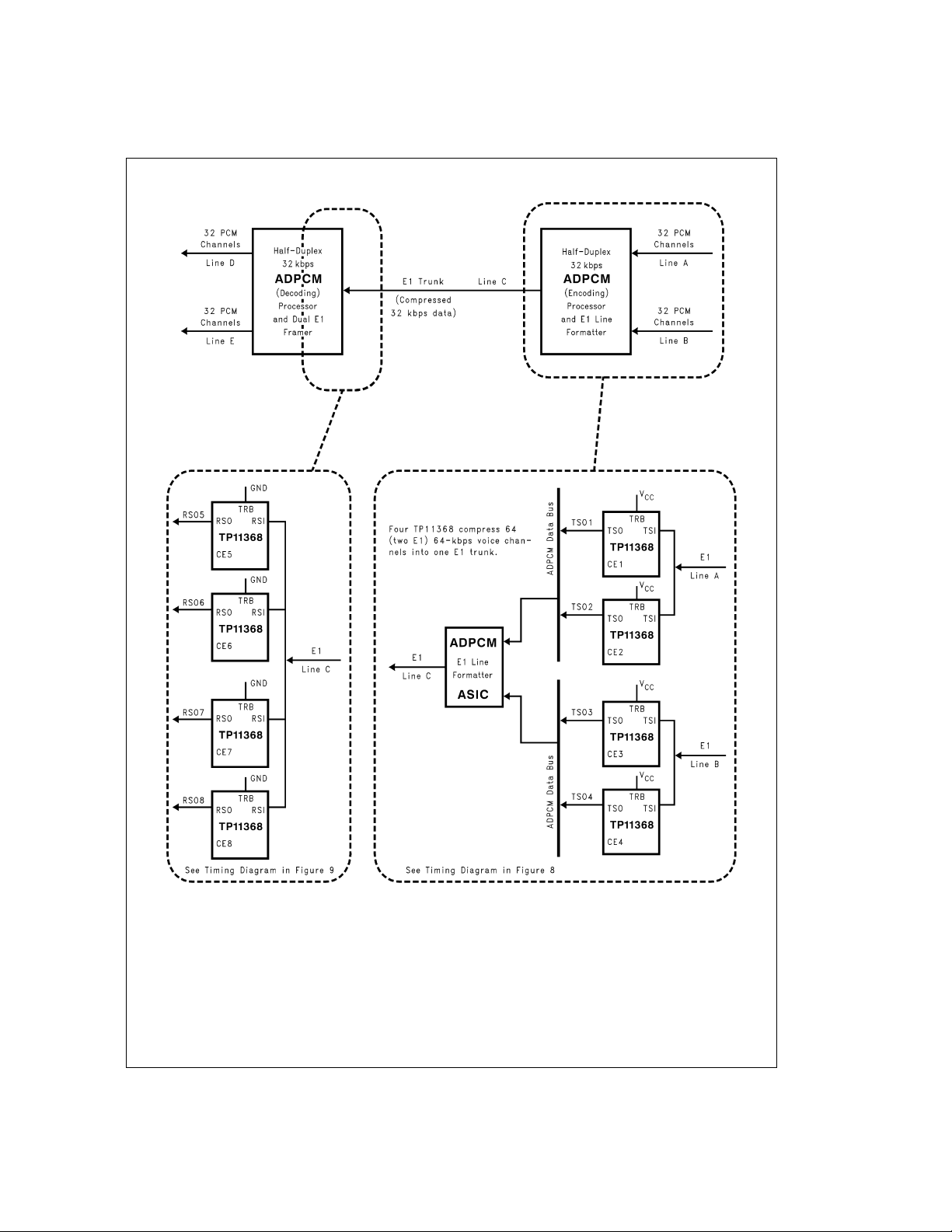
FIGURE 7. Typical Application of ADPCM Transcoders in an E1 Trunk
13 www.national.com
DS012902-9
Page 14
Applications Information (Continued)
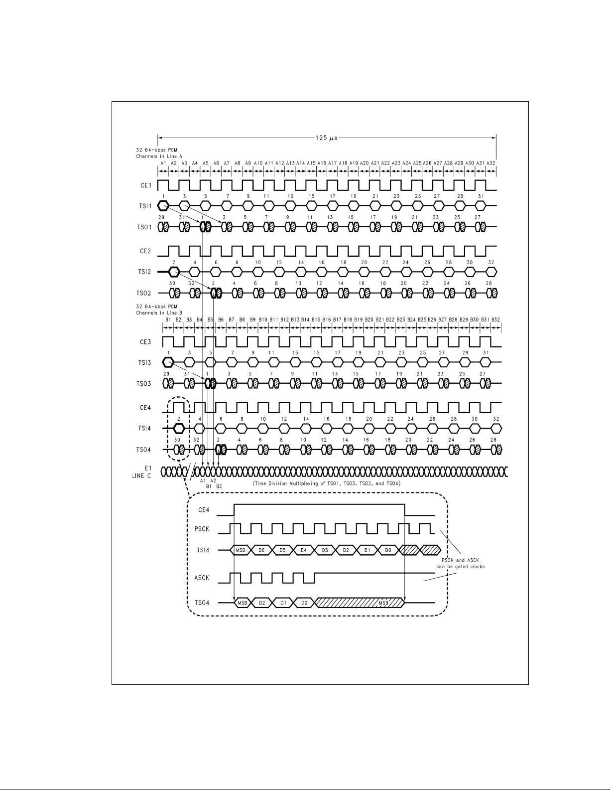
FIGURE 8. Timing Diagram of 4 TP11368 (Encoding) in an E1 Trunk Pair Gain System
www.national.com 14
DS012902-10
Page 15
Applications Information (Continued)
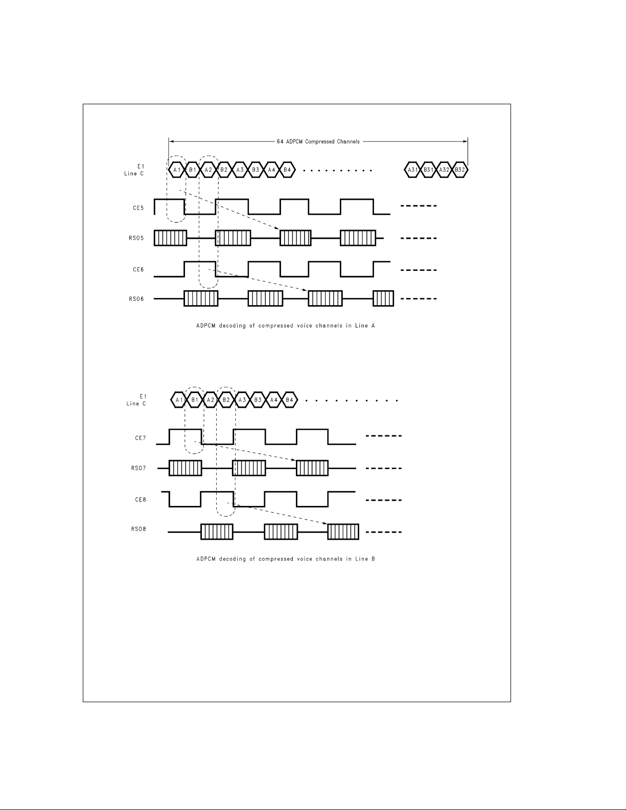
FIGURE 9. Timing Diagram of ADPCM Decoding Processor
15 www.national.com
DS012902-11
Page 16

16
Page 17
Physical Dimensions inches (millimeters) unless otherwise noted
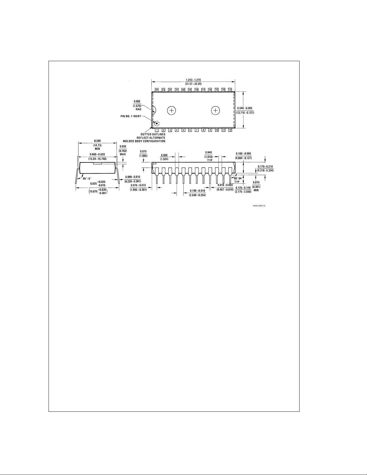
24-Lead (0.600" Wide) Molded Dual-In-Line Package
Order Number TP11368N
NS Package Number N24A
17 www.national.com
Page 18
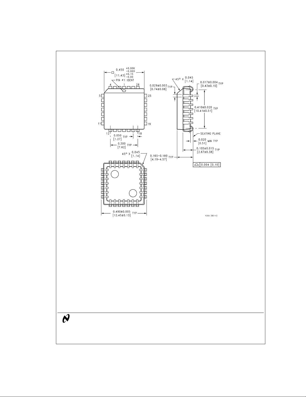
Physical Dimensions inches (millimeters) unless otherwise noted (Continued)
TP11368 Octal Adaptive Differential PCM Processor
28-Lead Molded Plastic Leaded Chip Carrier
LIFE SUPPORT POLICY
NATIONAL’S PRODUCTS ARE NOT AUTHORIZED FOR USE AS CRITICAL COMPONENTS IN LIFE SUPPORT DEVICES OR SYSTEMS WITHOUT THE EXPRESS WRITTEN APPROVAL OF THE PRESIDENT OF NATIONAL SEMICONDUCTOR CORPORATION. As used herein:
1. Life support devices or systems are devices or systems which, (a) are intended for surgical implant into
the body, or (b) support or sustain life, and whose failure to perform when properly used in accordance
with instructions for use provided in the labeling, can
be reasonably expected to result in a significant injury
to the user.
National Semiconductor
Corporation
Americas
Tel: 1-800-272-9959
Fax: 1-800-737-7018
Email: [email protected]
www.national.com
National does not assume any responsibility for use of any circuitry described, no circuit patent licenses are implied and National reserves the right at any time without notice to change said circuitry and specifications.
National Semiconductor
Europe
Deutsch Tel: +49 (0) 1 80-530 85 85
English Tel: +49 (0) 1 80-532 78 32
Français Tel: +49 (0) 1 80-532 93 58
Italiano Tel: +49 (0) 1 80-534 16 80
Order Number TP11368V
NS Package Number V28A
Fax: +49 (0) 1 80-530 85 86
Email: [email protected]
2. A critical component in any component of a life support
device or system whose failure to perform can be reasonably expected to cause the failure of the life support
device or system, or to affect its safety or effectiveness.
National Semiconductor
Hong Kong Ltd.
13th Floor, Straight Block,
Ocean Centre, 5 Canton Rd.
Tsimshatsui, Kowloon
Hong Kong
Tel: (852) 2737-1600
Fax: (852) 2736-9960
National Semiconductor
Japan Ltd.
Tel: 81-3-5620-6175
Fax: 81-3-5620-6179
 Loading...