

Page 1
TP112
100Base-TX/FX Converter
Feature
n 100Base-TX IEEE 802.3u compatible
n Full and Half duplex with Auto-negotiation
n Fully integrated adaptive equalizers
n 125MHz clock generator and clock recovery
n Include transmit waveform shaping to reduce EMI and
filter
n Include baseline wander correction
n Support one TX interface and one Fiber module
interface(ECL interface).
n Support transmit, receive/link, full duplex LED
n Single 5 Voltage supply operation
n 128-pin PQFP
Typical Application
General Description
The TP112 is a single chip media converter for
100Base-TX to 100Base-FX. The TP112 support one
100Base-TX port over CAT5 twisted pair cable and one
ECL interface to connect with fiber module to apply in
100Base-TX/FX converter application. On the
100Base-TX side, The TP112 is directly connected to
external transformers
The chip performs data recovery, clock recovery,
adaptive equalization, auto negotiation, and baseline
wander correction function. The TP112 is compliant with
the IEEE 802.3u standard.
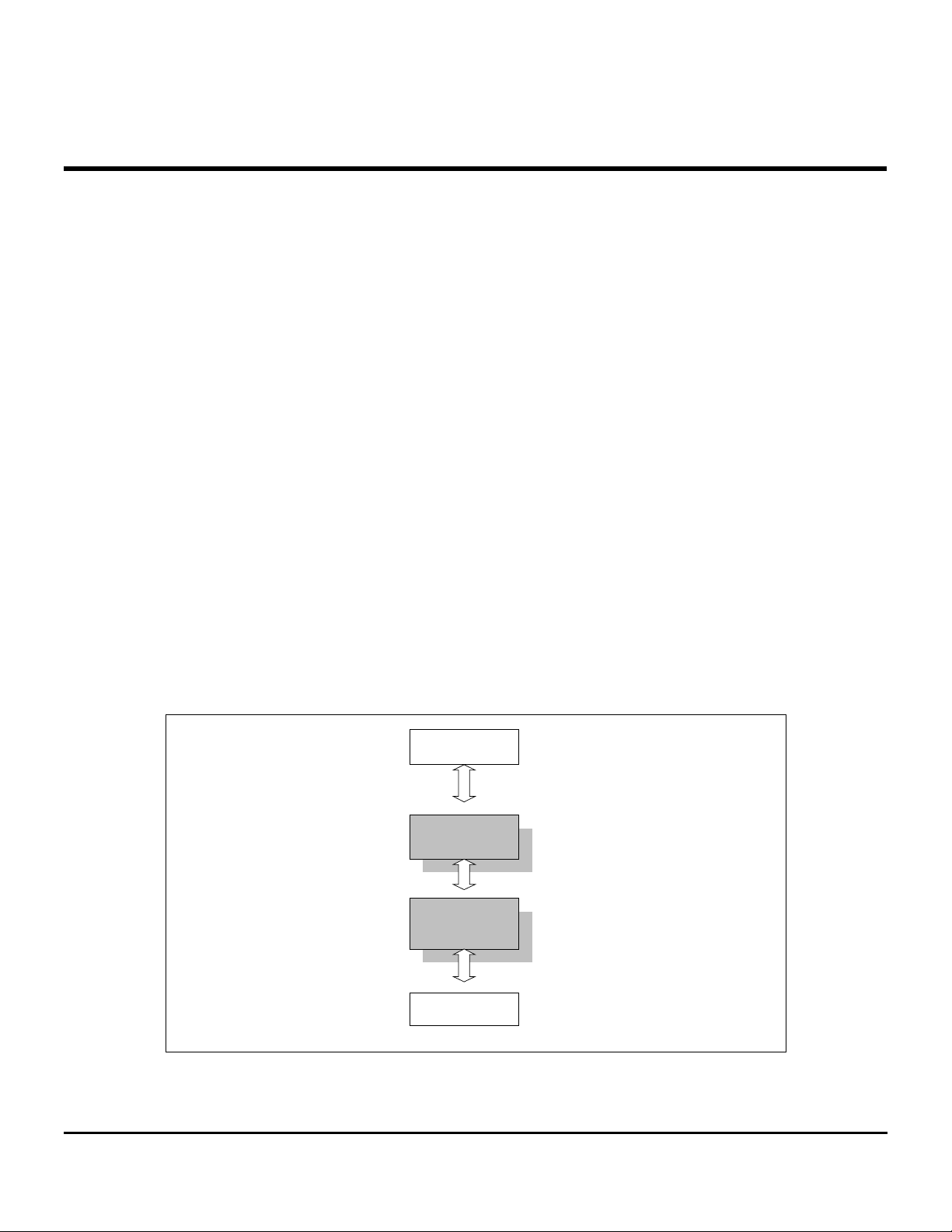
n 100Base-TX to 100Base-FX Converter
FX
Fiber Module
TP112
TX
1
TP112-DS-P02
Jan 5, 2000
Page 2
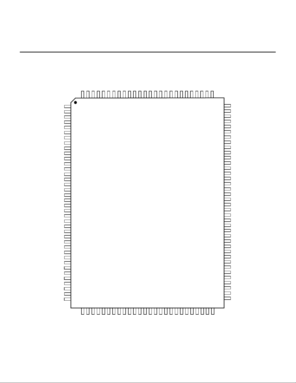
PIN Assignments
TP112
FXRDP
FXRDM
FXSD
AVCC
AVCC
NC
FXTDM
FXTDP
AGND
BGRES
BGGND
AVCC
DVCC
DGND
FORCEON
DVCC
DVCC
HALFONLY
TMODE
NC
NC
NC
DVCC
NC
DVCC
DVCC
FXTLED*
FXLRLED*
DGND
TXER1
TXD31
TXD21
TXD11
TXD01
TXCLK1
MDC
MDIO
NC
AGND
AGND
126
127
128
1
2
3
4
5
6
7
8
9
10
11
12
13
14
15
16
17
18
19
20
21
22
23
24
25
26
27
28
29
30
31
32
33
34
35
36
37
38
41
40
39
NCNCAVCC
125
42
124
43
AGND
123
44
AGND
122
45
AVCC
121
46
AGND
120
47
NC
119
AVCC
NC
AVCC
116
117
118
TP112
51
504849
AGND
115
52
AVCC
114
53
AGND
113
54
AVCC
112
55
TXOP
111
56
TXOM
110
57
AGND
109
58
AVCC
AGND
RXIM
AGND
108
107
106
105
5960616263
104
AVCC
RXIP
103
64
102
101
100
99
98
95
94
93
92
91
86
85
84
AGND
AGND
NC
NC
AVCC
97
AVCC
96
NC
NC
NC
AGND
DVCC
OSCI/X1
X2
90
DGNC
89
DVCC
88
DGND
87
DVCC
DGND
NC
DVCC
83
NC
82
NC
81
RESET*
80
TXLED*
79
LRLED*
78
DVCC
77
RXD00
76
RXD10
75
RXD20
74
RXD30
73
RXCLK0
72
DGND
71
RXER0
70
FDXLED*
69
NC
68
NC
67
NC
66
RXDV0
65
DGND
DVCC
NC
NC
DGND
RXD31
RXER1
RXDV1
RXCLK1
TXEN0
RXD01
RXD11
RXD21
TXD00
TXCLK0
TXD30
TXD20
TXD10
DVCC
TXER0
DVCC
NC
DGND
NC
DVCC
TXEN1
2
TP112-DS-P02
Jan 5, 2000
Page 3
A
PIN Description
TYPE DESCRIPTION
I Used as Input pin
O Used as Output pin
I/O Used as Input and Output pin
O Used as Output with Open Drain
PIN NO. LABEL TYPE DESCRIPTION
Media Connections
104,105 RXIP,RXIM I
111,110 TXOP,TXOM O
1,2 FXRDP,FXRDM I
8,7 FXTDP,FXTDM O
3 FXSD I
MII Interface
59
30
52
39
53
35
58,57,56,55
31,32,33,34
65
45
70
46
72
47
73,74,75,76
48,49,50,51
TXER0
TXER1
TXEN0
TXEN1
TXCLK0
TXCLK1
TXD[3:0]0
TXD[3:0]1
RXDV0
RXDV1
RXER0
RXER1
RXCLK0
RXCLK1
RXD[3:0]0
RXD[3:0]1
I/O
O3s
O
O
O
Receiver Pair
Differential data from external transformers RD± pair.
Transmit Pair
Differential data to external transformers TD± pair.
Fiber Receiver Data Pair
Used to receiver the data from the fiber transceiver module,
need external pull high resistor and pull low resistor, depend
on impedance match of the fiber transceiver module.
Fiber Transmit Data Pair
It used as output the data into the fiber transceiver module,
need external pull high resistor and pull low resistor, depend
on impedance match of the fiber transceiver module.
Fiber Signal Detect
Used as an input pin from the Fiber transceiver module to
indicate a valid signal quality had been detect.
Transmit Error
I
ctive high. When an error happened in the transmit data
stream.
Transmit Enable
I
Active high. Indicate 4B data valid on TXD[3:0]
Transmit Clock
Output is 25MHz continuous clock.
Transmit Data Input
I
4B transmit data.
Receive Data valid
Active high. Indicates that a received frame is in progress,
and data on RXD pin is valid
Receive Error
It Indicate that there's an error during a receive frame when
high
Receive Clock
25MHz output. The clock is recovered from the incoming data
on the cable inputs
Receive Data Output
4B data output and synchronously to RXCLK.
TP112
3
TP112-DS-P02
Jan 5, 2000
Page 4

PIN Description (continued)
PIN NO. LABEL TYPE DESCRIPTION
Modes
36 MDC I
37 MDIO I/O
19 TMODE I
18 HALFONLY I/IPL
15 FORCEON I/IPL
LEDs
69 FDXLED* O
78
28
79
27
Reset & Clock
80 RESET* I
91 OSCI/X1 I
90 X2 O Crystal output. Leave it unconnected (i.e., as a NC pin) when
Current Reference
10 BGRES I
11 BGGND I
LRLED*
FXLRLED*
TXLED*
FXTLED*
O
O
Management Data Clock
MII management data clock input, maximum clock rate is
2.5MHz
Management Data I/O
MII management data input/output
Test Mode
Active high. Set TP112 into test mode, and low for normal
operation. There’s an internal pull low resistor so default is
normal operation
Half Duplex Mode Only
1: half duplex
0: full duplex
Force Mode Enable
1: force mode enable
0: auto negotiation mode enable
Full Duplex LED
Before link OK, this pin is tri-stated. After link OK this pin
indicate current duplex operation for TP112. High for half
duplex and low for full duplex
Link/Receive LED
Active low. Indicates the link status of the port, driven low
when link to the port is good. Output for 20mS clock while the
TP112 is receiving data from external media
Transmit LED
Active low. Indicates that data is being transmitting
Reset
Active low. Reset TP112, remain low at least 1us.
Oscillator input or crystal input
(25MHz±50ppm).
oscillator is used.
Band Gap Resistor
A 6.2KOhm 1% resistor that supply 200uA reference current
for receive
Band Gap Resistor Ground
Band gap resistor ground reference input
TP112
4
TP112-DS-P02
Jan 5, 2000
Page 5

PIN Description (continued)
PIN NO. LABEL TYPE DESCRIPTION
Power & Ground
4,5,12,97,98,
103,108,112,
114,117,116
121,126
9,93,101,102,
106,107,109,
113,115,120,
122,123,127,
128
13,16,17,23,
25,26,41,43,
61,62,77,83,
86,88,92,
14,29,
42,54,63,71,
85,87,89
6,20,21,22,24,
38,40,44,60,64,
66,67,68,81,82,
84,94,95,96,
99,100,118,119,
124,125
AVCC I
AGND I
DVCC I
DGND I
NC
Analog VCC
+5V
Analog Ground
0V
Digital VCC
+5V
Digital Ground
0V
No Connection
TP112
5
TP112-DS-P02
Jan 5, 2000
Page 6

Absolute Maximum Rating
TP112
Supply Voltage ....................... VCC –0.25 to VDD +0.25V
Storage Temperature ....................................-65 to 150°C
Ambient Operating Temperature (Ta)................. 0 to 70°C
Stresses above those listed under Absolute Maximum
Ratings may cause permanent damage to the device.
Functional operation under these conditions is not
implied. Exposure to Absolute Maximum Rating
conditions for extended periods may affect product
reliability.
Electrical
n Operating Conditions
Parameter Sym. Min. Typ. Max. Unit Conditions
AVCC 4.75 5 5.25 V Supply Voltage
DVCC 4.75 5 5.25 V VCC=5.0V
Power Consumption ICC TBD W
n Input Clock
Parameter Sym. Min. Typ. Max. Unit Conditions
Frequency 25 MHz
Frequency Tolerance -50 +50 PPM
n I/O Electrical Characteristics
Parameter Sym. Min. Typ. Max. Unit Conditions
Input Low Voltage I VIL 0.8 V
Input High Voltage I VIH 2.0 V
Output Low Voltage O VOL 0.4 V IOH=4mA, VCC=5.0V
Output High voltage O VOH 2.4 V IOL=4mA, VCC=5.0V
n TX Transceiver Electrical Characteristics
Parameter Sym. Min. Typ. Max. Unit Conditions
Transmitter
Peak Differential Output Voltage VP 0.95 1.0 1.05 V
Signal Amplitude Symmetry - 98 100 102 %
Signal Rise/Fall Time TRF 3 4 5 ns
Rise/Fall Time Symmetry TRFS 0.5 ns
Duty Cycle Distortion - 0.5 ns
Overshoot VO 5 %
6
TP112-DS-P02
Jan 5, 2000
Page 7

Order Information
TP112
Part No. PIN Notice
TP112 128 PIN PQFP -
7
TP112-DS-P02
Jan 5, 2000
Page 8

Package Detail
QFP 128L Outline Dimensions
TP112
H
D
128
1
38
39
c
L
1
D
e
b
103
102
E
E
H
65
64
GAGE
2
A
1
A
y
D
PLANE
L
Unit: Inches/mm
Dimensions In Inches Dimensions In mm Symbol
Min. Nom. Max. Min. Nom. Max.
A1 0.010 0.014 0.018 0.25 0.35 0.45
A2 0.107 0.112 0.117 2.73 2.85 2.97
b
c
HD 0.669 0.677 0.685 17.00 17.20 17.40
D 0.547 0.551 0.555 13.90 14.00 14.10
HE 0.906 0.913 0.921 23.00 23.20 23.40
E 0.783 0.787 0.791 19.90 20.00 20.10
e - 0.020 - - 0.50 -
L 0.025 0.035 0.041 0.65 0.88 1.03
L1
y - - 0.004 - - 0.10
θ 0°
0.007 0.009 0.011 0.17 0.22 0.27
0.004 0.006 0.008 0.09 0.15 0.20
- 0.063 - - 1.60 -
-
12° 0°
-
12°
Note:
1. Dimension D & E do not include mold protrusion.
2. Dimension B does not include dambar protrusion.
Total in excess of the B dimension at maximum material condition.
Dambar cannot be located on the lower radius of the foot.
8
TP112-DS-P02
Jan 5, 2000
 Loading...