

Page 1
®
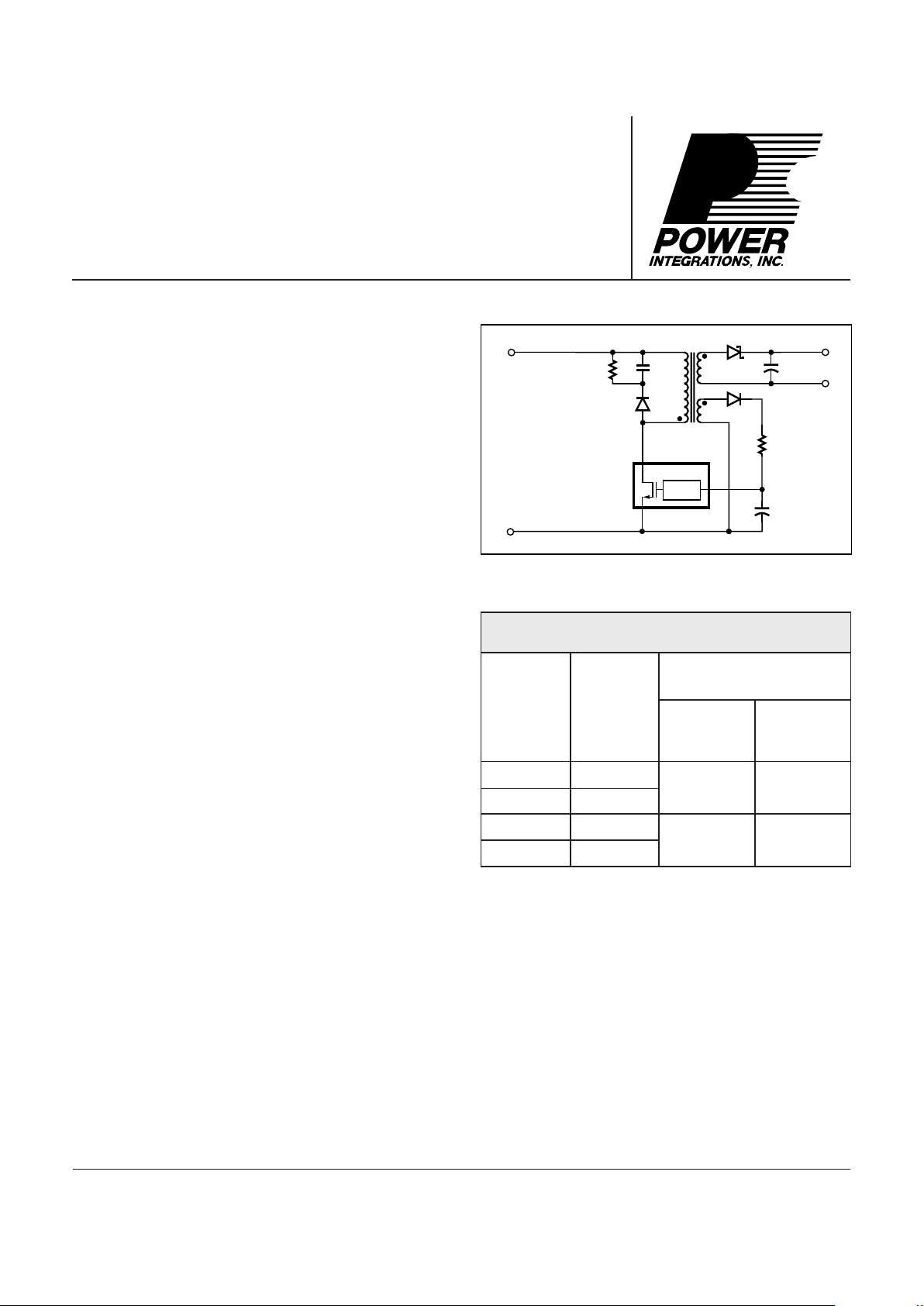
Figure 1. Typical Application.
TOP209/210
TOPSwitch
Family
Three-terminal Off-line PWM Switch
ORDER
PART
NUMBER
OUTPUT POWER RANGE
®
85-265
VAC
230 VAC or
110 VAC
w/Doubler
PI-2043-052397
Wide-Range
DC Input
D
S
C
CONTROL
TOPSwitch
+
-
Product Highlights
Cost Effective Switcher for Low Power Applications
• Replaces linear power supplies
• Replaces discrete switcher and 20 to 50 components
– cuts cost, increases reliability
• Stand-by power supplies for Green or energy efficient
products such as personal computers, monitors, UPS,
copiers, fax machines, etc.
• Housekeeping or "keep-alive" power supply applications
such as TV, appliances, industrial control and personal
computers
• Meets 'Blue Angel' low power stand-by specification
• Controlled MOSFET turn-on reduces EMI and EMI filter
costs
• 80% smaller and lighter compared to linear supply
• 50% smaller compared to discrete switcher
Over 80% Efficiency in Flyback Topology
• Built-in start-up and current limit reduce DC losses
• Low capacitance 700 V MOSFET cuts AC losses
• CMOS controller/gate driver consumes only 6 mW
• 70% maximum duty cycle minimizes conduction losses
Simplifies Design – Reduces Time to Market
• Supported by reference design boards
• Integrated PWM Controller and 700 V MOSFET in
industry standard eight pin DIP package
• Only one external capacitor needed for compensation,
bypass and start-up/auto-restart functions
• Easily interfaces with both opto and primary feedback
System Level Fault Protection Features
• Auto-restart and cycle by cycle current limiting functions
handle both primary and secondary faults
• On-chip thermal shutdown with hysteresis protects the
entire system against overload
Description
The TOP209/210 implements all functions necessary for an
off-line switched mode control system: high voltage N-channel
power MOSFET with controlled turn-on gate driver, voltage
mode PWM controller with integrated oscillator, high voltage
start-up bias circuit, bandgap derived reference, bias shunt
regulator/error amplifier for loop compensation and fault
protection circuitry. Compared to discrete MOSFET and
controller or self oscillating (RCC) switching converter
solutions, a TOPSwitch integrated circuit can reduce total cost,
component count, size, weight and at the same time increase
efficiency and system reliability. The TOP209/210 are intended
for 100/110/230 VAC off-line Power Supply applications in
the 0 to 8 W (0 to 5 W universal) range.
TOP209P
TOP210PFI
TOPSwitch
Selection Guide
PACKAGE
DIP-8
TOP209G
TOP210G
0-4 W
0-2 W
0-8 W
0-5 W
DIP-8
SMD-8
SMD-8
August 1997
Page 2
A
8/97
2
TOP209/210
2
PI-1742-011796
SHUTDOWN/
AUTO-RESTART
PWM
COMPARATOR
CLOCK
SAW
OSCILLATOR
CONTROLLED
TURN-ON
GATE
DRIVER
INTERNAL
SUPPLY
5.7 V
4.7 V
SOURCE
SRQ
Q
D
MAX
+
CONTROL
+
5.7 V
I
FB
R
E
Z
C
V
C
MINIMUM
ON-TIME
DELAY
+
-
V
I
LIMIT
LEADING
EDGE
BLANKING
POWER-UP
RESET
÷ 8
0
1
THERMAL
SHUTDOWN
WITH
HYSTERESIS
SHUNT REGULATOR/
ERROR AMPLIFIER
+
-
DRAIN
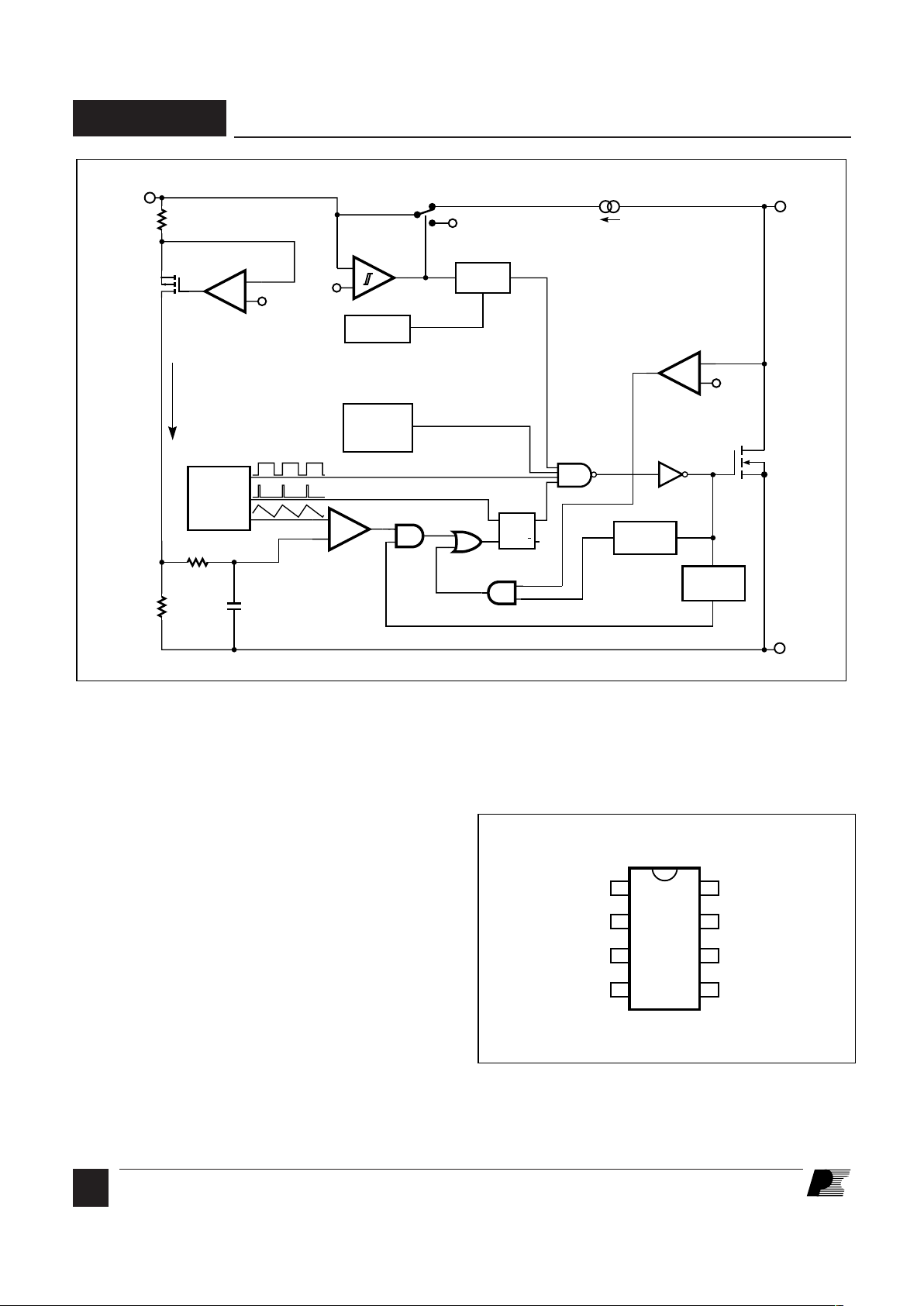
Figure 2. Functional Block Diagram.
Pin Functional Description
DRAIN Pin:
Output MOSFET drain connection. Provides internal bias
current during start-up operation via an internal switched highvoltage current source. Internal current sense point.
CONTROL Pin:
Error amplifier and feedback current input pin for duty cycle
control. Internal shunt regulator connection to provide internal
bias current during normal operation. It is also used as the
supply bypass and auto-restart/compensation capacitor
connection point.
SOURCE Pin:
Control circuit common, internally connected to output
MOSFET source.
SOURCE (HV RTN) Pin:
Output MOSFET source connection for high voltage return.
PI—2044-040901
CONTROL
8
5
7
6
DRAIN
N/C
N/C
N/C
1
4
2
3
N/C
SOURCE (HV RTN)
SOURCE
P Package (DIP-8)
G Package (SMD-8)
Figure 3. Pin Configuration.
Page 3
A
8/97
TOP209/210
3
TOPSwitch
Family Functional Description
TOPSwitch is a self biased and protected
linear control current-to-duty cycle
converter with an open drain output.
High efficiency is achieved through the
use of CMOS and integration of the
maximum number of functions possible.
CMOS significantly reduces bias
currents as compared to bipolar or
discrete solutions. Integration eliminates
external power resistors used for current
sensing and/or supplying initial start-up
bias current.
During normal operation, the internal
output MOSFET duty cycle linearly
decreases with increasing CONTROL
pin current as shown in Figure 4. To
implement all the required control, bias,
and protection functions, the DRAIN
and CONTROL pins each perform
several functions as described below.
Refer to Figure 2 for a block diagram
and Figure 6 for timing and voltage
waveforms of the TOPSwitch integrated
circuit.
Control Voltage Supply
CONTROL pin voltage VC is the supply
or bias voltage for the controller and
driver circuitry. An external bypass
capacitor closely connected between the
CONTROL and SOURCE pins is
required to supply the gate drive current.
The total amount of capacitance
connected to this pin (CT) also sets the
auto-restart timing as well as control
loop compensation. VC is regulated in
either of two modes of operation.
Hysteretic regulation is used for initial
start-up and overload operation. Shunt
regulation is used to separate the duty
cycle error signal from the control circuit
supply current. During start-up, V
C
current is supplied from a high-voltage
switched current source connected
internally between the DRAIN and
CONTROL pins. The current source
provides sufficient current to supply the
control circuitry as well as charge the
total external capacitance (CT).
PI-2047-060497
D
MAX
D
MIN
I
CD1
Duty Cycle (%)
IC (mA)
2.5 6.5
Slope = PWM Gain
-16%/mA
I
B
Auto-restart
Figure 4. Relationship of Duty Cycle to CONTROL Pin Current.
Figure 5. Start-up Waveforms for (a) Normal Operation and (b) Auto-restart.
DRAIN
0
V
IN
V
C
0
4.7 V
5.7 V
8 Cycles
95%
5%
Off
Switching Switching
Off
I
C
Charging C
T
I
CD1
Discharging C
T
I
CD2
Discharging C
T
I
C
Charging C
T
Off
PI-1124A-060694
DRAIN
0
V
IN
V
C
0
4.7 V
5.7 V
Off
Switching
(b)
(a)
CT is the total external capacitance
connected to the CONTROL pin
Page 4

A
8/97
4
TOP209/210
2
The first time VC reaches the upper threshold, the high-voltage
current source is turned off and the PWM modulator and output
transistor are activated, as shown in Figure 5(a). During normal
operation (when the output voltage is regulated) feedback
control current supplies the V
C
supply current. The shunt
regulator keeps VC at typically 5.7 V by shunting CONTROL
pin feedback current exceeding the required DC supply current
through the PWM error signal sense resistor RE. The low
dynamic impedance of this pin (ZC) sets the gain of the error
amplifier when used in a primary feedback configuration. The
dynamic impedance of the CONTROL pin together with the
external resistance and capacitance determines the control loop
compensation of the power system.
If the CONTROL pin external capacitance (CT) should discharge
to the lower threshold, then the output MOSFET is turned off
and the control circuit is placed in a low-current standby mode.
The high-voltage current source is turned on and charges the
external capacitance again. Charging current is shown with a
negative polarity and discharging current is shown with a
positive polarity in Figure 6. The hysteretic auto-restart
comparator keeps VC within a window of typically 4.7 to 5.7 V
by turning the high-voltage current source on and off as shown
in Figure 5(b). The auto-restart circuit has a divide-by-8
counter which prevents the output MOSFET from turning on
again until eight discharge-charge cycles have elapsed. The
counter effectively limits TOPSwitch power dissipation by
reducing the auto-restart duty cycle to typically 5%. Autorestart continues to cycle until output voltage regulation is
again achieved.
Bandgap Reference
All critical TOPSwitch internal voltages are derived from a
temperature-compensated bandgap reference. This reference
is also used to generate a temperature-compensated current
source which is trimmed to accurately set the oscillator frequency
and MOSFET gate drive current.
Oscillator
The internal oscillator linearly charges and discharges the
internal capacitance between two voltage levels to create a
sawtooth waveform for the pulse width modulator. The oscillator
sets the pulse width modulator/current limit latch at the beginning
of each cycle. The nominal frequency of 100 kHz was chosen
to minimize EMI and maximize efficiency in power supply
applications. Trimming of the current reference improves
oscillator frequency accuracy.
Pulse Width Modulator
The pulse width modulator implements a voltage-mode control
loop by driving the output MOSFET with a duty cycle inversely
proportional to the current flowing into the CONTROL pin.
The error signal across R
E
is filtered by an RC network with a
typical corner frequency of 7 kHz to reduce the effect of
switching noise. The filtered error signal is compared with the
internal oscillator sawtooth waveform to generate the duty
cycle waveform. As the control current increases, the duty
cycle decreases. A clock signal from the oscillator sets a latch
which turns on the output MOSFET. The pulse width modulator
resets the latch, turning off the output MOSFET. The maximum
duty cycle is set by the symmetry of the internal oscillator. The
modulator has a minimum ON-time to keep the current
consumption of the TOPSwitch independent of the error signal.
Note that a minimum current must be driven into the CONTROL
pin before the duty cycle begins to change.
Gate Driver
The gate driver is designed to turn the output MOSFET on at a
controlled rate to minimize common-mode EMI. The gate drive
current is trimmed for improved accuracy.
Error Amplifier
The shunt regulator can also perform the function of an error
amplifier in primary feedback applications. The shunt regulator
voltage is accurately derived from the temperature compensated
bandgap reference. The gain of the error amplifier is set by the
CONTROL pin dynamic impedance. The CONTROL pin
clamps external circuit signals to the V
C
voltage level. The
CONTROL pin current in excess of the supply current is
separated by the shunt regulator and flows through RE as the
error signal.
Cycle-By-Cycle Current Limit
The cycle by cycle peak drain current limit circuit uses the
output MOSFET ON-resistance as a sense resistor. A current
limit comparator compares the output MOSFET ON-state drainsource voltage, V
DS(ON)
, with a threshold voltage. High drain
current causes V
DS(ON)
to exceed the threshold voltage and turns
the output MOSFET off until the start of the next clock cycle.
The current limit comparator threshold voltage is temperature
compensated to minimize variation of the effective peak current
limit due to temperature related changes in output MOSFET
R
DS(ON)
.
The leading edge blanking circuit inhibits the current limit
comparator for a short time after the output MOSFET is turned
on. The leading edge blanking time has been set so that current
spikes caused by primary-side capacitances and secondary-side
rectifier reverse recovery time will not cause premature
termination of the switching pulse.
TOPSwitch
Family Functional Description (cont.)
Page 5
A
8/97
TOP209/210
5
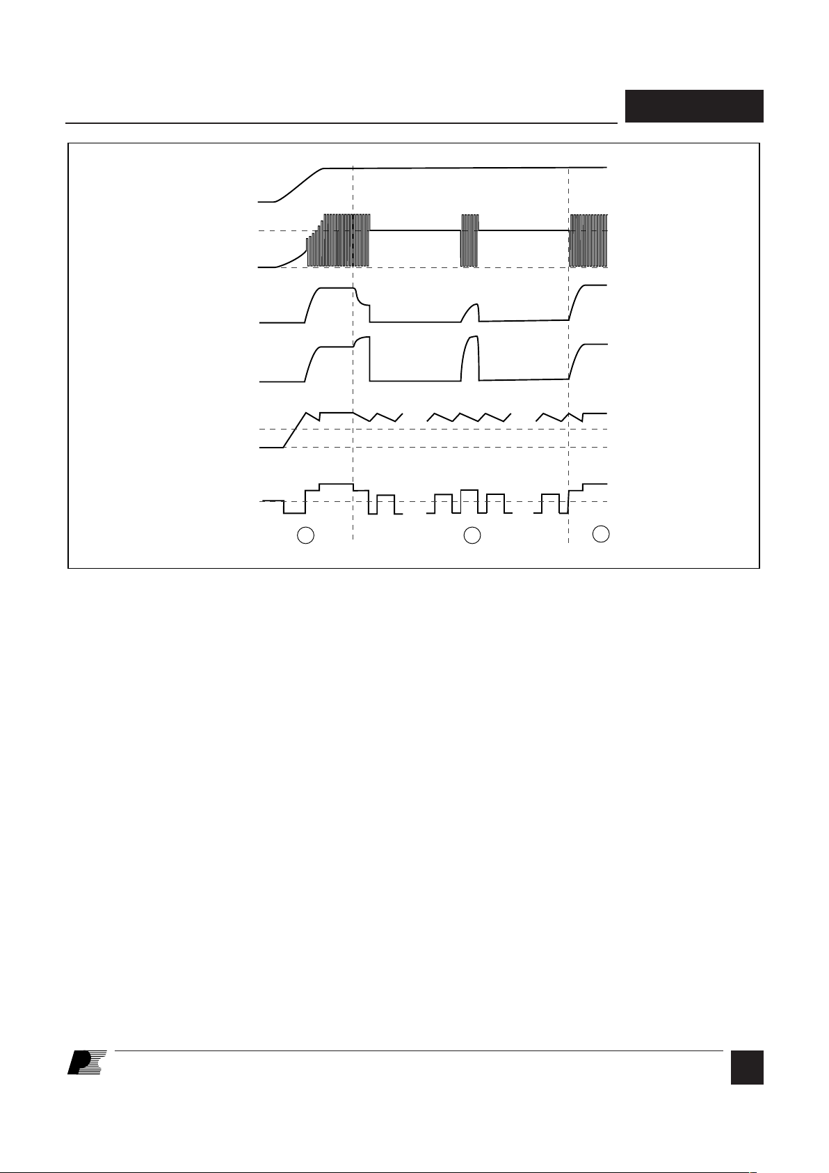
PI-1742-011796
V
IN
V
OUT
0
I
OUT
0
1 2
1
DRAIN
0
V
IN
V
C
0
••• •••
12 12 81
0
I
C
••• •••
12
8
812 81
Shutdown/Auto-restart
To minimize TOPSwitch power dissipation, the shutdown/
auto-restart circuit turns the power supply on and off at a duty
cycle of typically 5% if an out of regulation condition persists.
Loss of regulation interrupts the external current into the
CONTROL pin. VC regulation changes from shunt mode to the
hysteretic auto-restart mode described above. When the fault
condition is removed, the power supply output becomes
regulated, VC regulation returns to shunt mode, and normal
operation of the power supply resumes.
Hysteretic Overtemperature Protection
Temperature protection is provided by a precision analog
circuit that turns the output MOSFET off when the junction
temperature exceeds the thermal shutdown temperature
(typically 145 °C). When the junction temperature cools past
the hysteresis temperature, normal operation resumes. VC is
regulated in hysteretic mode while the power supply is turned
off.
High-voltage Bias Current Source
This current source biases TOPSwitch from the DRAIN pin and
charges the CONTROL pin external capacitance (CT) during
start-up or hysteretic operation. The current source is switched
on and off with an effective duty cycle of approximately 35%.
This duty cycle is determined by the ratio of CONTROL pin
charge (IC) and discharge currents (I
CD1
and I
CD2
). This current
source is turned off during normal operation when the output
MOSFET is switching.
Figure 6. Typical Waveforms for (1) Normal Operation, (2) Auto-restart.
Page 6

A
8/97
6
TOP209/210
2
General Circuit Description
Figure 7 shows a low-cost, DC input, flyback switching power
supply using the TOP210 integrated circuit. This 5 V, 4 W
power supply operates from a DC voltage derived from rectified
and filtered AC mains voltage of 85 to 265 VAC. The 5 V
output is indirectly sensed via the primary bias winding. The
output voltage is determined by the TOPSwitch CONTROL pin
shunt regulator voltage (V
C
), the voltage drops of rectifiers D2
and D3, and the turns ratio between the bias winding and output
winding of T1. Other output voltages are also possible by
adjusting the transformer turns ratios.
The high voltage DC bus is applied to the primary winding of
T1. Capacitor C1 filters the high voltage supply, and is only
necessary if the connections between the high voltage DC
supply and the TOP210 are long. The other side of the
transformer primary is driven by the integrated high-voltage
MOSFET within the TOP210. D1 and VR1 clamp the voltage
spike caused by transformer leakage inductance to a safe value
and reduce ringing at the DRAIN of U1. The power secondary
winding is rectified and filtered by D2, C2, L1, and C3 to create
the 5V output voltage. The bias winding is rectified and filtered
by D3, R1 and C5 to create a bias voltage to the TOP210. C5
also filters internal MOSFET gate drive charge current spikes
on the CONTROL pin, determines the auto-restart frequency,
and together with R1, compensates the control loop.
PI-2045-041798
+5 V
RTN
C1
10 nF
400 V
C5
47 µF
10 V
D2
1N5822
D3
1N4148
C2
330 µF
10 V
T1
D1
UF4005
C3
100 µF
10 V
R1
15 Ω
VR1
BZY97-
C120
120 V
L1
3.3 µH
CIRCUIT PERFORMANCE:
Line Regulation - –1.5%
(104-370 VDC)
Load Regulation - –5%
(10-100%)
Ripple Voltage –25 mV
+
-
U1
TOP210
2
1
3
4
5
8
DC
INPUT
TRD1
D
S
C
CONTROL
TOPSwitch
Figure 7. Schematic Diagram of a Minimum Parts Count 5 V, 4 W Bias Supply Using the TOP210.
Page 7

A
8/97
TOP209/210
7
Figure 8. Schematic Diagram of a 12 V, 8 W 110/220 VAC Input Power Supply Using the TOP210.
The circuit shown in Figure 8 produces a 12 V, 8 W power
supply that operates from 85 to 132 VAC or 170 to 264 VAC
input voltage. The 12 V output voltage is determined by the
TOPSwitch CONTROL pin shunt regulator voltage, the voltage
drops of D2 and D3, and the turns ratio between the bias and
output windings of T1. Other output voltages are also possible
by adjusting the transformer turns ratios. R1 and C5 provide
filtering of the bias winding to improve line and load regulation.
AC power is rectified and filtered by BR1, C1 and C9 to create
the high voltage DC bus applied to the primary winding of T1.
The other side of the transformer primary is driven by the
integrated high-voltage MOSFET within the TOP210. JP1 is a
jumper used to select 110 VAC or 220 VAC operation. Installing
JP1 selects 110 VAC operation. Leaving JP1 open selects
220 VAC operation. RA and RB, which equalize voltage across
C1 and C9, are necessary only when JP1 is not installed. D1 and
VR1 clamp the leading-edge voltage spike caused by transformer
leakage inductance to a safe value and reduce ringing. The
power secondary winding is rectified and filtered by D2, C2,
L1, and C3 to create the 12 V output voltage. R2 provides a preload on the 12 V output to improve load regulation at light loads.
The bias winding is rectified and filtered by D3, R1, and C5 to
create a bias voltage to the TOP210. L2 and Y1-capacitor C7
attenuate common-mode emission currents caused by highvoltage switching waveforms on the DRAIN side of the primary
winding and the primary to secondary capacitance. L2 and C6
attenuate differential-mode emission currents caused by the
fundamental and harmonics of the trapezoidal primary current
waveform. C5 filters internal MOSFET gate drive charge
current spikes on the CONTROL pin, determines the autorestart frequency, and together with R1, compensates the control
loop.
PI-2046-052397
VR1
BZY97-C200
D1
UF4005
R1
6.8 Ω
3 µH
RA
470 kΩ
RB
470 kΩ
JP1*
JUMPER
BR1
DFO6M
C1
10 µF
200 V
R2
330
1W
L1
F1
2A
T1
T1RD2
1
4
+
-
2
3
8
D2
MBR360
5
L2
12 mH min.
0.2A
C6
47nF
250VAC
X2
C7
1nF
250 VAC
Y1
* JPI INSTALLED FOR 110 VAC INPUT
JPI OPEN FOR 220 VAC INPUT
C5
47 µF
10 V
D3
1N4148
C3
120 µF
16 V
C2
330 µF
16 V
C9
10 µF
200 V
12 V
RTN
CIRCUIT PERFORMANCE:
Line Regulation - –1%
(85-132 VAC) or
(170-265 VAC)
Load Regulation - –5%
(10-100%)
Ripple Voltage – 50 mV
Meets CISPR-22 Class B
J1
L
N
U1
TOP210
D
S
C
CONTROL
TOPSwitch
Page 8

A
8/97
8
TOP209/210
2
Figure 9. Recommended PC Layout for the TOP209/210.
CONTROL
SOURCE
SOURCE
DRAIN
TOP VIEW
PI-1744-011796
High Voltage
Return
Bias/Feedback
Return
Bypass
Capacitor
Bias/Feedback
Input
TOP210 PFI
Use a Kelvin connection to the SOURCE pin for the CONTROL
pin bypass capacitor as shown in Figure 9.
Minimize peak voltage and ringing on the DRAIN voltage at
turn-off. Use a Zener or TVS Zener diode to clamp the DRAIN
voltage.
Under some conditions, externally provided bias or supply
current driven into the CONTROL pin can hold the TOPSwitch
in one of the 8 auto-restart cycles indefinitely and prevent
starting. Shorting the CONTROL pin to the SOURCE pin will
reset the TOPSwitch. To avoid this problem when doing bench
evaluations, it is recommended that the V
C
power supply be
turned on before the DRAIN voltage is applied.
Key Application Considerations
CONTROL pin currents during auto-restart operation are much
lower at low input voltages (< 20 V) which increases the autorestart cycle period (see the IC vs. Drain Voltage Characteristic
curve).
Short interruptions of AC power may cause TOPSwitch to enter
the 8-count auto-restart cycle before starting again. This is
because the input energy storage capacitors are not completely
discharged and the CONTROL pin capacitance has not
discharged below the internal power-up reset voltage (V
C(RESET)
).
In some cases, minimum loading may be necessary to keep a
lightly loaded or unloaded output voltage within the desired
range due to the minimum ON-time.
For additional applications information regarding the TOPSwitch
family, refer to AN-14 in the 1996-97 Data Book and Design
Guide or on our Web site.
Page 9

A
8/97
TOP209/210
9
ABSOLUTE MAXIMUM RATINGS
(1)
DRAIN Voltage ........................................... - 0.3 to 700 V
CONTROL Voltage ..................................... - 0.3 V to 9 V
CONTROL Current ...............................................100 mA
1. Unless noted, all voltages referenced to SOURCE,
TA = 25 °C.
Storage Temperature ..................................... -65 to 150 °C
Operating Junction Temperature
(2)
................-40 to 150 °C
Lead Temperature
(3)
................................................ 260 °C
Thermal Impedance (θJA) ................................... 100 °C/W
Thermal Impedance (θJC) ..................................... 40 °C/W
2. Normally limited by internal circuitry.
3. 1/16" from case for 5 seconds.
f
OSC
D
MAX
D
MIN
I
B
Z
C
I
C
V
C(AR)
CONTROL FUNCTIONS
Output
Frequency
Maximum
Duty Cycle
Minimum
Duty Cycle
PWM
Gain
PWM Gain
Temperature Drift
External
Bias Current
Dynamic
Impedance
Dynamic Impedance
Temperature Drift
CONTROL Pin
Charging Current
Charging Current
Temperature Drift
Auto-restart
Threshold Voltage
kHz
%
%
%/mA
%/mA/°C
mA
Ω
%/°C
mA
%/°C
V
SHUTDOWN/AUTO-RESTART
Conditions
(Unless Otherwise Specified)
Parameter Symbol See Figure 12 Units
SOURCE = 0 V
T
J
= -40 to 125 °C
Min Typ Max
TOP209
TOP210
TOP209
TOP210
IC = 4 mA, TJ = 25 °C
IC = I
CD1
+ 0.5 mA, See Figure 10
IC = 10 mA
See Figure 10
IC = 4 mA, TJ = 25 °C
See Figure 4
See Note A
See Figure 4
IC = 4 mA, TJ = 25 °C
See Figure 11
VC = 0 V
TJ = 25 °C
VC = 5 V
See Note A
S1 open
55 70 85
90 100 110
64 67 70
0.5 1.5 2.5
1.0 1.8 3.0
-11 -16 -21
-0.05
1.5 2.5 4
10 15 22
0.18
-2.4 -1.9 -1.2
-2 -1.5 -0.8
0.4
5.7
Page 10

A
8/97
10
TOP209/210
2
4.4 4.7 5.0
0.6 1.0
59
1.2
0.150 0.230
0.230 0.300
150
100
125 145
30
2.0 3.3 4.2
S1 open
S1 open
S1 open
S1 open
di/dt = 40 mA/µs, TJ = 25 °C
IC = 4 mA
IC = 4 mA
IC = 4 mA
S2 open
I
LIMIT
t
LEB
t
ILD
V
C(RESET)
V
V
%
Hz
A
ns
ns
°C
°C
V
SHUTDOWN/AUTO-RESTART (cont.)
UV Lockout
Threshold Voltage
Auto-restart
Hysteresis Voltage
Auto-restart
Duty Cycle
Auto-restart
Frequency
Self-protection
Current Limit
Leading Edge
Blanking Time
Current Limit
Delay
Thermal Shutdown
Temperature
Thermal Shutdown
Hysteresis
Power-up Reset
Threshold Voltage
CIRCUIT PROTECTION
Conditions
(Unless Otherwise Specified)
Parameter Symbol See Figure 12 Units
SOURCE = 0 V
TJ = -40 to 125 °C
Min Typ Max
TOP209
TOP210
Page 11

A
8/97
TOP209/210
11
31.2 36.0
51.4 59.4
250
700
100
50
36
5.5 5.8 6.1
±50
0.6 1.2 1.6
0.5 0.8 1.1
ON-State
Resistance
OFF-State
Current
Breakdown
Voltage
Rise
Time
Fall
Time
DRAIN Supply
Voltage
Shunt Regulator
Voltage
Shunt Regulator
Temperature Drift
CONTROL Supply/
Discharge Current
OUTPUT
SUPPLY
TJ = 25 °C
TJ = 100 °C
See Note B, ID = 100 µA, TA = 25 °C
See Note C
IC = 4 mA
Output MOSFET Enabled
Output MOSFET Disabled
Conditions
(Unless Otherwise Specified)
Parameter Symbol See Figure 12 Units
SOURCE = 0 V
T
J
= -40 to 125 °C
Min Typ Max
Ω
µA
V
ns
ns
V
V
ppm/°C
mA
R
DS(ON)
I
DSS
BV
DSS
t
R
t
F
V
C(SHUNT)
I
CD1
I
CD2
NOTES:
A. For specifications with negative values, a negative temperature coefficient corresponds to an increase in magnitude
with increasing temperature, and a positive temperature coefficient corresponds to a decrease in magnitude with
increasing temperature.
B. The breakdown & leakage measurements can be accomplished by using the TOPSwitch auto-restart feature. The
divide-by-8 counter in the auto-restart circuitry disables the output MOSFET from switching in 7 out of 8 cycles. To
place the TOPSwitch in one of these cycles, the following procedure can be carried out using the modified circuit of
Figure 12:
Measured
in a Typical
Flyback Converter Application
ID = 25 mA
See Note B
VDS = 560 V, TA = 125 °C
Page 12

A
8/97
12
TOP209/210
2
NOTES: (continued)
i. The 470 Ω 5 W load resistor at the DRAIN pin should be shorted. S1 & S2 should stay closed.
ii. The 40 V output supply should be replaced with a curve tracer capable of forcing 700 V.
iii. The curve tracer should initially be set at 0 V. The 0-50 V variable supply should be adjusted through a voltage
sequence of 0 V, 6.5 V, 4.2 V, and 6.5 V.
iv. The breakdown and the leakage measurements can now be taken with the curve tracer. The maximum
voltage from the curve tracer must be limited to 700 V under all conditions.
C.It is possible to start up and operate TOPSwitch at DRAIN voltages well below 36 V. However, the CONTROL pin
charging current is reduced, which affects start-up time and auto-restart frequency and duty cycle. Refer to the
characteristic graph on CONTROL pin charge current (I
C
) vs. DRAIN voltage for low voltage operation characteristics.
PI-1733-122095
0.1 µF
47 µF 0-50 V
40 V
470 Ω
5 W
S2
S1
470 Ω
NOTE: This test circuit is not applicable for current limit or output characteristic measurements.
DC
SS
Figure 12. TOPSwitch General Test Circuit.
Figure 10. TOPSwitch Duty Cycle Measurement. Figure 11. TOPSwitch CONTROL Pin I-V Characteristic.
120
100
80
40
20
60
0
0246810
CONTROL Pin Voltage (V)
CONTROL Pin Current (mA)
TYPICAL CONTROL PIN I-V CHARACTERISTIC
PI-1745-011796
1
Slope
Dynamic
Impedance
=
PI-2048-050798
DRAIN
VOLTAGE
HV
0 V
90%
10%
90%
t
2
t
1
D =
t
1
t
2
Page 13

A
8/97
TOP209/210
13
1.2
1.0
0.8
0.6
0.4
0.2
0
-50 -25 0 25 50 75 100 125 150
Junction Temperature (°C)
CURRENT LIMIT vs. TEMPERATURE
PI-1125-041494
Current Limit
(Normalized to 25 °C)
The following precautions should be followed when testing
TOPSwitch by itself outside a power supply. The schematic
shown in Figure 12 is suggested for laboratory testing of
TOPSwitch.
When the DRAIN supply is turned on, the part will be in the
auto-restart mode. The CONTROL pin voltage will be
oscillating at a low frequency from 4.7 to 5.7 V and the DRAIN
is turned on every eighth cycle of the CONTROL pin oscillation.
BENCH TEST PRECAUTIONS FOR EVALUATION OF ELECTRICAL CHARACTERISTICS
1.2
1.0
0.8
0.6
0.4
0.2
0
-50 -25 0 25 50 75 100 125 150
Junction Temperature (°C)
FREQUENCY vs. TEMPERATURE
PI-1123A-060794
Output Frequency
(Normalized to 25 °C)
If the CONTROL pin power supply is turned on while in this
auto-restart mode, there is only a 12.5% chance that the
CONTROL pin oscillation will be in the correct state (DRAIN
active state) so that the continuous DRAIN voltage waveform
may be observed. It is recommended that the VC power supply
be turned on first and the DRAIN power supply second if
continuous DRAIN voltage waveforms are to be observed.
The 12.5% chance of being in the correct state is due to the 8:1
counter.
Typical Performance Characteristics
2
1.2
1.6
0
0 20406080100
DRAIN Voltage (V)
CONTROL Pin
Charging Current (mA)
IC vs. DRAIN VOLTAGE
PI-2074-070897
0.4
0.8
VC = 5 V
1.1
1.0
0.9
-50 -25 0 25 50 75 100 125 150
Junction Temperature (°C)
Breakdown Voltage (V)
(Normalized to 25 °C)
BREAKDOWN vs. TEMPERATURE
PI-176B-051391
Page 14

A
8/97
14
TOP209/210
2
Typical Performance Characteristics (cont.)
100
1
0 600
DRAIN Voltage (V)
DRAIN Capacitance (pF)
C
OSS
vs. DRAIN VOLTAGE
10
PI-1730-121995
200 400
50
30
40
10
20
0
0 200 400 600
DRAIN Voltage (V)
Power (mW)
DRAIN CAPACITANCE POWER
PI-1731-121995
DRAIN Voltage (V)
Drain Current (mA)
OUTPUT CHARACTERISTIC
300
250
200
100
50
150
0
0246810
TCASE=25 °C
TCASE=100
°C
PI-1734-011596
Page 15

A
8/97
TOP209/210
15
PI-2076-041101
1
A
K
J1
4
L
G
85
C
N
P08A
DIP-8
D S .004 (.10)
J2
-E-
-D-
B
-F-
DIM
A
B
C
G
H
J1
J2
K
L
M
N
P
Q
inches
0.370-0.385
0.245-0.255
0.125-0.135
0.015-0.040
0.120-0.135
0.060 (NOM)
0.014-0.022
0.010-0.012
0.090-0.110
0.030 (MIN)
0.300-0.320
0.300-0.390
0.300 BSC
mm
9.40-9.78
6.22-6.48
3.18-3.43
0.38-1.02
3.05-3.43
1.52 (NOM)
0.36-0.56
0.25-0.30
2.29-2.79
0.76 (MIN)
7.62-8.13
7.62-9.91
7.62 BSC
Notes:
1. Package dimensions conform to JEDEC
specification MS-001-AB for standard dual
in-line (DIP) package .300 inch row spacing
(PLASTIC) 8 leads (issue B, 7/85)..
2. Controlling dimensions are inches.
3. Dimensions shown do not include mold
flash or other protrusions. Mold flash or
protrusions shall not exceed .006 (.15) on
any side.
4. D, E and F are reference datums on the
molded body.
H
M
P
Q
PI-2077-042601
1
A
J1
4
L
85
C
G08A
SMD-8
D S .004 (.10)
J2
E S .010 (.25)
-E-
-D-
B
-F-
M
J3
DIM
A
B
C
G
H
J1
J2
J3
J4
K
L
M
P
α
inches
0.370-0.385
0.245-0.255
0.125-0.135
0.004-0.012
0.036-0.044
0.060 (NOM)
0.048-0.053
0.032-0.037
0.007-0.011
0.010-0.012
0.100 BSC
0.030 (MIN)
0.372-0.388
0-8°
mm
9.40-9.78
6.22-6.48
3.18-3.43
0.10-0.30
0.91-1.12
1.52 (NOM)
1.22-1.35
0.81-0.94
0.18-0.28
0.25-0.30
2.54 BSC
0.76 (MIN)
9.45-9.86
0-8°
Notes:
1. Package dimensions conform to JEDEC
specification MS-001-AB (issue B, 7/85)
except for lead shape and size.
2. Controlling dimensions are inches.
3. Dimensions shown do not include mold
flash or other protrusions. Mold flash or
protrusions shall not exceed .006 (.15) on
any side.
4. D, E and F are reference datums on the
molded body.
K
G
α
H
.004 (.10)
J4
P
.010 (.25) M A S
Heat Sink is 2 oz. Copper
As Big As Possible
.420
.046
.060
.060
.046
.080
Pin 1
.086
.186
.286
Solder Pad Dimensions
Page 16

A
8/97
16
TOP209/210
2
KOREA
Power Integrations
International Holdings, Inc.
Rm# 402, Handuk Building
649-4 Yeoksam-Dong,
Kangnam-Gu,
Seoul, Korea
Phone: +82-2-568-7520
Fax: +82-2-568-7474
e-mail: koreasales@powerint.com
WORLD HEADQUARTERS
AMERICAS
Power Integrations, Inc.
5245 Hellyer Avenue
San Jose, CA 95138 USA
Main: +1 408-414-9200
Customer Service:
Phone: +1 408-414-9665
Fax: +1 408-414-9765
e-mail: usasales@powerint.com
For the latest updates, visit our Web site: www.powerint.com
Power Integrations reserves the right to make changes to its products at any time to improve reliability or manufacturability.
Power Integrations does not assume any liability arising from the use of any device or circuit described herein, nor does it
convey any license under its patent rights or the rights of others.
The PI Logo,
TOPSwitch, TinySwitch
and
EcoSmart
are registered trademarks of Power Integrations, Inc.
©Copyright 2001, Power Integrations, Inc.
JAPAN
Power Integrations, K.K.
Keihin-Tatemono 1st Bldg.
12-20 Shin-Yokohama 2-Chome
Kohoku-ku, Yokohama-shi
Kanagawa 222-0033, Japan
Phone: +81-45-471-1021
Fax: +81-45-471-3717
e-mail: japansales@powerint.com
TAIWAN
Power Integrations
International Holdings, Inc.
17F-3, No. 510
Chung Hsiao E. Rd.,
Sec. 5,
Taipei, Taiwan 110, R.O.C.
Phone: +886-2-2727-1221
Fax: +886-2-2727-1223
e-mail: taiwansales@powerint.com
EUROPE & AFRICA
Power Integrations (Europe) Ltd.
Centennial Court
Easthampstead Road
Bracknell
Berkshire, RG12 1YQ
United Kingdom
Phone: +44-1344-462-300
Fax: +44-1344-311-732
e-mail: eurosales@powerint.com
CHINA
Power Integrations
International Holdings, Inc.
Rm# 1705, Bao Hua Bldg.
1016 Hua Qiang Bei Lu
Shenzhen, Guangdong 518031
China
Phone: +86-755-367-5143
Fax: +86-755-377-9610
e-mail: chinasales@powerint.com
INDIA (Technical Support)
Innovatech
#1, 8th Main Road
Vasanthnagar
Bangalore, India 560052
Phone: +91-80-226-6023
Fax: +91-80-228-9727
e-mail: indiasales@powerint.com
APPLICATIONS HOTLINE
World Wide +1-408-414-9660
APPLICATIONS FAX
World Wide +1-408-414-9760
 Loading...