

Datasheet TOP104YAI, TOP103YAI, TOP102YAI, TOP101YAI, TOP100YAI Datasheet (Power Integrations)
Page 1
July 1996
Product Highlights
Low Cost Replacement for Discrete Switchers
• 20 to 50 fewer components - cuts cost, increases reliability
• Source-connected tab and Controlled MOSFET turn-on
reduce EMI and EMI filter costs
• Allows for a 50% smaller and lighter solution
• Cost competitive with linears above 5 W
Up to 90% Efficiency in Flyback Topology
• Built-in start-up and current limit reduce DC losses
• Low capacitance 350 V MOSFET cuts AC losses
• CMOS controller/gate driver consumes only 6 mW
• 70% maximum duty cycle minimizes conduction losses
Simplifies Design - Reduces Time to Market
• Supported by many reference designs
• Integrated PWM Controller and 350 V MOSFET in a
industry standard three pin TO-220 package
• Only one external capacitor needed for compensation,
bypass and start-up/auto-restart functions
System Level Fault Protection Features
• Auto-restart and cycle by cycle current limiting functions
handle both primary and secondary faults
• On-chip latching thermal shutdown protects the entire
system against overload
Highly Versatile
• Implements Buck, Boost, Flyback or Forward topology
• Easily interfaces with both opto and primary feedback
• Supports continuous or discontinuous mode of operation
• Specified for operation down to 16 V DC input
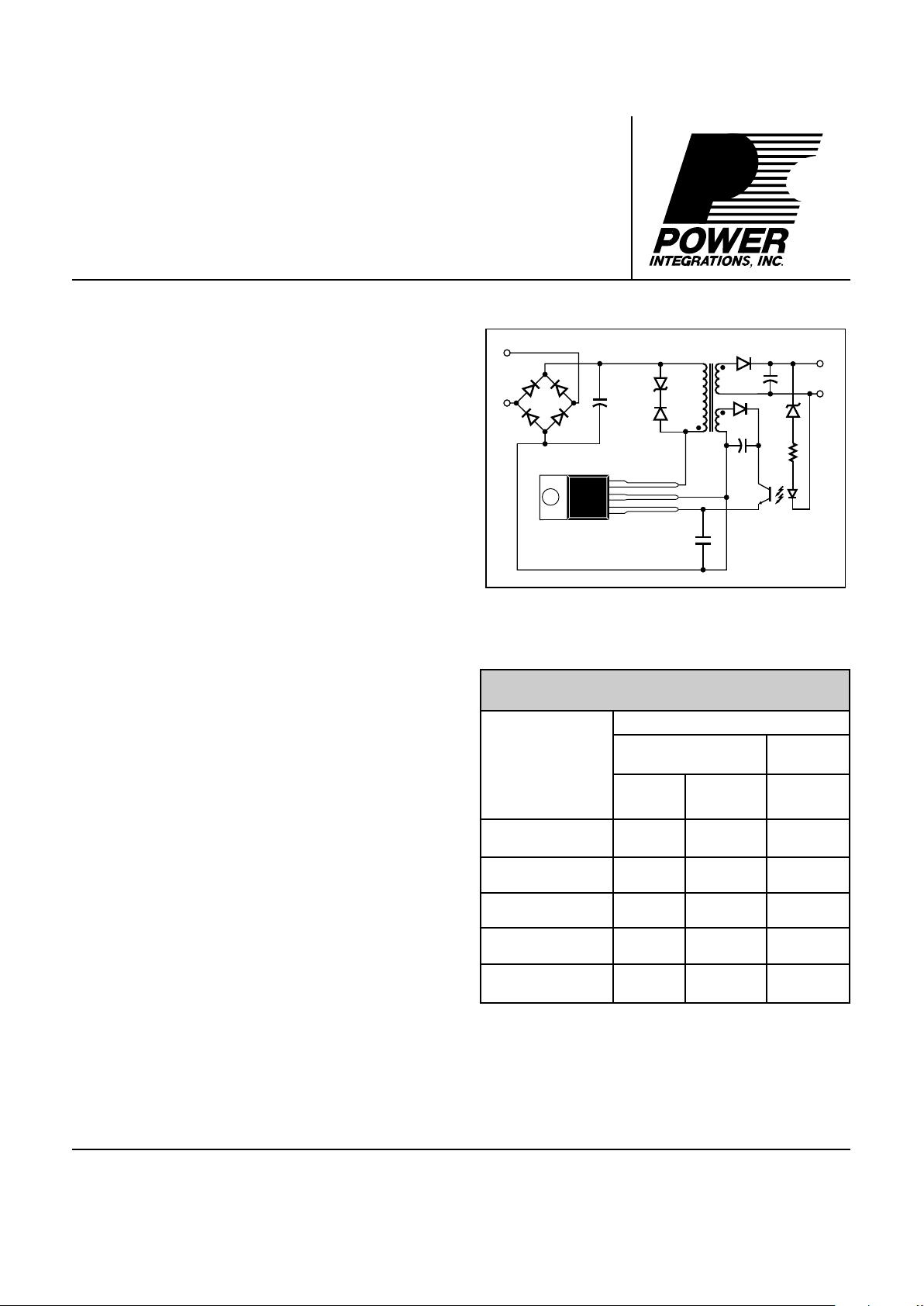
Description
The TOPSwitch family implements, with only three pins, all
functions necessary for an off-line switched mode control
system: high voltage N-channel power MOSFET with controlled
turn-on gate driver, voltage mode PWM controller with
integrated 100 kHz oscillator, high voltage start-up bias circuit,
bandgap derived reference, bias shunt regulator/error amplifier
for loop compensation and fault protection circuitry. Compared
to discrete MOSFET and controller or self oscillating (RCC)
switching converter solutions, a TOPSwitch integrated circuit
can reduce total cost, component count, size, weight and at the
same time increase efficiency and system reliability. These
®
PI-1704112995
AC
IN
DRAIN
SOURCE
CONTROL
TOPSwitch
Figure 1. Typical Application.
TOP100-4
TOPSwitch
Family
Three-terminal Off-line PWM Switch
ORDER
PART
NUMBER
OUTPUT POWER RANGE
TOPSwitch
SELECTION GUIDE
FLYBACK
TOP100YAI* 0-20 W 0-30 W
TOP101YAI* 15-35 W 25-50 W
TOP102YAI* 20-45 W 35-70 W
TOP103YAI* 25-55 W 45-90 W
TOP104YAI* 30-60 W 55-110 W
®
* Package Outline: Y03A
devices are intended for 100/110 VAC off-line Power Supply
applications in the 0 to 60 W range and power factor correction
(PFC) applications in the 0 to 110 W range. They are also well
suited for Telecom, Cablecom and other DC to DC converter
applications in the 0-25 W range (see Design Note DN-16).
100/110 V
VAC
0-6.8 W
6-12 W
8.5-17 W
11-22 W
12-25 W
PFC/
BOOST
100/110
VAC
48 V
DC
Page 2
E
7/96
2
TOP100-4
PI-1746-011796
SHUTDOWN/
AUTO-RESTART
PWM
COMPARATOR
CLOCK
SAW
OSCILLATOR
CONTROLLED
TURN-ON
GATE
DRIVER
INTERNAL
SUPPLY
5.7 V
4.7 V
SOURCE
SRQ
Q
D
MAX
+
CONTROL
+
5.7 V
I
FB
R
E
Z
C
V
C
MINIMUM
ON-TIME
DELAY
+
-
V
I
LIMIT
LEADING
EDGE
BLANKING
POWER-UP
RESET
RSQ
Q
÷ 8
0
1
THERMAL
SHUTDOWN
EXTERNALLY
TRIGGERED
SHUTDOWN
SHUNT REGULATOR/
ERROR AMPLIFIER
+
-
DRAIN
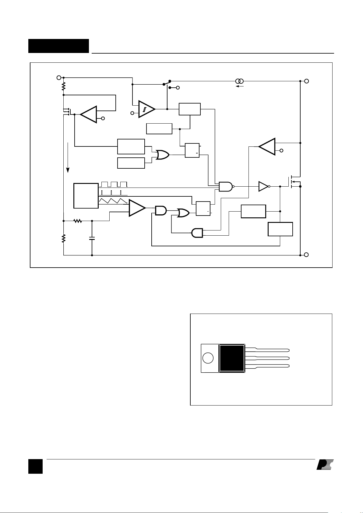
Figure 2. Functional Block Diagram.
Pin Functional Description
DRAIN Pin:
Output MOSFET drain connection. Provides internal bias
current during start-up operation via an internal switched highvoltage current source. Internal current sense point.
CONTROL Pin:
Error amplifier and feedback current input pin for duty cycle
control. Internal shunt regulator connection to provide internal
bias current during normal operation. Trigger input for latching
shutdown. It is also used as the supply bypass and auto-restart/
compensation capacitor connection point.
SOURCE Pin:
Output MOSFET source connection. Primary-side circuit
common, power return, and reference point.
PI-1065A-110194
CONTROL
DRAIN
SOURCE (TAB)
TO-220/3 (YO3A)
Figure 3. Pin Configuration.
Page 3
E
7/96
TOP100-4
3
TOPSwitch
Family Functional Description
TOPSwitch is a self biased and protected
linear control current-to-duty cycle
converter with an open drain output.
High efficiency is achieved through the
use of CMOS and integration of the
maximum number of functions possible.
CMOS significantly reduces bias
currents as compared to bipolar or
discrete solutions. Integration eliminates
external power resistors used for current
sensing and/or supplying initial start-up
bias current.
During normal operation, the internal
output MOSFET duty cycle linearly
decreases with increasing CONTROL
pin current as shown in Figure 4. To
implement all the required control, bias,
and protection functions, the DRAIN
and CONTROL pins each perform
several functions as described below.
Refer to Figure 2 for a block diagram
and Figure 6 for timing and voltage
waveforms of the TOPSwitch integrated
circuit.
Control Voltage Supply
CONTROL pin voltage VC is the supply
or bias voltage for the controller and
driver circuitry. An external bypass
capacitor closely connected between the
CONTROL and SOURCE pins is
required to supply the gate drive current.
The total amount of capacitance
connected to this pin (CT) also sets the
auto-restart timing as well as control
loop compensation. VC is regulated in
either of two modes of operation.
Hysteretic regulation is used for initial
start-up and overload operation. Shunt
regulation is used to separate the duty
cycle error signal from the control circuit
supply current. During start-up, V
C
current is supplied from a high-voltage
switched current source connected
internally between the DRAIN and
CONTROL pins. The current source
provides sufficient current to supply the
control circuitry as well as charge the
total external capacitance (CT).
PI-1691-112895
D
MAX
D
MIN
I
CD1
Duty Cycle (%)
IC (mA)
2.5 6.5 45
Slope = PWM Gain
-16%/mA
I
B
Auto-restart
Figure 4. Relationship of Duty Cycle to CONTROL Pin Current.
Figure 5. Start-up Waveforms for (a) Normal Operation and (b) Auto-restart.
DRAIN
0
V
IN
V
C
0
4.7 V
5.7 V
8 Cycles
95%
5%
Off
Switching Switching
Off
IC
Charging C
T
I
CD1
Discharging C
T
I
CD2
Discharging C
T
IC
Charging C
T
Off
PI-1124A-060694
DRAIN
0
V
IN
V
C
0
4.7 V
5.7 V
Off
Switching
(b)
(a)
CT is the total external capacitance
connected to the CONTROL pin
Page 4

E
7/96
4
TOP100-4
The first time VC reaches the upper
threshold, the high-voltage current
source is turned off and the PWM
modulator and output transistor are
activated, as shown in Figure 5(a).
During normal operation (when the
output voltage is regulated) feedback
control current supplies the VC supply
current. The shunt regulator keeps VC at
typically 5.7 V by shunting CONTROL
pin feedback current exceeding the
required DC supply current through the
PWM error signal sense resistor RE. The
low dynamic impedance of this pin (ZC)
sets the gain of the error amplifier when
used in a primary feedback
configuration. The dynamic impedance
of the CONTROL pin together with the
external resistance and capacitance
determines the control loop
compensation of the power system.
If the CONTROL pin external
capacitance (CT) should discharge to the
lower threshold, then the output
MOSFET is turned off and the control
circuit is placed in a low-current standby
mode. The high-voltage current source
is turned on and charges the external
capacitance again. Charging current is
shown with a negative polarity and
discharging current is shown with a
positive polarity in Figure 6. The
hysteretic auto-restart comparator keeps
VC within a window of typically 4.7 to
5.7 V by turning the high-voltage current
source on and off as shown in Figure
5(b). The auto-restart circuit has a divideby-8 counter which prevents the output
MOSFET from turning on again until
eight discharge-charge cycles have
elapsed. The counter effectively limits
TOPSwitch power dissipation by
reducing the auto-restart duty cycle to
typically 5%. Auto-restart continues to
cycle until output voltage regulation is
again achieved.
Bandgap Reference
All critical TOPSwitch internal voltages
are derived from a temperaturecompensated bandgap reference. This
reference is also used to generate a
temperature-compensated current source
which is trimmed to accurately set the
oscillator frequency and MOSFET gate
drive current.
Oscillator
The internal oscillator linearly charges
and discharges the internal capacitance
between two voltage levels to create a
sawtooth waveform for the pulse width
modulator. The oscillator sets the pulse
width modulator/current limit latch at
the beginning of each cycle. The nominal
frequency of 100 kHz was chosen to
minimize EMI and maximize efficiency
in power supply applications. Trimming
of the current reference improves
oscillator frequency accuracy.
Pulse Width Modulator
The pulse width modulator implements
a voltage-mode control loop by driving
the output MOSFET with a duty cycle
inversely proportional to the current
flowing into the CONTROL pin. The
error signal across RE is filtered by an
RC network with a typical corner
frequency of 7 kHz to reduce the effect
of switching noise. The filtered error
signal is compared with the internal
oscillator sawtooth waveform to generate
the duty cycle waveform. As the control
current increases, the duty cycle
decreases. A clock signal from the
oscillator sets a latch which turns on the
output MOSFET. The pulse width
modulator resets the latch, turning off
the output MOSFET. The maximum
duty cycle is set by the symmetry of the
internal oscillator. The modulator has a
minimum ON-time to keep the current
consumption of the TOPSwitch
independent of the error signal. Note
that a minimum current must be driven
into the CONTROL pin before the duty
cycle begins to change.
Gate Driver
The gate driver is designed to turn the
output MOSFET on at a controlled rate
to minimize common-mode EMI. The
gate drive current is trimmed for
improved accuracy.
Error Amplifier
The shunt regulator can also perform the
function of an error amplifier in primary
feedback applications. The shunt
regulator voltage is accurately derived
from the temperature compensated
bandgap reference. The gain of the error
amplifier is set by the CONTROL pin
dynamic impedance. The CONTROL
pin clamps external circuit signals to the
VC voltage level. The CONTROL pin
current in excess of the supply current is
separated by the shunt regulator and
flows through RE as the error signal.
Cycle-By-Cycle Current Limit
The cycle by cycle peak drain current
limit circuit uses the output MOSFET
ON-resistance as a sense resistor. A
current limit comparator compares the
output MOSFET ON-state drain-source
voltage, V
DS(ON),
with a threshold voltage.
High drain current causes V
DS(ON)
to
exceed the threshold voltage and turns
the output MOSFET off until the start of
the next clock cycle. The current limit
comparator threshold voltage is
temperature compensated to minimize
variation of the effective peak current
limit due to temperature related changes
in output MOSFET R
DS(ON)
.
The leading edge blanking circuit inhibits
the current limit comparator for a short
time after the output MOSFET is turned
on. The leading edge blanking time has
been set so that current spikes caused by
primary-side capacitances and
secondary-side rectifier reverse recovery
time will not cause premature
termination of the switching pulse.
TOPSwitch
Family Functional Description (cont.)
Page 5
E
7/96
TOP100-4
5
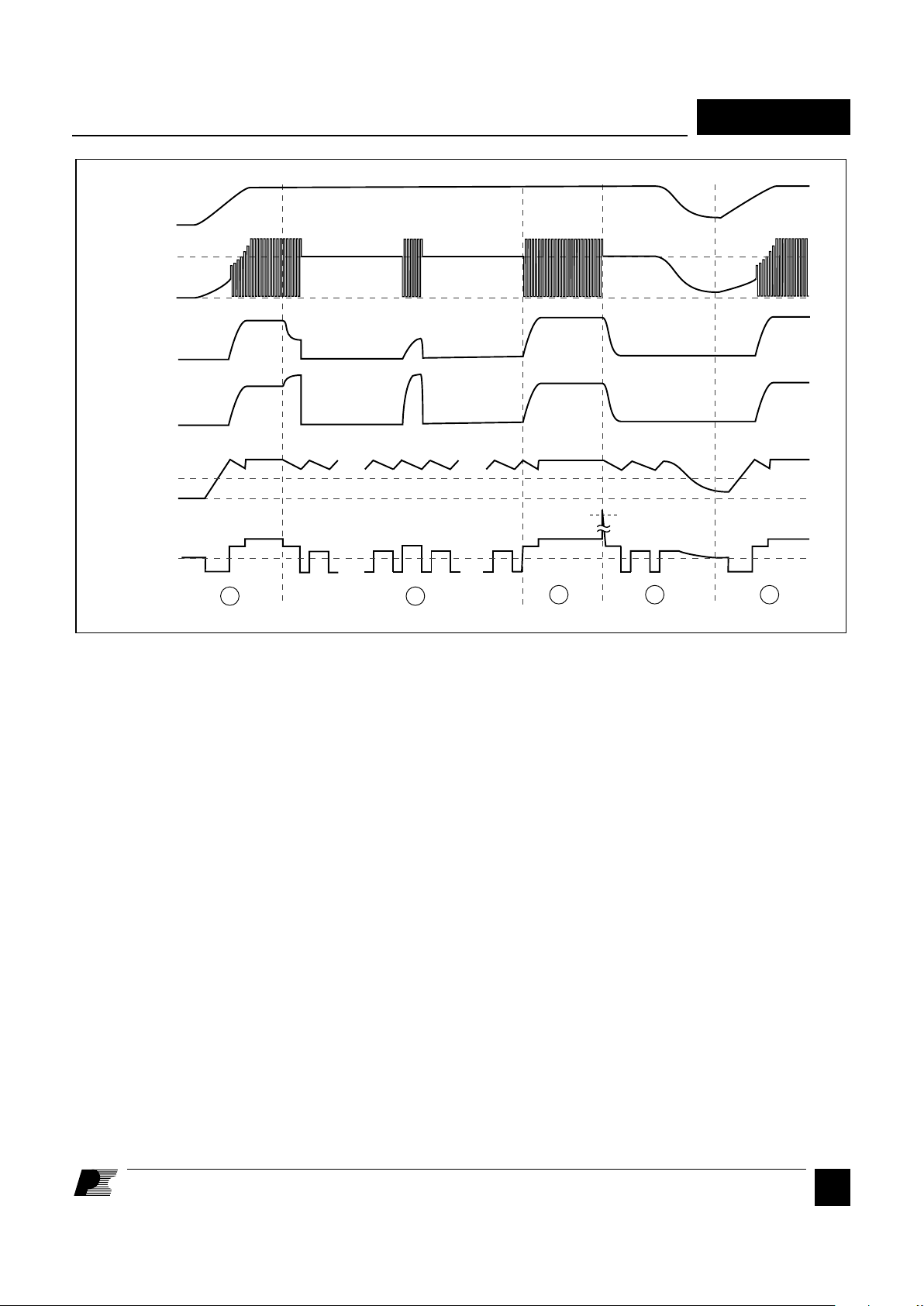
PI-1119-110194
V
IN
V
OUT
0
I
OUT
0
1 2
143
DRAIN
0
V
IN
V
C
0
••• •••
12 12 81
0
I
C
••• •••
12
8
812 81
V
C(reset)
45 mA
Shutdown/Auto-restart
To minimize TOPSwitch power
dissipation, the shutdown/auto-restart
circuit turns the power supply on and off
at a duty cycle of typically 5% if an out
of regulation condition persists. Loss of
regulation interrupts the external current
into the CONTROL pin. VC regulation
changes from shunt mode to the
hysteretic auto-restart mode described
above. When the fault condition is
removed, the power supply output
becomes regulated, VC regulation returns
to shunt mode, and normal operation of
the power supply resumes.
Latching Shutdown
The output overvoltage protection latch
is activated by a high-current pulse into
the CONTROL pin. When set, the latch
turns off the TOPSwitch output.
Activating the power-up reset circuit by
removing and restoring input power, or
momentarily pulling the CONTROL pin
below the power-up reset threshold resets
the latch and allows TOPSwitch to
resume normal power supply operation.
VC is regulated in hysteretic mode when
the power supply is latched off.
Overtemperature Protection
Temperature protection is provided by a
precision analog circuit that turns the
output MOSFET off when the junction
temperature exceeds the thermal
shutdown temperature (typically 145°C).
Activating the power-up reset circuit by
removing and restoring input power or
momentarily pulling the CONTROL pin
below the power-up reset threshold resets
the latch and allows TOPSwitch to
resume normal power supply operation.
VC is regulated in hysteretic mode when
the power supply is latched off.
High-voltage Bias Current Source
This current source biases TOPSwitch
from the DRAIN pin and charges the
CONTROL pin external capacitance
(CT) during start-up or hysteretic
operation. Hysteretic operation occurs
during auto-restart and latched
shutdown. The current source is switched
on and off with an effective duty cycle of
approximately 35%. This duty cycle is
determined by the ratio of CONTROL
pin charge (IC) and discharge currents
(I
CD1
and I
CD2
). This current source is
turned off during normal operation when
the output MOSFET is switching.
Figure 6. Typical Waveforms for (1) Normal Operation, (2) Auto-restart, (3) Latching Shutdown, and (4) Power Down Reset.
Page 6
E
7/96
6
TOP100-4
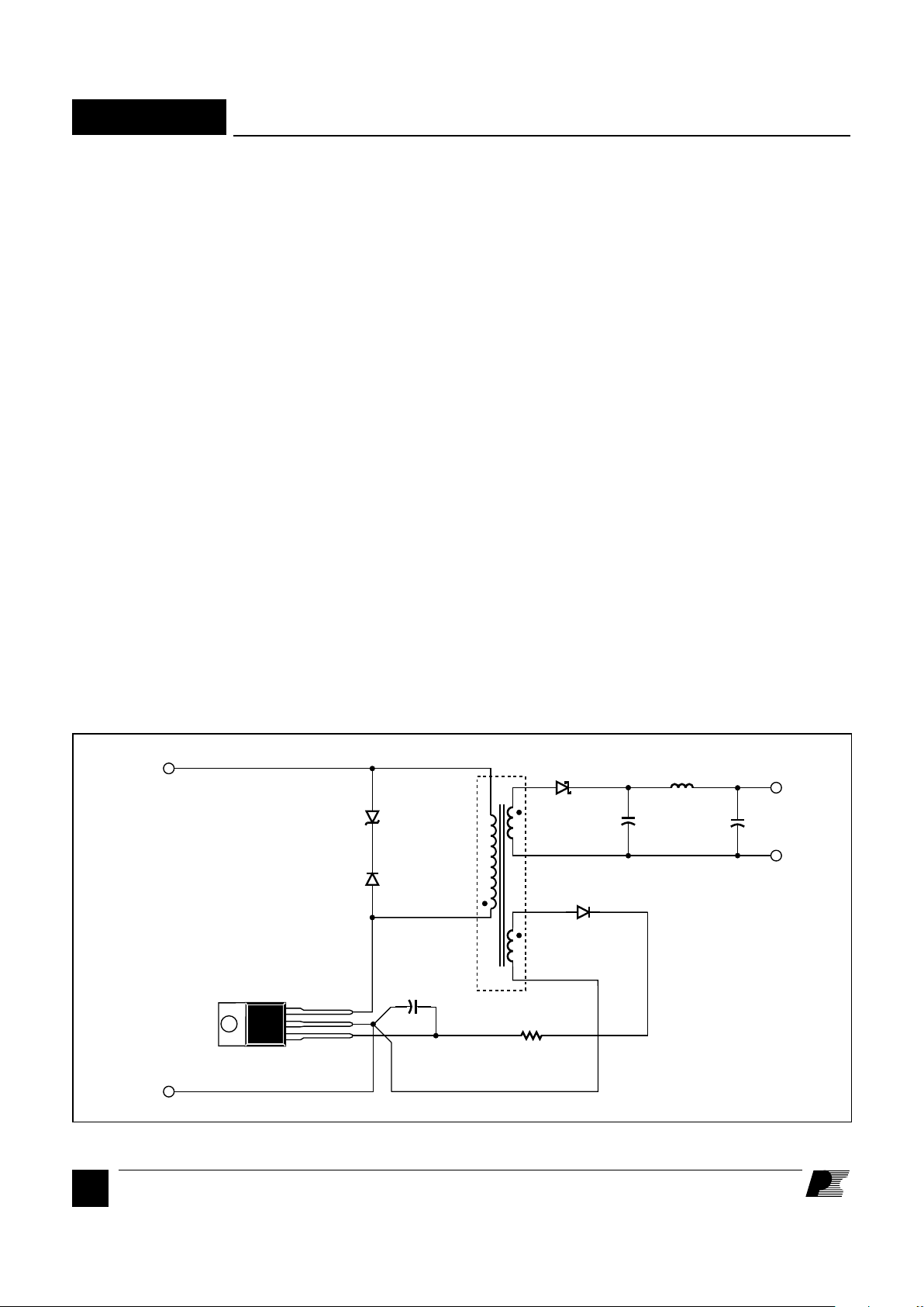
current will flow into the control pin.
Increasing control pin current decreases
the duty cycle until a stable operating
point is reached. The output voltage is
proportional to the bias voltage by the
turns ratio of the output to bias windings.
C5 is used to bypass the CONTROL pin.
C5 also provides loop compensation for
the power supply by shunting AC
currents around the CONTROL pin
dynamic impedance, and also determines
the auto-restart frequency during startup and auto-restart conditions. See DN8 for more information regarding bias
supplies.
General Circuit Operation
Primary Feedback Regulation
The circuit shown in Figure 7 is a simple
5 V, 5 W bias supply using the TOP100.
This flyback power supply employs
primary-side regulation from a
transformer bias winding. This approach
is best for low-cost applications requiring
isolation and operation within a narrow
range of load variation. Line and load
regulation of ±5% or better can be
achieved from 10% to 100% of rated
load.
Voltage feedback is obtained from the
transformer (T1) bias winding, which
eliminates the need for optocoupler and
secondary-referenced error amplifier.
High-voltage DC is applied to the
primary winding of T1. The other side
of the transformer primary is driven by
Figure 7. Schematic Diagram of a Minimum Parts Count 5 V, 5 W Bias Supply Utilizing the TOP100.
the integrated high-voltage MOSFET
transistor within the TOP100 (U1). The
circuit operates at a switching frequency
of 100 kHz, set by the internal oscillator
of the TOP100. The clamp circuit
implemented by VR1 and D1 limits the
leading-edge voltage spike caused by
transformer leakage inductance to a safe
value. The 5 V power secondary winding
is rectified and filtered by D2, C2, C3,
and L1 to create the 5 V output voltage.
The output of the T1 bias winding is
rectified and filtered by D3, R1, and C5.
The voltage across C5 is regulated by
U1, and is determined by the 5.7 V
internal shunt regulator at the
CONTROL pin of U1. When the
rectified bias voltage on C5 begins to
exceed the shunt regulator voltage,
PI-1767-020296
5 V
RTN
C5
47 µF
U1
TOP100YAI
D2
1N5822
D3
1N4148
L1
(Bead)
C2
330 µF
25 V
C3
150 µF
25 V
T1
D1
UF4004
DC
INPUT
VR1
P6KE91
R1
22 Ω
CIRCUIT PERFORMANCE:
Load Regulation - ±4%
(10% to 100%)
Line Regulation - ±1.5%
95 to 185 V DC
Ripple Voltage ±25 mV
DRAIN
SOURCE
CONTROL
Page 7

E
7/96
TOP100-4
7
Simple Optocoupler Feedback
The circuit shown in Figure 8 is a 7.5 V,
15 W secondary regulated flyback power
supply using the TOP101 that will
operate from 85 to 132 VAC input
voltage. Improved output voltage
accuracy and regulation over the circuit
of Figure 7 is achieved by using an
optocoupler and secondary referenced
Zener diode. The general operation of
the power stage of this circuit is the same
as that described for Figure 7.
The input voltage is rectified and filtered
by BR1 and C1. L2, C6 and C7 reduce
conducted emission currents. The bias
winding is rectified and filtered by D3
and C4 to create a typical 11 V bias
voltage. Zener diode (VR2) voltage
together with the forward voltage of the
LED in the optocoupler U2 determine
the output voltage. R1, the optocoupler
current transfer ratio, and the TOPSwitch
control current to duty cycle transfer
function set the DC control loop gain.
C5 together with the control pin dynamic
impedance and capacitor ESR establish
a control loop pole-zero pair. C5 also
determines the auto-restart frequency
and filters internal gate drive switching
currents. R2 and VR2 provide minimum
current loading when output current is
low. See DN-11 for more information
regarding low-cost, 15 W power
supplies.
Accurate Optocoupler Feedback
The circuit shown in Figure 9 is a highly
accurate, 15 V, 30 W secondaryregulated flyback power supply that will
operate from 85 to 132 VAC input
voltage. A TL431 shunt regulator
directly senses and accurately regulates
the output voltage. The effective output
voltage can be fine tuned by adjusting
the resistor divider formed by R4 and
R5. Other output voltages are possible
by adjusting the transformer turns ratios
as well as the divider ratio.
The general operation of the input and
power stages of this circuit are the same
as that described for Figures 7 and 8. R3
and C5 tailor frequency response. The
TL431 (U3) regulates the output voltage
by controlling optocoupler LED current
(and TOPSwitch duty cycle) to maintain
an average voltage of 2.5 V at the TL431
input pin. Divider R4 and R5 determine
the actual output voltage. C9 rolls off
the high frequency gain of the TL431 for
stable operation. R1 limits optocoupler
LED current and determines high
frequency loop gain. For more
information, refer to application note
AN-14.
Figure 8. Schematic Diagram of a 15 W 100/110 VAC Input Power Supply Utilizing the TOP101 and Simple Optocoupler Feedback.
PI-1692-112895
7.5 V
RTN
C5
47µF
10 V
D2
UG8BT
D3
1N4148
R2
68 Ω
VR2
1N5234B
6.2 V
C3
120 µF
25 V
T1
D1
UF4004
C2
680 µF
25 V
VR1
P6KE91
CIRCUIT PERFORMANCE:
Line Regulation - ±0.5%
(85-132 VAC)
Load Regulation - ±1%
(10-100%)
Ripple Voltage ±50 mV
Meets CISPR-22 Class B
BR1
200 V
C1
27 µF
200 V
R1
39 Ω
U2
NEC2501
U1
TOP101YAI
DRAIN
SOURCE
CONTROL
C4
0.1 µF
C7
1 nF
Y1
L1
3.3 µH
F1
3.15 A
J1
C6
0.1 µF
L2
20 mH
L
N
Page 8

E
7/96
8
TOP100-4
Figure 10. Schematic Diagram of a 60 W 110 VAC Input Boost Power Factor Correction Circuit Utilizing the TOP103.
Figure 9. Schematic Diagram of a 30 W 100/110 VAC Input Power Supply Utilizing the TOP102 and Accurate Optocoupler Feedback.
PI-1693-112895
15 V
RTN
BR1
200 V
C1
47 µF
200 V
C5
47 µF
C4
0.1 µF
U1
TOP102YAI
R3
6.2 Ω
R2
200 Ω
1/2 W
D2
MUR610CT
D3
1N4148
C2
1000 µF
35 V
T1
D1
BYV26B
C7
1 nF
Y1
DRAIN
SOURCE
CONTROL
C3
120 µF
25 V
U2
NEC2501
U3
TL431
R4
49.9 kΩ
R5
10 kΩ
C9
0.1 µF
R1
510 Ω
VR1
P6KE91
L1
3.3 µH
F1
3.15 A
J1
C6
0.1 µF
L2
33 mH
L
N
CIRCUIT PERFORMANCE:
Line Regulation - ±0.2%
(85-132 VAC)
Load Regulation - ±0.2%
(10-100%)
Ripple Voltage ±150 mV
Meets CISPR-22 Class B
PI-1437-042595
PFC OUT
RTN
D1
MUR440
BR1
200 V
R1
130 kΩ
R2
200 Ω
R10
6.8 kΩ
R3
3 kΩ
VR1
120 V
VR2
120 V
D2
1N4936
C1
220 nF
200 V
C4
100 µF
C2
4.7 µF
C3
220 µF
L1
380 µH
EMI
FILTER
AC
IN
U1
TOP103YAI
DRAIN
SOURCE
CONTROL
TYPICAL PERFORMANCE:
Power Factor = 0.99
THD =5%
Page 9

E
7/96
TOP100-4
9
by the boost inductance and parasitic
capacitance. R1 generates a precompensation current proportional to
the instantaneous rectified AC input
voltage which directly varies the duty
cycle. C2 filters high frequency
switching currents while having no
filtering effect on the line frequency precompensation current. R2 decouples
the pre-compensation current from the
large filter capacitor C3 to prevent an
averaging effect which would increase
total harmonic distortion. C1 filters
high frequency noise currents which
could cause errors in the precompensation current.
General Circuit Operation (cont.)
When power is first applied, C3 charges
to typically 5.7 volts before TOPSwitch
starts. C3 then provides TOPSwitch
bias current until the output voltage
becomes regulated. When the output
voltage becomes regulated, series
connected Zener diodes VR1 and VR2
begin to conduct, drive current into the
TOPSwitch control pin, and directly
control the duty cycle. C3 together with
R3 perform low pass filtering on the
feedback signal to prevent output line
frequency ripple voltage from varying
the duty cycle. For more information,
refer to Design Note DN-7.
Keep the SOURCE pin length very short.
Use a Kelvin connection to the SOURCE
pin for the CONTROL pin bypass
capacitor. Use single point grounding
techniques at the SOURCE pin as shown
in Figure 11.
Minimize peak voltage and ringing on
the DRAIN voltage at turn-off. Use a
Zener or TVS Zener diode to clamp the
DRAIN voltage.
Do not plug the TOPSwitch device into
a “hot” IC socket during test. External
CONTROL pin capacitance may deliver
a surge current sufficient to trigger the
shutdown latch which turns the
TOPSwitch off.
Under some conditions, externally
provided bias or supply current driven
into the CONTROL pin can hold the
TOPSwitch in one of the 8 auto-restart
cycles indefinitely and prevent starting.
Shorting the CONTROL pin to the
SOURCE pin will reset the TOPSwitch.
To avoid this problem when doing bench
evaluations, it is recommended that the
VC power supply be turned on before the
DRAIN voltage is applied.
CONTROL pin currents during autorestart operation are much lower at low
input voltages (< 20 V) which increases
the auto-restart cycle period (see the I
C
vs. Drain Voltage Characteristic curve).
Short interruptions of AC power may
cause TOPSwitch to enter the 8-count
auto-restart cycle before starting again.
This is because the input energy storage
capacitors are not completely discharged
and the CONTROL pin capacitance has
not discharged below the pin internal
power-up reset voltage.
In some cases, minimum loading may
be necessary to keep a lightly loaded or
unloaded output voltage within the
desired range due to the minimum ONtime.
For additional applications information
regarding the TOPSwitch family, refer
to AN-14.
Key Application Issues
Figure 11. Recommended TOPSwitch Layout.
PI-1240-110194
PC Board
Kelvin-connected
bypass capacitor
and/or compensation network
Bias/Feedback Input
Bias/Feedback Return
High-voltage Return
Bend DRAIN pin
forward if needed
for creepage
DRAIN
SOURCE
CONTROL
Do not bend SOURCE pin
Keep it short
High Voltage
Return
Bias/Feedback
Return
Bypass
Capacitor
D
S
C
TOP VIEW
Bias/Feedback
Input
Boost PFC Pre-regulator
TOPSwitch can also be used as a fixed
frequency, discontinuous mode boost
pre-regulator to improve Power Factor
and reduce Total Harmonic Distortion
(THD) for applications such as power
supplies and electronic ballasts. The
circuit shown in Figure 10 operates from
110 VAC and delivers 60 W at 265 VDC
with typical Power Factor over 0.99 and
THD of 5%. Bridge Rectifier BR1 full
wave rectifies the AC input voltage. L1,
D1, C4, and TOPSwitch make up the
boost power stage. D2 prevents reverse
current through the TOPSwitch body
diode due to ringing voltages generated
Page 10

E
7/96
10
TOP100-4
IC = 4 mA, Tj = 25˚C
IC = I
CD1
+ 0.5 mA, See Figure 12
IC = 10 mA, See Figure 12
IC = 4 mA, Tj = 25˚C
See Figure 4
See Note 1
See Figure 4
IC = 4 mA, Tj = 25˚C
See Figure 13
Tj = 25˚C
See Note 1
S1 open
Conditions
(Unless Otherwise Specified)
Specification Symbol See Figure 14 Min Typ Max Units
SOURCE = 0 V
Tj = -40 to 125°C
ABSOLUTE MAXIMUM RATINGS
(1)
DRAIN Voltage ............................................ -0.3 to 350 V
CONTROL Voltage ..................................... - 0.3 V to 9 V
Storage Temperature ......................................-65 to 125°C
Operating Junction Temperature
(2)
.................-40 to 150°C
Lead Temperature
(3)
................................................. 260°C
Thermal Impedance (θJA) ...................................... 70°C/W
Thermal Impedance (θJC)
(4)
.................................... 2 °C/W
1. Unless noted, all voltages referenced to SOURCE,
TA = 25°C.
2. Normally limited by internal circuitry.
3. 1/16" from case for 5 seconds.
4. Measured at tab closest to plastic interface.
90 100 110
64 67 70
1.0 1.8 3.0
-11 -16 -21
-0.05
1.5 2.5 4
10 15 22
0.18
-2.4 -1.9 -1.2
-2 -1.5 -0.8
0.4
5.7
f
OSC
DC
MAX
DC
MIN
I
B
Z
C
I
C
CONTROL FUNCTIONS
Output
Frequency
Maximum
Duty Cycle
Minimum
Duty Cycle
PWM
Gain
PWM Gain
Temperature Drift
External
Bias Current
Dynamic
Impedance
Dynamic Impedance
Temperature Drift
CONTROL Pin
Charging Current
Charging Current
Temperature Drift
Auto-restart
Threshold Voltage
kHz
%
%
%/mA
%/mA/˚C
mA
Ω
%/˚C
mA
%/˚C
V
SHUTDOWN/AUTO-RESTART
VC = 0 V
VC = 5 V
V
C(AR)
Page 11

E
7/96
TOP100-4
11
4.7
0.6 1.0
58
1.2
0.88 1.25
1.50 2.15
2.20 3.10
2.85 4.00
3.30 4.60
150
100
125 145
25 45 75
2.0 3.3 4.2
S1 open
S1 open
S1 open
S1 open
TOP100
di/dt = 160 mA/µs, Tj = 25˚C
TOP101
di/dt = 280 mA/µs, Tj = 25˚C
TOP102
di/dt = 400 mA/µs, Tj = 25˚C
TOP103
di/dt = 520 mA/µs, Tj = 25˚C
TOP104
di/dt = 600 mA/µs, Tj = 25˚C
IC = 4 mA
IC = 4 mA
IC = 4 mA
See Figure 13
S2 open
I
LIMIT
t
LEB
t
ILD
I
SD
V
C(RESET)
V
V
%
Hz
A
ns
ns
°C
mA
V
SHUTDOWN/AUTO-RESTART (cont.)
UV Lockout
Threshold Voltage
Auto-restart
Hysteresis Voltage
Auto-restart
Duty Cycle
Auto-restart
Frequency
Self-protection
Current Limit
Leading Edge
Blanking Time
Current Limit
Delay
Thermal Shutdown
Temperature
Latched Shutdown
Trigger Current
Power-up Reset
Threshold Voltage
CIRCUIT PROTECTION
Conditions
(Unless Otherwise Specified)
Specification Symbol See Figure 14 Min Typ Max Units
SOURCE = 0 V
Tj = -40 to 125°C
Page 12

E
7/96
12
TOP100-4
R
DS(ON)
I
DSS
BV
DSS
t
r
t
f
V
C(SHUNT)
I
CD1
I
CD2
TOP100 Tj = 25°C
ID = 110 mA Tj = 100°C
TOP101 Tj = 25°C
ID = 190 mA Tj = 100°C
TOP102 Tj = 25°C
ID = 270 mA Tj = 100°C
TOP103 Tj = 25°C
ID = 350 mA Tj = 100°C
TOP104 Tj = 25°C
ID = 400 mA Tj = 100°C
Device in Latched Shutdown
IC = 4 mA, VDS = 280 V, TA = 125°C
Device in Latched Shutdown
IC = 4 mA, ID = 500 µA, TA = 25°C
Measured With
Figure 8 Schematic
Measured With
Figure 8 Schematic
See Note 2
IC = 4 mA
Output MOSFET Enabled
Output MOSFET Disabled
ON-State
Resistance
OFF-State
Current
Breakdown
Voltage
Rise
Time
Fall
Time
DRAIN Supply
Voltage
Shunt Regulator
Voltage
Shunt Regulator
Temperature Drift
CONTROL Supply/
Discharge Current
Ω
µA
V
ns
ns
V
V
ppm/˚C
mA
OUTPUT
SUPPLY
Conditions
(Unless Otherwise Specified)
Specification Symbol See Figure 14 Min Typ Max Units
SOURCE = 0 V
Tj = -40 to 125°C
6.4 7.5
10.5 12.4
3.6 4.3
6.0 7.1
2.6 3.0
4.2 5.0
2.0 2.4
3.3 3.9
1.7 2.0
2.8 3.3
500
350
100
50
36
5.5 5.8 6.1
±50
0.6 1.2 1.6
0.5 0.8 1.1
Page 13

E
7/96
TOP100-4
13
Conditions
(Unless Otherwise Specified)
Specification Symbol See Figure 14 Min Typ Max Units
VS2 = 16 V R1 = 0 Ω
SOURCE = 0 V
Tj = -40 to 125°C
LOW INPUT VOLTAGE OPERATION (See Note 3)
16
-2.3 -1.65 -1
-1.2 -0.64 -0.28
48
0.85
Volts
mA
mA
%
Hz
DRAIN Supply
Voltage
CONTROL Pin
Charging Current
Auto-restart
Duty Cycle
Auto-restart
Frequency
NOTES:
1. For specifications with negative values, a negative temperature coefficient corresponds to an increase in
magnitude with increasing temperature, and a positive temperature coefficient corresponds to a decrease in
magnitude with increasing temperature.
2. It is possible to start up and operate
TOPSwitch
at DRAIN voltages well below 36 V. Refer to the "Low Input
Voltage" Specification section for details.
3. This section specifies only parameters affected by low input voltage operation (Drain Voltages less than 36 V). All
other parameters remain unchanged.
4. For low input voltage applications, the primary peak current could be set to a lower value than the current limit to
increase efficiency. Refer to the Output Characteristics graph (Drain Current vs. Drain Voltage). The voltage
across the transformer primary during the ON time is the difference between the input voltage and the drain
voltage (V
DS(ON)
).
For example, if the input voltage is 16 VDC and a TOP104 (3.3A minimum current limit) is used at a primary peak
current of 1A. Then the (V
DS(ON)
) is 3 V at 100°C and the energizing voltage across the transformer primary is
13 V.
VC= 0 V
VC= 5 V
See Note 4
Tj = 25°C
S1/Open
S1/Open
Page 14

E
7/96
14
TOP100-4
PI-1215-091794
DRAIN
VOLTAGE
HV
0 V
90%
10%
90%
t
2
t
1
DC =
t1
t
2
Figure 12. TOPSwitch Duty Cycle Measurement.
PI-1905-061396
C1
0.1 µF
C2
47 µF
VS1
0-50 V
VS2
40 V
TOPSwitch
R1
470 Ω
5 W
S2
S1
R2
470 Ω
DRAIN
SOURCE
CONTROL
NOTE: This test circuit is not applicable for current limit or output characteristic measurements.
Figure 14. TOPSwitch General Test Circuit.
120
100
80
40
20
60
0
0246810
CONTROL Pin Voltage (V)
CONTROL Pin Current (mA)
TYPICAL CONTROL PIN I-V CHARACTERISTIC
PI-1216-091794
Latched Shutdown
Trigger Current (45 mA)
1
Slope
Dynamic
Impedance
=
Figure 13. TOPSwitch CONTROL Pin I-V Characteristic.
Page 15

E
7/96
TOP100-4
15
1.1
1.0
0.9
-50 -25 0 25 50 75 100 125 150
Junction Temperature (°C)
Breakdown Voltage (V)
(Normalized to 25°C)
BREAKDOWN vs. TEMPERATURE
PI-176B-051391
1.2
1.0
0.8
0.6
0.4
0.2
0
-50 -25 0 25 50 75 100 125 150
Junction Temperature (°C)
FREQUENCY vs. TEMPERATURE
PI-1123A-060794
Output Frequency
(Normalized to 25°C)
1.2
1.0
0.8
0.6
0.4
0.2
0
-50 -25 0 25 50 75 100 125 150
Junction Temperature (°C)
CURRENT LIMIT vs. TEMPERATURE
PI-1125-041494
Current Limit
(Normalized to 25°C)
2
1.2
1.6
0
0 20406080100
Drain Voltage (V)
CONTROL Pin
Charging Current (mA)
IC vs. DRAIN VOLTAGE
PI-1145-103194
0.4
0.8
VC = 5 V
The control pin voltage will be oscillating
at a low frequency from 4.7 to 5.7 V and
the DRAIN is turned on every eighth
cycle of the CONTROL pin oscillation.
If the CONTROL pin power supply is
turned on while in this auto-restart mode,
there is only a 12.5% chance that the
control pin oscillation will be in the
correct state (DRAIN active state) so
The following precautions should be
followed when testing TOPSwitch by
itself outside of a power supply. The
schematic shown in Figure 14 is
suggested for laboratory testing of
TOPSwitch.
When the DRAIN supply is turned on,
the part will be in the auto-restart mode.
BENCH TEST PRECAUTIONS FOR EVALUATION OF ELECTRICAL CHARACTERISTICS
that the continuous DRAIN voltage
waveform may be observed. It is
recommended that the VC power supply
be turned on first and the DRAIN power
supply second if continuous drain voltage
waveforms are to be observed. The
12.5% chance of being in the correct
state is due to the 8:1 counter.
Typical Performance Characteristics
Page 16

E
7/96
16
TOP100-4
Typical Performance Characteristics (cont.)
5
3
4
0
0468210
Drain Current (A)
OUTPUT CHARACTERISTICS
PI-1747-011796
1
2
Drain Voltage (V)
T
CASE
= 25°C
T
CASE
= 100°C
Scaling Factors:
TOP104 1.00
TOP103 0.87
TOP102 0.67
TOP101 0.47
TOP100 0.27
1000
10
0 24016080 320
DRAIN Voltage (V)
DRAIN Capacitance (pF)
C
OSS
vs. DRAIN VOLTAGE
100
PI-1439-042595
Scaling Factors:
TOP104 1.00
TOP103 0.87
TOP102 0.67
TOP101 0.47
TOP100 0.27
100
50
0
0 16080 240 320
DRAIN Voltage (V)
Power (mW)
DRAIN CAPACITANCE POWER
PI-1694-112895
Scaling Factors:
TOP104 1.00
TOP103 0.87
TOP102 0.67
TOP101 0.47
TOP100 0.27
Page 17

E
7/96
TOP100-4
17
B
K
F
G
C
J
L
M
E
A
D
DIM
A
B
C
D
E
F
G
H
J
K
L
M
N
O
P
PI-1848-050696
inches
.460-.480
.400-.415
.236-.260
.240 - REF.
.520-.560
.028-.038
.045-.055
.090-.110
.165-.185
.045-.055
.095-.115
.015-.020
.705-.715
.146-.156
.103-.113
mm
11.68-12.19
10.16-10.54
5.99-6.60
6.10 - REF.
13.21-14.22
.71-.97
1.14-1.40
2.29-2.79
4.19-4.70
1.14-1.40
2.41-2.92
.38-.51
17.91-18.16
3.71-3.96
2.62-2.87
H
* LEADS AND TAB ARE
SOLDER PLATED
N
O
P
Notes:
1. Package dimensions conform to
JEDEC specification TO-220 AB for
standard flange mounted, peripheral
lead package; .100 inch lead spacing
(Plastic) 3 leads (issue J, March 1987)
2. Controlling dimensions are inches.
3. Pin numbers start with Pin 1, and
continue from left to right when
viewed from the top.
4. Dimensions shown do not include
mold flash or other protrusions. Mold
flash or protrusions shall not exceed
.006 (.15 mm) on any side.
5. Position of terminals to be
measured at a position .25 (6.35 mm)
from the body.
6. All terminals are solder plated.
Y03A Plastic TO-220/3
Page 18

E
7/96
18
TOP100-4
NOTES
Page 19

E
7/96
TOP100-4
19
NOTES
Page 20

E
7/96
20
TOP100-4
JAPAN
Power Integrations, K.K.
Keihin-Tatemono 1st Bldg.
12-20 Shin-Yokohoma 2-Chome, Kohoku-ku
Yokohama-shi, Kanagawa 222 Japan
Phone: 81•(0)•45•471•1021
Fax: 81•(0)•45•471•3717
ASIA & OCEANIA
For Your Nearest Sales/Rep Office
Please Contact Customer Service
Phone: 408•523•9265
Fax: 408•523•9365
WORLD HEADQUARTERS
Power Integrations, Inc.
477 N. Mathilda Avenue
Sunnyvale, CA 94086
USA
Main: 408•523•9200
Customer Service:
Phone: 408•523•9265
Fax: 408•523•9365
AMERICAS
For Your Nearest Sales/Rep Office
Please Contact Customer Service
Phone: 408•523•9265
Fax: 408•523•9365
Power Integrations reserves the right to make changes to its products at any time to improve reliability or manufacturability.
Power Integrations does not assume any liability arising from the use of any device or circuit described herein, nor does it
convey any license under its patent rights or the rights of others.
PI Logo and
TOPSwitch
are registered trademarks of Power Integrations, Inc.
©Copyright 1994, Power Integrations, Inc. 477 N. Mathilda Avenue, Sunnyvale, CA 94086
APPLICATIONS HOTLINE
World Wide 408•523•9260
APPLICATIONS FAX
Americas 408•523•9361
Europe/Africa
44•(0)•1753•622•209
Japan 81•(0)•45•471•3717
Asia/Oceania 408•523•9364
EUROPE & AFRICA
Power Integrations (Europe) Ltd.
Mountbatten House
Fairacres
Windsor SL4 4LE
United Kingdom
Phone: 44•(0)•1753•622•208
Fax: 44•(0)•1753•622•209
 Loading...