

Page 1

TMS320VC33
DIGITAL SIGNAL PROCESSOR
SPRS087A – FEBRUARY 1999 – REVISED DECEMBER 1999
1
POST OFFICE BOX 1443 • HOUSTON, TEXAS 77251–1443
D High-Performance Floating-Point Digital
Signal Processor (DSP):
– TMS320VC33-150
13-ns Instruction Cycle Time
150 MFLOPS, 75 MIPS
– TMS320VC33-120
17-ns Instruction Cycle Time
120 MFLOPS, 60 MIPS
D 34K × 32-Bit (1.1-Mbit) On-Chip Words of
Dual Access SRAM Configured in 2 × 16K
plus 2 × 1K Blocks to improve Internal
Performance
D x5 PLL Clock Generator
D Very Low Power: < 200 mW @ 150 MFLOPS
D 32-Bit High-Performance CPU
D 16-/32-Bit Integer and 32-/40-Bit
Floating-Point Operations
D Four Internally Decoded Page Strobes to
Simplify Interface to I/O and Memory
Devices
D 32-Bit Instruction Word, 24-Bit Addresses
D EDGEMODE Selectable External Interrupts
D Boot-Program Loader
D On-Chip Memory-Mapped Peripherals:
– One Serial Port
– Two 32-Bit Timers
– Direct Memory Access (DMA)
Coprocessor for Concurrent I/O and CPU
Operation
D Fabricated Using the 0.18-Micron
(l
eff
-effective gate length) TImeline
Technology by Texas Instruments (TI)
D 144-Pin Thin Quad Flat Pack (TQFP)
(PGE Suffix)
D Eight Extended-Precision Registers
D T wo Address Generators With Eight
Auxiliary Registers and Two Auxiliary
Register Arithmetic Units (ARAUs)
D Two Low-Power Modes
D Two- and Three-Operand Instructions
D Parallel Arithmetic/Logic Unit (ALU) and
Multiplier Execution in a Single Cycle
D Block-Repeat Capability
D Zero-Overhead Loops With Single-Cycle
Branches
D Conditional Calls and Returns
D Interlocked Instructions for
Multiprocessing Support
D Bus-Control Registers Configure
Strobe-Control Wait-State Generation
D 1.8-V (Core) and 3.3-V (I/O) Supply Voltages
D On-Chip Scan-Based Emulation Logic,
IEEE Std 1149.1† (JTAG)
description
The TMS320VC33 DSP is a 32-bit, floating-point processor manufactured in 0.18-micron four-level-metal
CMOS (TImeline) technology. The TMS320VC33 is part of the TMS320C3x generation of DSPs from Texas
Instruments.
The TMS320C3x’s internal busing and special digital-signal-processing instruction set have the speed and
flexibility to execute up to 150 million floating-point operations per second (MFLOPS). The TMS320C3x
optimizes speed by implementing functions in hardware that other processors implement through software or
microcode. This hardware-intensive approach provides performance previously unavailable on a single chip.
The TMS320C3x can perform parallel multiply and ALU operations on integer or floating-point data in a single
cycle. Each processor also possesses a general-purpose register file, a program cache, dedicated ARAUs,
internal dual-access memories, one DMA channel supporting concurrent I/O, and a short machine-cycle time.
High performance and ease of use are results of these features.
Please be aware that an important notice concerning availability, standard warranty, and use in critical applications of
Texas Instruments semiconductor products and disclaimers thereto appears at the end of this data sheet.
PR
O
DU
C
T PREVIEW
PRODUCT PREVIEW information concerns products in the formative or
design phase of development. Characteristic data and other
specifications are design goals. Texas Instruments reserves the right to
change or discontinue these products without notice.
TImeline and TI are trademarks of Texas Instruments Incorporated.
Copyright 1999, Texas Instruments Incorporated
†
IEEE Standard 1149.1-1990 Standard-Test-Access Port and Boundary Scan Architecture.
Page 2
TMS320VC33
DIGITAL SIGNAL PROCESSOR
SPRS087A – FEBRUARY 1999 – REVISED DECEMBER 1999
2
POST OFFICE BOX 1443 • HOUSTON, TEXAS 77251–1443
description (continued)
General-purpose applications are greatly enhanced by the large address space, multiprocessor interface,
internally and externally generated wait states, one external interface port, two timers, one serial port, and
multiple-interrupt structure. The TMS320C3x supports a wide variety of system applications from host
processor to dedicated coprocessor. High-level-language support is easily implemented through a
register-based architecture, large address space, powerful addressing modes, flexible instruction set, and
well-supported floating-point arithmetic.
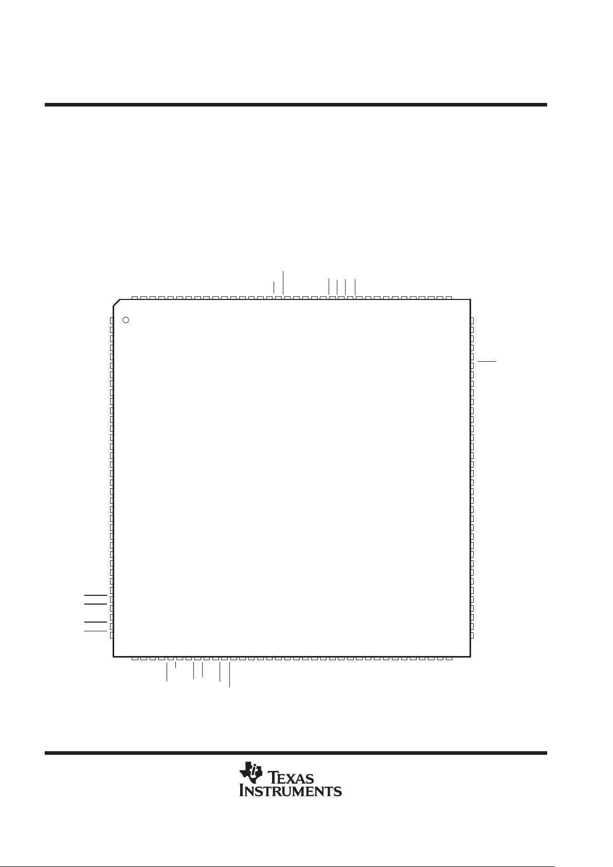
TMS320VC33 pinout (top view)
MCBL/MP
RESET
DV
DD
CLKR0
FSR0
V
SS
DR0
TRST
TMS
CV
DD
TDI
TDO
TCK
V
SS
EMU0
EMU1
DV
DD
D0
D1
D2
D3
V
SS
D4
D5
DV
DD
D6
D7
CV
DD
D8
D9
V
SS
D10
D11
DV
DD
D12
D13
D14
D15
A20
V
SS
A19
A18
A17
DV
DD
A16
A15
V
SS
A14
A13
CV
DD
A12
A11
DV
DD
A10
A9
V
SS
A8
A7
A6
A5
DV
DD
A4
V
SS
A3
A2
CV
DD
A1
A0
DV
DD
PAGE3
PAGE2
V
SS
PAGE1
PAGE0
144
A22
143
142
141
140
RSV0
139
RSV1
138
137
CLKMD0
136
CLKMD1
135
134
XIN
133
XOUT
132
131
EXTCLK
130
129
128
127
126
125
EDGEMODE
124
123
INT0
122
INT1
121
INT2
120
INT3
119
118
117
XF1
116
115
TCLK0
114
TCLK1
113
112
373839404142434445464748495051525354555657585960616263646566676869
1
2
3
4
5
6
7
8
9
10
11
12
13
14
15
16
17
18
19
20
21
22
23
24
25
26
27
28
29
30
31
32
33
34
35
36
108
107
106
105
104
103
102
101
100
99
98
97
96
95
94
93
92
91
90
89
88
87
86
85
84
83
82
81
80
79
78
77
76
75
74
73
H1
H3
STRB
R/W
IACK
RDY
HOLD
HOLDA
D25
D24
D23
D22
D21
D20
D19
D17
D27
D30
111
DX0
110
CLKX0
109
707172
D16
XF0
FSX0
DD
DV
SHZ
TMS320VC33 PGE PACKAGE
†‡
(TOP VIEW)
A23
D28
A21
DD
DV
DD
DV
DD
PLLV
DD
DV
DD
DV
DD
DV
DD
DV
DD
CV
DD
CV
DD
CV
DD
CV
D31
SS
V
SS
V
SS
PLLV
SS
V
SS
V
SS
V
SS
V
D29
D26
D18
DD
DV
SS
V
SS
V
SS
V
†
DVDD is the power supply for the I/O pins while CVDD is the power supply for the core CPU. VSS is the ground for both the I/O
pins and the core CPU.
‡
PLLVDD and PLLVSS are isolated PLL supply pins that should be externally connected to CVDD and V
SS,
respectively.
The TMS320VC33 device is packaged in 144-pin thin quad flatpacks (PGE Suffix).
PR
O
DU
C
T PREVIEW
Page 3
TMS320VC33
DIGITAL SIGNAL PROCESSOR
SPRS087A – FEBRUARY 1999 – REVISED DECEMBER 1999
3
POST OFFICE BOX 1443 • HOUSTON, TEXAS 77251–1443
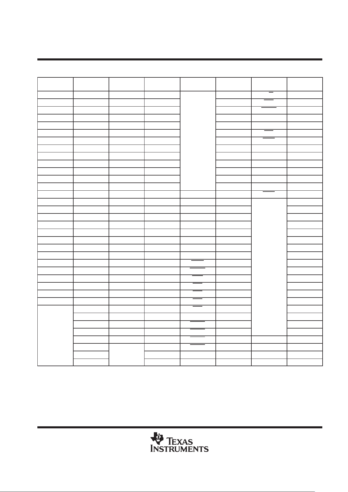
TMS320VC33 Terminal Assignments (Alphabetical)
SIGNAL
NAME
PIN
NUMBER
SIGNAL
NAME
PIN
NUMBER
SIGNAL
NAME
PIN
NUMBER
SIGNAL
NAME
PIN
NUMBER#
A0 30 D0 93 31 R/W 42
A1 29 D1 92 37 RDY 45
A2 27 D2 91 43 RESET 127
A3 26 D3 90 53 RSV0 139
A4 24 D4 88 60 RSV1 138
A5 22 D5 87 69 SHZ 128
A6 21 D6 85
DV
DD
†
77 STRB 41
A7 20 D7 84
DV
DD
†
86 TCK 98
A8 19 D8 82 94 TCLK0 114
A9 17 D9 81 108 TCLK1 113
A10 16 D10 79 115 TDI 100
A11 14 D11 78 129 TDO 99
A12 13 D12 76 143 TMS 102
A13 11 D13 75 DX0 111 TRST 103
A14 10 D14 74 EDGEMODE 124 2
A15 8 D15 73 EMU0 96 9
A16 7 D16 71 EMU1 95 18
A17 5 D17 70 EXTCLK 130 25
A18 4 D18 68 FSR0 106 34
A19 3 D19 67 FSX0 110 40
A20 1 D20 65 H1 38 49
A21 144 D21 64 H3 39 56
A22 142 D22 62 HOLD 47
63
A23 141 D23 61 HOLDA 48
V
SS
72
CLKMD0 136 D24 59 IACK 44 80
CLKMD1 135 D25 58 INT0 122 89
CLKR0 107 D26 57 INT1 121 97
CLKX0 109 D27 55 INT2 120 105
12 D28 54 INT3 119 112
28 D29 52 MCBL/MP 125 118
46 D30 51 PAGE0 36 126
66 D31 50 PAGE1 35 140
CV
DD
83 DR0 104 PAGE2 33 XIN 133
101 6 PAGE3 32 XOUT 132
123
DV
DD
15 PLLV
DD
‡
131 XF0 117
137
DV
DD
23 PLLV
SS
‡
134 XF1 116
†
DVDD is the power supply for the I/O pins while CVDD is the power supply for the core CPU. VSS is the ground for both the I/O pins and the core
CPU.
‡
PLLVDD and PLLVSS are isolated PLL supply pins that should be externally connected to CVDD and VSS respectively.
PR
O
DU
C
T PREVIEW
Page 4
TMS320VC33
DIGITAL SIGNAL PROCESSOR
SPRS087A – FEBRUARY 1999 – REVISED DECEMBER 1999
4
POST OFFICE BOX 1443 • HOUSTON, TEXAS 77251–1443
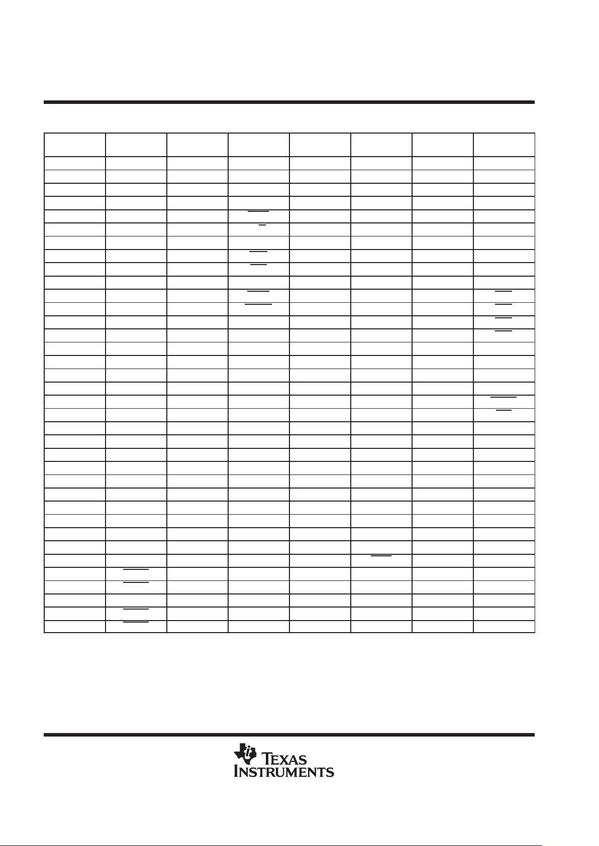
TMS320VC33 Terminal Assignments† (Numerical)
PIN
NUMBER
SIGNAL
NAME
PIN
NUMBER
SIGNAL
NAME
PIN
NUMBER
SIGNAL
NAME
PIN
NUMBER
SIGNAL
NAME
1 A20 37 DV
DD
73 D15 109 CLKX0
2 V
SS
38 H1 74 D14 110 FSX0
3 A19 39 H3 75 D13 111 DX0
4 A18 40 V
SS
76 D12 112 V
SS
5 A17 41 STRB 77 DV
DD
113 TCLK1
6 DV
DD
42 R/W 78 D11 114 TCLK0
7 A16 43 DV
DD
79 D10 115 DV
DD
8 A15 44 IACK 80 V
SS
116 XF1
9 V
SS
45 RDY 81 D9 117 XF0
10 A14 46 CV
DD
82 D8 118 V
SS
11 A13 47 HOLD 83 CV
DD
119 INT3
12 CV
DD
48 HOLDA 84 D7 120 INT2
13 A12 49 V
SS
85 D6 121 INT1
14 A11 50 D31 86 DV
DD
122 INT0
15 DV
DD
51 D30 87 D5 123 CV
DD
16 A10 52 D29 88 D4 124 EDGEMODE
17 A9 53 DV
DD
89 V
SS
125 MCBL/MP
18 V
SS
54 D28 90 D3 126 V
SS
19 A8 55 D27 91 D2 127 RESET
20 A7 56 V
SS
92 D1 128 SHZ
21 A6 57 D26 93 D0 129 DV
DD
22 A5 58 D25 94 DV
DD
130 EXTCLK
23 DV
DD
59 D24 95 EMU1 131 PLLV
DD
‡
24 A4 60 DV
DD
96 EMU0 132 XOUT
25 V
SS
61 D23 97 V
SS
133 XIN
26 A3 62 D22 98 TCK 134 PLLV
SS
‡
27 A2 63 V
SS
99 TDO 135 CLKMD1
28 CV
DD
64 D21 100 TDI 136 CLKMD0
29 A1 65 D20 101 CV
DD
137 CV
DD
30 A0 66 CV
DD
102 TMS 138 RSV1
31 DV
DD
67 D19 103 TRST 139 RSV0
32 PAGE3 68 D18 104 DR0 140 V
SS
33 PAGE2 69 DV
DD
105 V
SS
141 A23
34 V
SS
70 D17 106 FSR0 142 A22
35 PAGE1 71 D16 107 CLKR0 143 DV
DD
36 PAGE0 72 V
SS
108 DV
DD
144 A21
†
DVDD is the power supply for the I/O pins while CVDD is the power supply for the core CPU. VSS is the ground for both the I/O pins and the core
CPU.
‡
PLLVDD and PLLVSS are isolated PLL supply pins that should be externally connected to CVDD and VSS respectively.
PR
O
DU
C
T PREVIEW
Page 5
TMS320VC33
DIGITAL SIGNAL PROCESSOR
SPRS087A – FEBRUARY 1999 – REVISED DECEMBER 1999
5
POST OFFICE BOX 1443 • HOUSTON, TEXAS 77251–1443
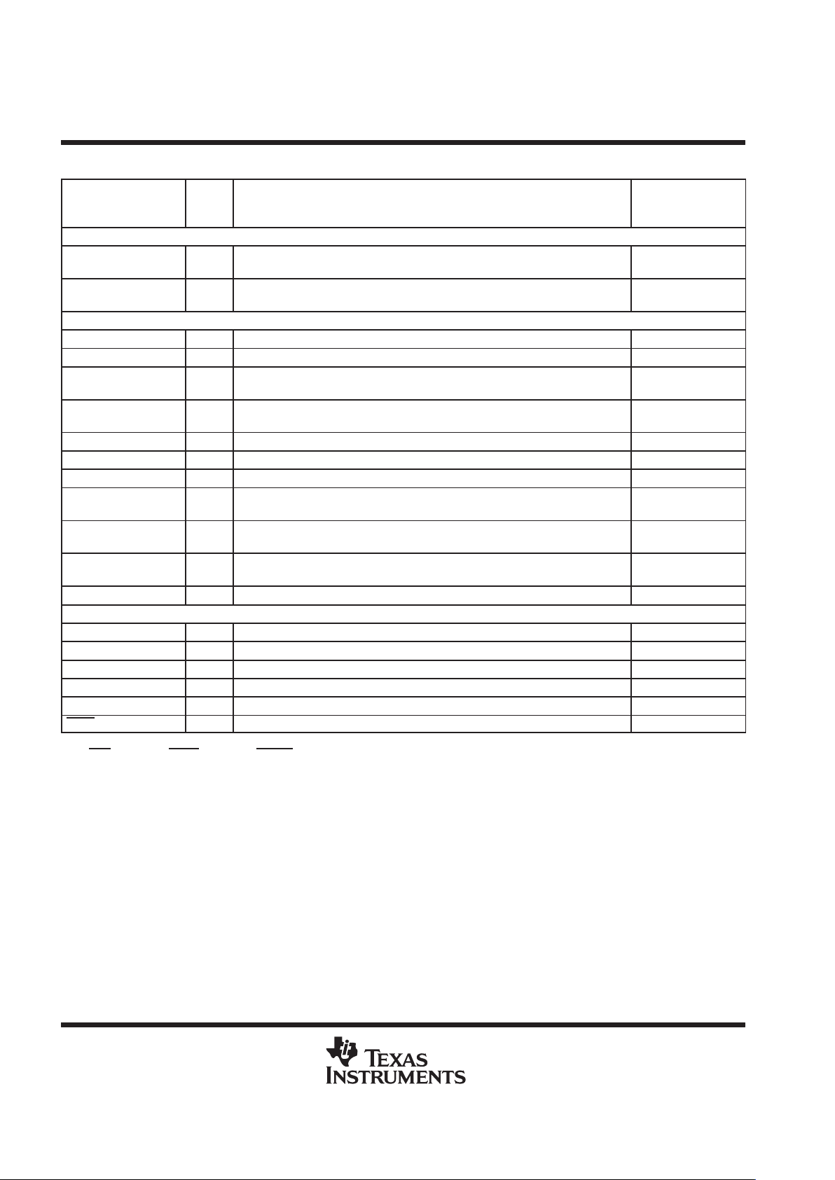
TMS320VC33 Terminal Functions
TERMINAL
CONDITIONS
NAME QTY
TYPE
†
DESCRIPTION
WHEN
SIGNAL IS Z TYPE
‡
PRIMARY-BUS INTERFACE
D31–D0 32 I/O/Z 32-bit data port S H R
A23–A0 24 O/Z 24-bit address port S H R
R/W 1 O/Z
Read/write. R/W is high when a read is performed and low when a write is performed
over the parallel interface.
S H R
STRB 1 O/Z Strobe. For all external-accesses S H
PAGE0 –
PAGE3
1 O/Z Page strobes. Four decoded page strobes for external access S H
RDY 1 I
Ready. RDY indicates that the external device is prepared for a transaction
completion.
HOLD 1 I
Hold. When HOLD is a logic low, any ongoing transaction is completed. A23 –A0,
D31–D0, STRB
, and R/W are placed in the high-impedance state and all
transactions over the primary-bus interface are held until HOLD
becomes a logic high
or until the NOHOLD bit of the primary-bus-control register is set.
HOLDA 1 O/Z
Hold acknowledge. HOLDA is generated in response to a logic low on HOLD.
HOLDA
indicates that A23–A0, D31–D0, STRB, and R/W are in the high-impedance
state and that all transactions over the bus are held. HOLDA
is high in response to
a logic high of HOLD
or the NOHOLD bit of the primary-bus-control register is set.
S
CONTROL SIGNALS
RESET 1 I
Reset. When RESET is a logic low, the device is in the reset condition. When RESET
becomes a logic high, execution begins from the location specified by the reset vec-
tor.
EDGEMODE 1 I Edge mode. Enables interrupt edge mode detection.
INT3–INT0 4 I External interrupts
IACK 1 O/Z
Internal acknowledge. IACK is generated by the IACK instruction. IACK can be used
to indicate when a section of code is being executed.
S
MCBL/MP 1 I Microcomputer Bootloader/microprocessor mode-select
SHZ 1 I
Shutdown high impedance. When active, SHZ places all pins in the high-impedance
state. SHZ
can be used for board-level testing or to ensure that no dual-drive
conditions occur. CAUTION: A low on SHZ
corrupts the device memory and register
contents. Reset the device with SHZ
high to restore it to a known operating condition.
XF1, XF0 2 I/O/Z
External flags. XF1 and XF0 are used as general-purpose I/Os or to support
interlocked processor instruction.
S R
SERIAL PORT 0 SIGNALS
CLKR0 1 I/O/Z Serial port 0 receive clock. CLKR0 is the serial shift clock for the serial port 0 receiver. S R
CLKX0 1 I/O/Z
Serial port 0 transmit clock. CLKX0 is the serial shift clock for the serial port 0
transmitter.
S R
DR0 1 I/O/Z Data-receive. Serial port 0 receives serial data on DR0. S R
DX0 1 I/O/Z Data-transmit output. Serial port 0 transmits serial data on DX0. S R
FSR0 1 I/O/Z
Frame-synchronization pulse for receive. The FSR0 pulse initiates the data-receive
process using DR0.
S R
FSX0 1 I/O/Z
Frame-synchronization pulse for transmit. The FSX0 pulse initiates the data-transmit
process using DX0.
S R
†
I = input, O = output, Z = high-impedance state
‡
S = SHZ
active, H = HOLD active, R = RESET active
§
Recommended decoupling. Four 0.1 µF for V
DDL
and eight 0.1 µF for V
DDP
.
PR
O
DU
C
T PREVIEW
Page 6
TMS320VC33
DIGITAL SIGNAL PROCESSOR
SPRS087A – FEBRUARY 1999 – REVISED DECEMBER 1999
6
POST OFFICE BOX 1443 • HOUSTON, TEXAS 77251–1443
TMS320VC33 Terminal Functions (Continued)
TERMINAL
CONDITIONS
NAME QTY
TYPE
†
DESCRIPTION
WHEN
SIGNAL IS Z TYPE
‡
TIMER SIGNALS
TCLK0 1 I/O/Z
Timer clock 0. As an input, TCLK0 is used by timer 0 to count external pulses. As
an output, TCLK0 outputs pulses generated by timer 0.
S R
TCLK1 1 I/O/Z
Timer clock 1. As an input, TCLK0 is used by timer 1 to count external pulses. As
an output, TCLK1 outputs pulses generated by timer 1.
S R
SUPPLY AND OSCILLATOR SIGNALS
H1 1 O/Z External H1 clock S
H3 1 O/Z External H3 clock S
CV
DD
10 I
+VDD. Dedicated 1.8-V power supply for the core CPU. All must be connected to
a common supply plane.
§
DV
DD
10 I
+VDD. Dedicated 3.3-V power supply for the I/O pins. All must be connected to a
common supply plane.
§
V
SS
24 I Ground. All grounds must be connected to a common ground plane.
PLLV
DD
1 I Internally isolated PLL supply. Connect to CVDD (1.8 V)
PLLV
SS
1 I Internally isolated PLL ground. Connect to V
SS
EXTCLK 1 I
External clock. Logic level compatible clock input. If an oscillator is used, tie this pin
to ground.
XOUT 1 O
Clock out. Output from the internal-crystal oscillator. If a crystal is not used, X1
should be left unconnected.
XIN 1 I
Clock in. Internal-oscillator input from a crystal. If EXTCLK is used, tie this pin to
ground.
RSV0 – RSV1 2 I Reserved. Use individual pullups to DVDD.
JTAG EMULATION
EMU1–EMU0 2 I Emulation pins 0 and 1
TDI 1 I Test data input
TDO 1 O Test data output
TCK 1 I Test clock
TMS 1 I Test mode select
TRST 1 I Test reset
†
I = input, O = output, Z = high-impedance state
‡
S = SHZ
active, H = HOLD active, R = RESET active
§
Recommended decoupling. Four 0.1 µF for V
DDL
and eight 0.1 µF for V
DDP
.
PR
O
DU
C
T PREVIEW
Page 7
TMS320VC33
DIGITAL SIGNAL PROCESSOR
SPRS087A – FEBRUARY 1999 – REVISED DECEMBER 1999
7
POST OFFICE BOX 1443 • HOUSTON, TEXAS 77251–1443
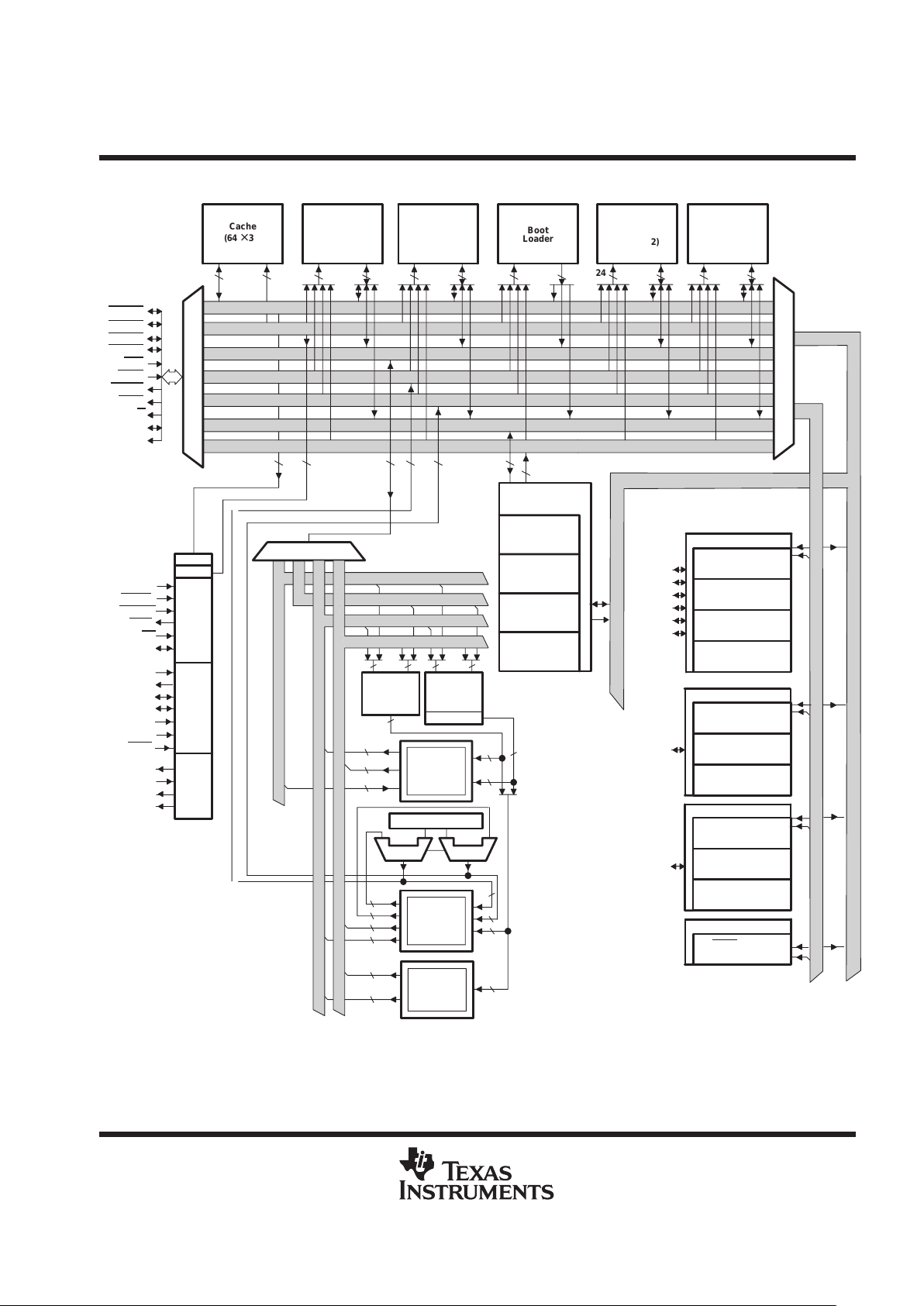
functional block diagram
24
ÉÉÉ
Boot
Loader
Cache
(64
× 32)
RAM
Block 0
(1K
× 32)
RAM
Block 1
(1K
× 32)
RDY
HOLD
HOLDA
STRB
R/W
D31–D0
A23–A0
RESET
CPU1
REG1
REG2
MUX
40
32
32
32
32
32
32
32
24
24
24
24
BK
ARAU0 ARAU1
DISP0, IR0, IR1
Extended-
Precision
Registers
(R7–R0)
Auxiliary
Registers
(AR0–AR7)
Other
Registers
(12)
40
40
40
40
Multiplier
32-Bit
Barrel
Shifter
ALU
DMA Controller
Global-Control
Register
Source-Address
Register
Destination-
Address
Register
Serial Port 0
Serial-Port-Control
Register
Receive/Transmit
(R/X) Timer Register
Data-Transmit
Register
Data-Receive
Register
FSX0
DX0
CLKX0
FSR0
DR0
CLKR0
Timer 0
Global-Control
Register
Timer-Period
Register
Timer-Counter
Register
TCLK0
Timer 1
Global-Control
Register
Timer-Period
Register
Timer-Counter
Register
TCLK1
Port Control
STRB
-Control
Register
Transfer-
Counter
Register
PDATA Bus
PADDR Bus
DDATA Bus
DADDR1 Bus
DADDR2 Bus
DMADATA Bus
DMAADDR Bus
24
40
32
32
24
24
32
INT(3–0)
IACK
MCBL/MP
XF(1,0)
32 24 24
24 2432 32 32
CPU2
32 32 40 40
Peripheral Data Bus
CPU1
REG1
REG2
RAM
Block 2
(16K
× 32)
24
32
RAM
Block 3
(16K
× 32)
24
32
MUX
Peripheral Address Bus
XOUT
XIN
H1
H3
PAGE_0
PAGE_1
PAGE_2
PAGE_3
Peripheral Data Bus
TDI
TDO
TCK
EMU0
EMU1
TMS
TRST
MUX
EDGEMODE
ControllerPLL CLK
JTAG Emulation
IR
PC
PR
O
DU
C
T PREVIEW
Page 8
TMS320VC33
DIGITAL SIGNAL PROCESSOR
SPRS087A – FEBRUARY 1999 – REVISED DECEMBER 1999
8
POST OFFICE BOX 1443 • HOUSTON, TEXAS 77251–1443
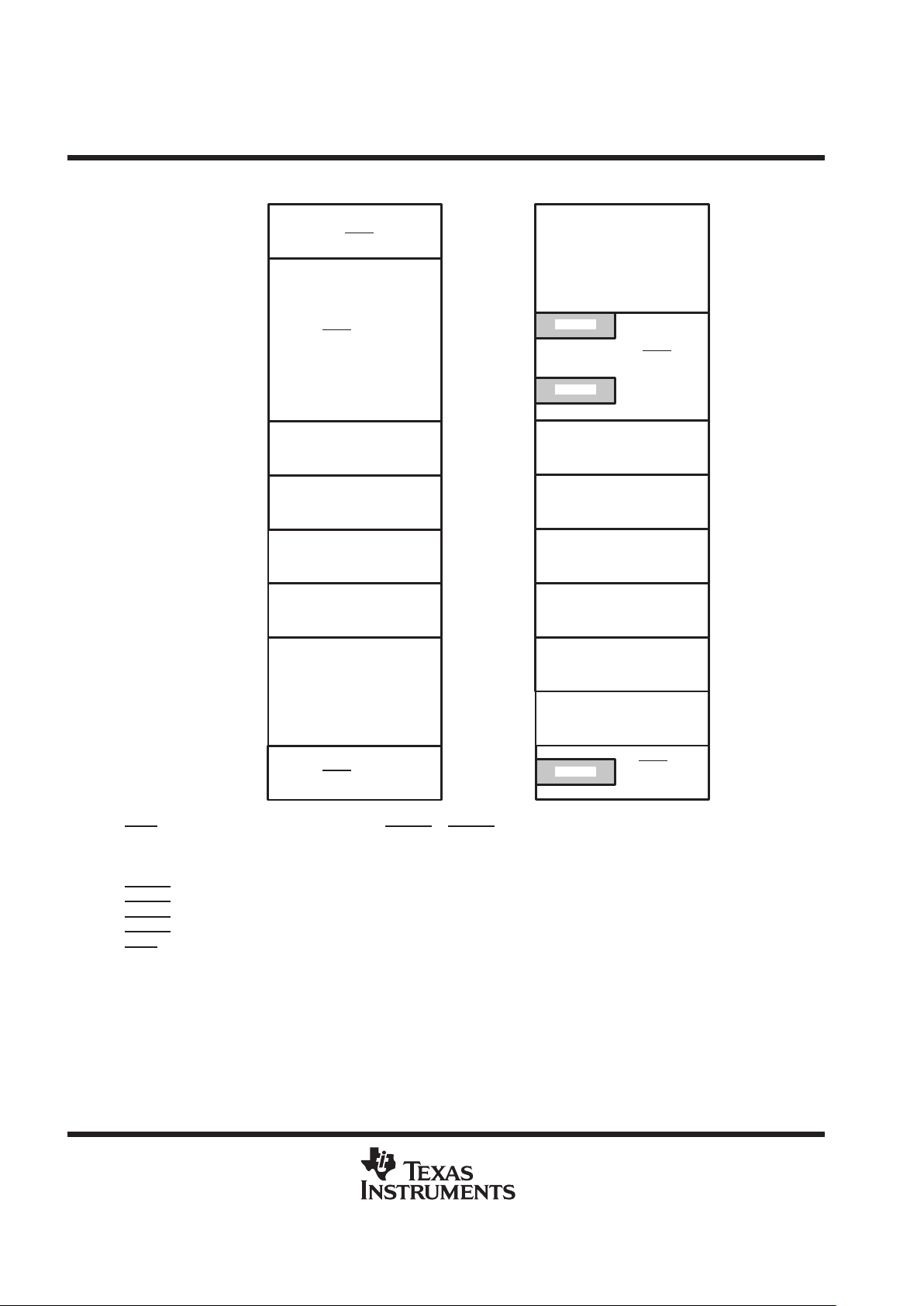
memory map
Peripheral Bus
Memory-Mapped Registers
(6K Words Internal)
Reset, Interrupt, Trap V ector, and
Reserved Locations (64)
(External STRB
Active)
0h
03Fh
040h
External
STRB
Active
(8M Words – 64 Words)
7FFFFFh
800000h
807FFFh
808000h
8097FFh
RAM Block 0
(1K Words Internal)
809800h
809BFFh
809C00h
809FFFh
80A000h
External
STRB
Active
(8M Words – 40K Words)
FFFFFFh
0h
FFFh
1000h
7FFFFFh
800000h
807FFFh
Peripheral Bus
Memory-Mapped Registers
(6K Words Internal)
808000h
8097FFh
RAM Block 0
(1K Words Internal)
809800h
809BFFh
809C00h
809FFFh
80A000h
External
STRB
Active
(8M Words –
40K Words)
FFFFFFh
Boot 1
Boot 2
400000h
RAM Block 1
(1K Words – 63 Words Internal)
809FC0h
809FC1h
User-Program Interrupt
and Trap Branches
(63 Words Internal)
Boot 3
FFF000h
External
STRB
Active
(8M Words –
4K Words)
Reserved for Bootloader
Operations
(a) Microprocessor Mode
(b) Microcomputer/Bootloader Mode
RAM Block 1
(1K Words Internal)
RAM Block 3
(16K Words Internal)
RAM Block 2
(16K Words Internal)
RAM Block 3
(16K Words Internal)
RAM Block 2
(16K Words Internal)
803FFFh
804000h
803FFFh
804000h
NOTE A: STRB is active over all external memory ranges. PAGE_0 to PAGE_3 are configured as external bus strobes. These are simple
decoded strobes that have no configuration registers and are active only during external bus activity over the following ranges:
Name Active range
PAGE_0
0000000h – 03FFFFFh
PAGE_1
0400000h – 07FFFFFh
PAGE_2
0800000h – 0BFFFFFh
PAGE_3
0C00000h – 0FFFFFFh
STRB
0000000h – 0FFFFFFh
Figure 1. TMS320C33 Memory Maps
PR
O
DU
C
T PREVIEW
Page 9
TMS320VC33
DIGITAL SIGNAL PROCESSOR
SPRS087A – FEBRUARY 1999 – REVISED DECEMBER 1999
9
POST OFFICE BOX 1443 • HOUSTON, TEXAS 77251–1443
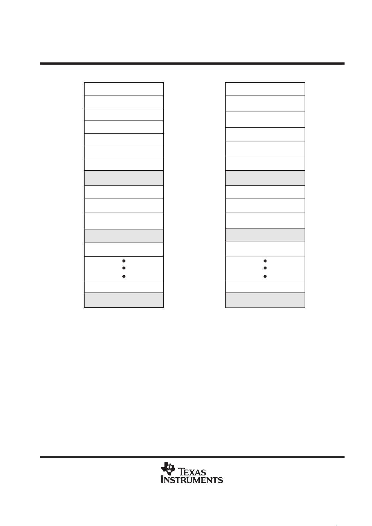
memory map (continued)
Reset
00h
INT0
809FC1h
INT1
01h
INT1
809FC2h
INT2
02h
INT2
809FC3h
INT3
03h
INT3
809FC4h
XINT0
04h
XINT0
809FC5h
RINT0
06h
RINT0
809FC6h
07h
809FC7h
809FC8h
08h
TINT0
09h
809FC9h
TINT1
0Ah
809FCAh
DINT
0Bh
809FCBh
0Ch
809FDFh
1Fh
809FCCh
TRAP 020h
809FE0h
TRAP 273Bh 809FFBh
3Ch
809FFFh
3Fh
809FFCh
(a) Microprocessor Mode (b) Microcomputer/Bootloader Mode
INT0
05h
TINT0
TRAP 27
TRAP 0
DINT
TINT1
Reserved
Reserved
Reserved
Reserved
Reserved
Reserved
Figure 2. Reset, Interrupt, and Trap Vector/Branches Memory-Map Locations
PR
O
DU
C
T PREVIEW
Page 10
TMS320VC33
DIGITAL SIGNAL PROCESSOR
SPRS087A – FEBRUARY 1999 – REVISED DECEMBER 1999
10
POST OFFICE BOX 1443 • HOUSTON, TEXAS 77251–1443
memory map (continued)
FSX/DX/CLKX Serial Port Control
FSR/DR/CLKR Serial Port Control
Serial R/X Timer Control
Serial R/X Timer Counter
Serial R/X Timer Period Register
Data-Transmit
Data-Receive
Primary-Bus Control
DMA Global Control
DMA Source Address
DMA Destination Address
DMA Transfer Counter
Timer 0 Global Control
Timer 0 Counter
Timer 0 Period Register
Timer 1 Global Control
Timer 1 Counter
Timer 1 Period Register
Serial Global Control
808000h
808004h
808006h
808008h
808020h
808024h
808028h
808030h
808034h
808038h
808040h
808042h
808043h
808044h
808045h
808046h
808048h
80804Ch
808064h
NOTE A: Shading denotes reserved address locations.
Figure 3. Peripheral Bus Memory-Mapped Registers
clock generator
The clock generator provides clocks to the ’VC33 device, and consists of an internal oscillator and a
phase-locked loop (PLL) circuit. The clock generator requires a reference clock input, which can be provided
by using a crystal resonator with the internal oscillator, or from an external clock source. The PLL circuit
generates the device clock by multiplying the reference clock frequency by a scale factor, allowing use of a clock
source with a lower frequency than that of the CPU.The PLL is an adaptive circuit that, once synchronized, locks
onto and tracks an input clock signal.
PR
O
DU
C
T PREVIEW
Page 11
TMS320VC33
DIGITAL SIGNAL PROCESSOR
SPRS087A – FEBRUARY 1999 – REVISED DECEMBER 1999
11
POST OFFICE BOX 1443 • HOUSTON, TEXAS 77251–1443
PLL and clock oscillator control
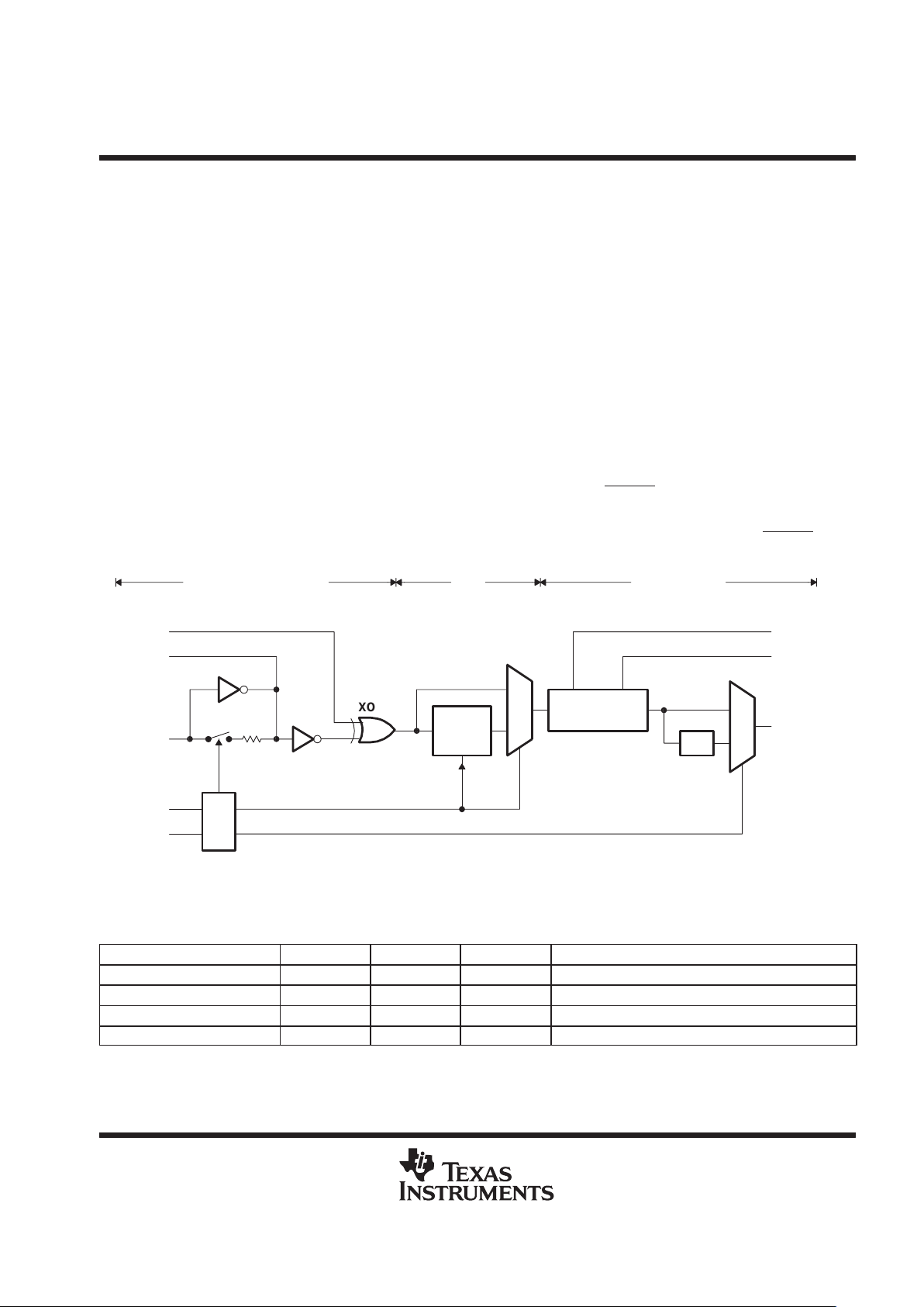
The clock mode control pins are decoded into four operational modes as shown in Figure 4. These modes
control clock divide ratios, oscillator, and PLL power (see Table 1).
When an external clock input or crystal is connected, the opposite unused input is simply grounded. An XOR
gate then passes one of the two signal sources to the PLL stage. This allows the direct injection of a clock
reference into EXTCLK, or 1–20 MHz crystals and ceramic resonators with the oscillator circuit. The two clock
sources include:
D A crystal oscillator circuit, where a crystal or ceramic resonator is connected across the XOUT and XIN pins
and EXTCLK is grounded.
D An external clock input, where an external clock source is directly connected to the EXTCLK pin, and XOUT
is left unconnected and XIN is grounded.
When the PLL is initially started, it enters a transitional mode during which the PLL acquires lock with the input
signal. Once the PLL is locked, it continues to track and maintain synchronization with the input signal. The PLL
is a simple x5 reference multiplier with bypass and power control.
The clock divider, under CPU control, reduces the clock reference by 1 (MAXSPEED), 1/16 (LOWPOWER), or
clock stop (IDLE2). Wakeup from the IDLE2 state is accomplished by a RESET or interrupt pin logic low state.
A divide-by-two TMS320C31 equivalent mode of operation is also provided. In this case, the clock output
reference is further divided by two with clock synchronization being determined by the timing of RESET falling
relative to the present H1/H3 state.
Clock DividerPLLClock & Crystal OSC
CLKMD1
CLKMD0
PLL PWR and Bypass
Oscillator Enable
C31 DIV2 Mode
LOWPOWER
MAXSPEED/
IDLE2
H1 CLK
1/2
U
M
X
X1, 1/16, Off
XOR
SEL
X
U
M
PLLX5
EXTCLK
XIN
XOUT
RFS1
Figure 4. Clock Generation
Table 1. Clock Mode Select Pins
CLKMD0 CLKMD1 FEEDBACK PLLPWR RATIO NOTES
0 0 Off Off 1 Fully static, very low power
0 1 On Off 1/2 Oscillator enabled
1 0 On Off 1 Oscillator enabled
1 1 On On 5 10 mA @ 1.8 V PLL power. Oscillator enabled
PR
O
DU
C
T PREVIEW
Page 12
TMS320VC33
DIGITAL SIGNAL PROCESSOR
SPRS087A – FEBRUARY 1999 – REVISED DECEMBER 1999
12
POST OFFICE BOX 1443 • HOUSTON, TEXAS 77251–1443
PLL and clock oscillator control (continued)
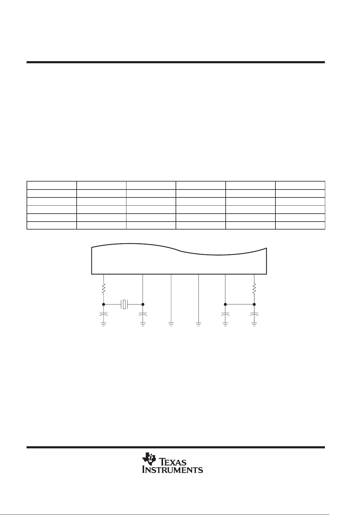
Typical crystals in the 8 – 30 MHz range have a series resistance of 25 Ω which increases below 8 MHz. To
maintain proper filtering and phase relationships, R
d
and Z
out
of the oscillator circuit should be 10x – 40x that
of the crystal. A series compensation resistor (Rd), shown in Figure 5, is recommended when using lower
frequency crystals. The XOUT output, the square wave inverse of XIN, is then filtered by the XOUT output
impedance, C1 load capacitor, and R
d
(if present). The crystal and C2 input load capacitor then refilters this
signal resulting in a XIN signal that is 30 – 80% of the oscillator supply voltage.
NOTE: Some ceramic resonators are available in a low-cost, three-terminal package that includes C1 and C2
internally. Typically ceramic resonators do not provide the frequency accuracy of crystals.
NOTE: Better PLL stability can be achieved using the optional power supply isolation circuit shown in Figure 5.
A similar filter can be used to isolate the PLLV
SS
, as shown in Figure 6. PLLVDD can also be directly connected
to CVDD.
Table 2. Typical Crystal Circuit Loading
FREQUENCY (MHz) Rd (Ω) C1 (pF) C2 (pF) CL† (pF) RL† (Ω)
2 4.7K 18 18 12 200
5 2.2K 18 18 12 60
10 470 15 15 12 30
15 0 15 12 12 25
20 0 9 9 10 25
†
CL and RL are typical internal series load capacitance and resistance of the crystal.
XOUT XIN
C1 C2
Crystal
EXTCLKRdPLLV
SS
CV
DD
100 Ω
PLLV
DD
0.1 µF
0.01 µF
Figure 5. Self-Oscillation Mode
PR
O
DU
C
T PREVIEW
Page 13
TMS320VC33
DIGITAL SIGNAL PROCESSOR
SPRS087A – FEBRUARY 1999 – REVISED DECEMBER 1999
13
POST OFFICE BOX 1443 • HOUSTON, TEXAS 77251–1443
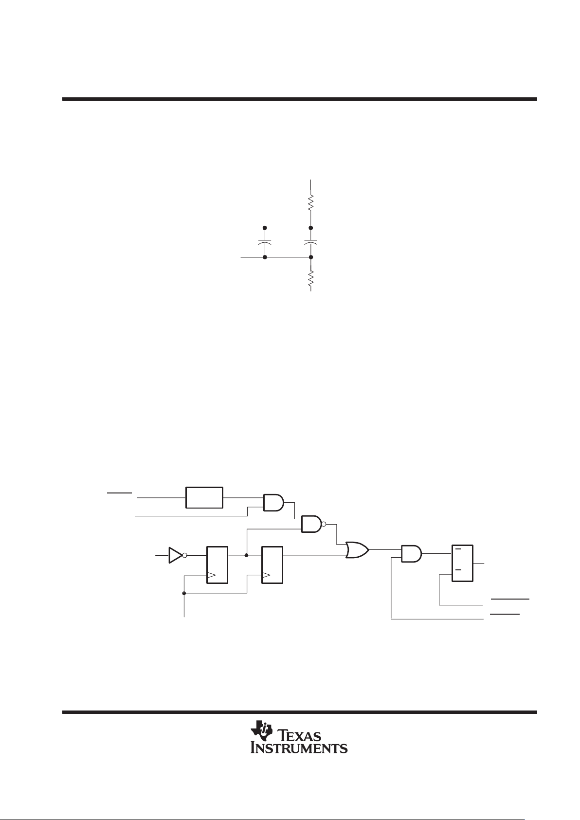
PLL isolation
The internal PLL supplies can be directly connected to CV
DD
and VSS (0 Ω case) or fully isolated as shown in
Figure 6. The RC network prevents the PLL supplies from turning high frequency noise in the CVDD and V
SS
supplies into jitter.
CV
DD
0 –100 Ω
0.1 µF
0.01 µF
0 –100 Ω
V
SS
PLLV
DD
PLLV
SS
Figure 6. PLL Isolation Circuit Diagram
EDGEMODE
When EDGEMODE = 1 a sampled digital delay line is decoded to generate a pulse on the falling edge of the
interrupt pin. T o guarantee interrupt recognition, input signal logic high and logic low states must be held longer
than the synchronizer delay of one CPU clock cycle. Holding these inputs to no less than two cycles in both the
logic low and logic high states is sufficient.
When EDGEMODE = 0, a logic low interrupt pin will continually set the corresponding interrupt flag. The CPU
or DMA can clear this flag within two cycles of it being set. This is the maximum interrupt width that can be applied
if only one interrupt is to be recognized. The CPU can manually clear IF bits within an ISR, effectively lengthening
the maximum ISR width.
After reset, EDGEMODE is temporarily disabled allowing logic low INT pins to be detected for bootload
operation.
CPU Set
IF Bit
RESET
EDGEMODE
CPU Reset
INTn
H1
Delay
DDQQ
Q
R
S
Figure 7. EDGEMODE and Interrupt Flag CIrcuit
PR
O
DU
C
T PREVIEW
Page 14

TMS320VC33
DIGITAL SIGNAL PROCESSOR
SPRS087A – FEBRUARY 1999 – REVISED DECEMBER 1999
14
POST OFFICE BOX 1443 • HOUSTON, TEXAS 77251–1443
reset operation
When RESET
is applied, the CPU attempts to safely exit any pending read or write operations that may be in
progress. This can take as much as 10 CPU cycles, after which, the address, data, and control pins will be in
a high-impedance state.
When both RESET and SHZ are applied, the device will immediately enter the reset state with the pins held in
high impedance mode. SHZ
should then be disabled at least 10 CPU cycles before RESET is set high. SHZ
can be used during power-up sequencing to prevent undefined address, data, and control pins, avoiding system
conflicts.
PAGE0 – PAGE3 select lines
To facilitate simpler and higher speed connection to external devices, the TMS320VC33 includes four
predecoded select pins that have the same timings as STRB. These pins are decoded from A22, A23, and STRB
and are active only during external accesses over the ranges shown in Table 3. All external bus accesses are
controlled by a single bus control register.
T able 3. PAGE0 – PAGE3 Ranges
START END
PAGE0 0x000000 0x3FFFFF
PAGE1 0x400000 0x7FFFFF
PAGE2 0x800000 0xBFFFFF
PAGE3 0xC00000 0xFFFFFF
PR
O
DU
C
T PREVIEW
Page 15
TMS320VC33
DIGITAL SIGNAL PROCESSOR
SPRS087A – FEBRUARY 1999 – REVISED DECEMBER 1999
15
POST OFFICE BOX 1443 • HOUSTON, TEXAS 77251–1443
boot loader operation
When MCBL/MP = 0, an internal ROM is decoded into the address range of 0x000000–0x001000. Therefore,
when reset occurs, execution begins within the internal ROM program and vector space. No external activity
will be evident until one of the boot options is enabled. These options are enabled by pulling an external interrupt
pin low, which the boot load software then detects, causing a particular routine to be executed (see Table 4).
Table 4. INT0 – INT3 Sources
ACTIVE INTERRUPT
ADDRESS/SOURCE WHERE BOOT DATA IS
READ FROM
DATA FORMAT
INT0 0x001000 8, 16, or 32-bit width
INT1 0x400000 8, 16, or 32-bit width
INT2 0xFFF000 8, 16, or 32-bit width
INT3 Serial Port 32-bit, external clock, and frame synch
When MCBL/MP = 0, the reset and interrupt vectors are hard coded within the internal ROM. Since this is a
read-only device, these vectors cannot be modified. To enable user defined interrupt routines, the internal
vectors contain fixed values that point to an internal section of SRAM beginning at 0x809FC1. Code execution
begins at these locations so it is important to place branch instructions (to the interrupt routine) at these locations
and not vectors.
The bootloader program requires a small stack space for calls and returns. Two SRAM locations a 0x809800
and 0x809801 are used for this stack. Y ou should not try to bootload data into these locations as it will corrupt
the boot loader program run time stack. After the bootload operation is complete, your program can reclaim
these locations. The simplest solution is to begin your programs uninitialized data section at this location.
For additional detail on boot loader operation including the boot loader source code, see the
TMS320C3x Users
Guide
(literature number SPRU031).
PR
O
DU
C
T PREVIEW
Page 16

TMS320VC33
DIGITAL SIGNAL PROCESSOR
SPRS087A – FEBRUARY 1999 – REVISED DECEMBER 1999
16
POST OFFICE BOX 1443 • HOUSTON, TEXAS 77251–1443
absolute maximum ratings over specified temperature range (unless otherwise noted)
†
Supply voltage range, DV
DD
(see Note 1) –0.3 V to 4 V. . . . . . . . . . . . . . . . . . . . . . . . . . . . . . . . . . . . . . . . . . . .
Supply voltage range, CV
DD
(see Note 1) –0.3 V to 2 V. . . . . . . . . . . . . . . . . . . . . . . . . . . . . . . . . . . . . . . . . . . .
Input voltage range, VI –0.3 V to 4.5 V. . . . . . . . . . . . . . . . . . . . . . . . . . . . . . . . . . . . . . . . . . . . . . . . . . . . . . . . . . .
Output voltage range, V
O
–0.3 V to 4.5 V. . . . . . . . . . . . . . . . . . . . . . . . . . . . . . . . . . . . . . . . . . . . . . . . . . . . . . . .
Continuous power dissipation (worst case) (see Note 2) 500 mW. . . . . . . . . . . . . . . . . . . . . . . . . . . . . . . . . . .
(for TMS320VC33-150)
Operating case temperature range, T
C
PQL (commercial) 0°C to 85°C. . . . . . . . . . . . . . . . . . . . . . . . . . . .
PQA (industrial) – 40°C to 125°C. . . . . . . . . . . . . . . . . . . . . . . . . .
Storage temperature range, T
stg
– 55°C to 150°C. . . . . . . . . . . . . . . . . . . . . . . . . . . . . . . . . . . . . . . . . . . . . . . . .
†
Stresses beyond those listed under “absolute maximum ratings” may cause permanent damage to the device. These are stress ratings only, and
functional operation of the device at these or any other conditions beyond those indicated under “recommended operating conditions” is not
implied. Exposure to absolute-maximum-rated conditions for extended periods may affect device reliability.
NOTES: 1. All voltage values are with respect to VSS.
2. Actual operating power is much lower. This value was obtained under specially produced worst-case test conditions for the
TMS320VC33, which are not sustained during normal device operation. These conditions consist of continuous parallel writes of
a checkerboard pattern to the external data and address buses at the maximum possible rate with a capacitive load of 30 pF . See
normal (ICC) current specification in the electrical characteristics table and also read
Calculation of TMS320C30 Power Dissipation
Application Report
(literature number SPRA020)
.
recommended operating conditions (see Note 3 and Note 4)
MIN NOM MAX UNIT
CV
DD
Supply voltage for the core CPU 1.71 1.8 1.89 V
DV
DD
Supply voltage for the I/O pins 3 3.3 3.6 V
V
SS
Supply ground 0 V
V
IH
High-level input voltage 0.7 * DV
DD
DVDD + 0.3 V
V
IL
Low-level input voltage – 0.3
‡
0.3 * DV
DD
V
I
OH
High-level output current 4 mA
I
OL
Low-level output current 4 mA
Operating case temperature (commercial) 0 85
T
C
Operating case temperature (industrial)
°C
C
L
Capacitive load per output pin 30 pF
NOTES: 3. All voltage values are with respect to VSS. EXTCLK can be driven by a CMOS clock.
4. All inputs and I/O pins configured as inputs, except SHZ
and D0–D31, use Schmidt hysteresis inputs. Hysteresis is approximately
10% of DVDD and is centered at 0.5 * DVDD.
PR
O
DU
C
T PREVIEW
Page 17

TMS320VC33
DIGITAL SIGNAL PROCESSOR
SPRS087A – FEBRUARY 1999 – REVISED DECEMBER 1999
17
POST OFFICE BOX 1443 • HOUSTON, TEXAS 77251–1443
electrical characteristics over recommended ranges of supply voltage (unless otherwise noted)
(see Note 3)
†
PARAMETER TEST CONDITIONS MIN TYP‡MAX UNIT
V
OH
High-level output voltage VDD = MIN, IOH = MAX 2.4 V
V
OL
Low-level output voltage VDD = MIN, IOH = MAX 0.4 V
I
Z
High-impedance current VDD = MAX – 5 + 5 µA
I
I
Input current VI = VSS to V
DD
– 5 + 5 µA
I
IPU
Input current (with internal pullup) Inputs with internal pullups
§
– 600 10 µA
I
IPD
Input current (with internal pulldown) Inputs with internal pulldowns 600 – 10 µA
I
BKU
Input current (with bus keeper) pullup
¶
Bus keeper opposes until conditions match – 600 10 µA
I
BKD
Input current (with bus keeper) pulldown
¶
600 – 10 µA
T
= 25°C,
fx = 60 MHz ’VC33-120 20 120
I
DDD
Supply current, pins
#||
T
A
=
25 C
,
DVDD = MAX
fx = 75 MHz ’VC33-150 25 150
mA
T
= 25°C,
fx = 60 MHz ’VC33-120 40 50
I
DDC
Supply current, core CPU
#||
T
A
=
25 C
,
CVDD = MAX
fx = 75 MHz ’VC33-150 45 60
mA
PLL enabled, oscillator enabled 10 mA
I
DD
IDLE2, Supply current, I
DDD
plus I
DDC
PLL disabled, oscillator enabled 500
IDDIDLE2, Su ly current, I
DDD
lus I
DDC
PLL disabled, oscillator disabled, FCLK = 0 50
µA
All inputs except XIN 10
C
i
Input capacitance
XIN
10
pF
C
o
Output capacitance 10 pF
†
All input and output voltage levels are TTL compatible.
‡
For ’VC33, all typical values are at DVDD = 3.3, CVDD = 1.8 V, TA (air temperature) = 25°C.
§
Pins with internal pullup devices: TDI, TCK, and TMS. Pin with internal pulldown device: TRST
.
¶
Pins D0–D31 include internal bus keepers to maintain valid logic levels when the bus is not driven.
#
Actual operating current is less than this maximum value. This value was obtained under specially produced worst-case test conditions, which
are not sustained during normal device operation. These conditions consist of continuous parallel writes of a checkerboard pattern at the
maximum rate possible. See
Calculation of TMS320C30 Power Dissipation Application Report
(literature number SPRA020).
||
fx is the PLL output clock frequency.
NOTE 3: All voltage values are with respect to VSS. EXTCLK can be driven by a CMOS clock.
PARAMETER MEASUREMENT INFORMATION
Tester Pin
Electronics
V
Load
I
OL
C
T
I
OH
Output
Under
Test
Where: I
OL
= 4 mA (all outputs)
I
OH
= 4 mA (all outputs)
V
LOAD
=DVDD/2
C
T
= 30-pF typical load-circuit capacitance
Figure 8. TMS320VC33 Test Load Circuit
PR
O
DU
C
T PREVIEW
Page 18

TMS320VC33
DIGITAL SIGNAL PROCESSOR
SPRS087A – FEBRUARY 1999 – REVISED DECEMBER 1999
18
POST OFFICE BOX 1443 • HOUSTON, TEXAS 77251–1443
PARAMETER MEASUREMENT INFORMATION
timing parameter symbology
Timing parameter symbols used herein were created in accordance with JEDEC Standard 100-A. In order to
shorten the symbols, some of the pin names and other related terminology have been abbreviated as follows,
unless otherwise noted:
A A23–A0 H H1 and H3
ASYNCH Asynchronous reset signals HOLD HOLD
C CLKX0 HOLDA HOLDA
CI CLKIN IACK IACK
CLKR CLKR0 INT INT3–INT0
CONTROL Control signals PAGE P AGE0–PAGE3
D D31–D0 RDY RDY
DR DR RW R/W
DX DX RESET RESET
FS FSX/R S STRB
FSX FSX0 SCK CLKX/R
FSR FSR0 SHZ SHZ
GPI General-purpose input TCLK TCLK0, TCLK1, or TCLKx
GPIO General-purpose input/output; peripheral pin XF XF0, XF1, or XFx
GPO General-purpose output XFIO XFx switching from input to output
PR
O
DU
C
T PREVIEW
Page 19

TMS320VC33
DIGITAL SIGNAL PROCESSOR
SPRS087A – FEBRUARY 1999 – REVISED DECEMBER 1999
19
POST OFFICE BOX 1443 • HOUSTON, TEXAS 77251–1443
timing
Timing specifications apply to the TMS320VC33.
EXTCLK, H1, and H3 timing
The following table defines the timing parameters for the EXTCLK, H1, and H3 interface signals. The numbers
shown in Figure 9 and Figure 10 correspond with those in the number (NO.) column of the table below.
timing parameters for EXTCLK, H1, and H3 in ’C31 divide-by-2 mode† (see Figure 9 and Figure 10)
’VC33-120 ’VC33-150
NO.
MIN MAX MIN MAX
UNIT
1 t
f(CI)
Fall time, CLKIN 1 1 ns
2 t
w(CIL)
Pulse duration, CLKIN low t
c(CI)
= min (time below VIL) 4 4 ns
3 t
w(CIH)
Pulse duration, CLKIN high t
c(CI)
= min (time above VIH) 4 4 ns
4 t
r(CI)
Rise time, CLKIN 1 1 ns
5 t
c(CI)
Cycle time, CLKIN 10 10 ns
6 t
f(H)
Fall time, H1 and H3 3 3 ns
7 t
w(HL)
Pulse duration, H1 and H3 low t
c(CL)
– 2 t
c(CL)
+ 2 t
c(CL)
– 2 t
c(CL)
+ 2 ns
8 t
w(HH)
Pulse duration, H1 and H3 high t
c(CL)
– 2 t
c(CL)
+ 2 t
c(CL)
– 2 t
c(CL)
+ 2 ns
9 t
r(H)
Rise time, H1 and H3 3 3 ns
10 t
d(HL-HH)
Delay time. from H1 low to H3 high or from H3 low to H1 high –1.5 1.5 –1.5 1.5 ns
11 t
c(H)
Cycle time, H1 and H3 2 * t
c(CL)
2 * t
c(CL)
ns
†
Similar loading characteristics must be used on all pins.
1
4
EXTCLK
5
2
3
Figure 9. Timing for EXTCLK
H3
H1
6
9
10
10
6
9
11
7
7
8
11
8
Figure 10. Timing for H1 and H3
PR
O
DU
C
T PREVIEW
Page 20

TMS320VC33
DIGITAL SIGNAL PROCESSOR
SPRS087A – FEBRUARY 1999 – REVISED DECEMBER 1999
20
POST OFFICE BOX 1443 • HOUSTON, TEXAS 77251–1443
clock circuit timing
The following table defines the timing parameters for the clock circuit signals.
timing and circuit parameters for on-chip crystal oscillator† (see Figure 11)
MIN TYP MAX UNIT
V
O
Oscillator internal supply voltage CV
DD
V
F
O
Fundamental mode frequency range 5 20 MHz
V
bias
DC bias point (input threshold) 40 50 60 %V
O
R
fbk
Feedback resistance 100 300 500 KΩ
R
out
Small signal AC output impedance 250 500 1000 Ω
V
xoutac
AC output voltage with test crystal
‡
80 %V
O
V
xinac
AC input voltage with test crystal
‡
50 %V
O
V
xoutl
V
xin
= V
xinh
, I
xout
= 0, FO=0 (logic input) VSS – 0.1 VSS + 0.3 V
V
xouth
V
xin
= V
xinl
, I
xout
= 0, FO=0 (logic input) CVDD – 0.3 CVDD + 0.1 V
V
inl
When used for logic level input, oscillator enabled –0.3 0.2 * V
O
V
V
inh
When used for logic level input, oscillator enabled 0.8 * V
O
DVDD + 0.3 V
V
xinh
When used for logic level input, oscillator disabled 0.7 * DV
DD
DVDD + 0.3 V
C
xout
XOUT internal load capacitance 2 3 5 pF
C
xin
XIN internal load capacitance 2 3 5 pF
t
d(XIN-H1)
Delay time, XIN to H1 x1 and x0.5 modes 9 12 ns
I
inl
Input current, feedback enabled, Vil = 0 50 µA
I
inh
Input current, feedback enabled, Vil = V
ih
–50 µA
†
This circuit is intended for fundamental mode operation.
‡
Signal amplitude is dependent on the crystal and load used.
XOUT
XIN
C
1
C
2
Crystal
R
fbk
Rd
V
O
C
XIN
C
XOUT
R
OUT
To internal
clock generator
Figure 11. On-Chip Oscillator Circuit
PR
O
DU
C
T PREVIEW
Page 21

TMS320VC33
DIGITAL SIGNAL PROCESSOR
SPRS087A – FEBRUARY 1999 – REVISED DECEMBER 1999
21
POST OFFICE BOX 1443 • HOUSTON, TEXAS 77251–1443
clock circuit timing (continued)
The following table defines the timing parameters for EXTCLK.
timing and circuit parameters for EXTCLK, all modes (see Figure 12 and Figure 13)
NO. MIN TYP MAX UNIT
x5 mode 5 12
Frequency range, 1/t
c(H
)
, ’VC33-120
x1 mode 0 60
Frequency range, 1/t
c(H)
, VC33 120
x0.5 mode 0 100
5a F
ext
x5 mode 5 15
MHz
Frequency range, 1/t
c
(H)
, ’VC33-150
x1 mode 0 75
Frequency range, 1/t
c(H)
, VC33 150
x1 mode 0 100
V
mid
Mid level, used to measure duty cycle 0.5 * DV
DD
V
F=F
max
, x0.5 and x1 mode 1
4 T
r
Rise time
F<F
max
4
ns
F=F
max
, x0.5 and x1 mode 1
1 T
r
Fall time
F<F
max
4
ns
x5 mode 21
2 T
lo
Vil pulse time
x1 mode
5.5
ns
2
TloV
il
ulse time
x0.5 mode 4.0
ns
x5 mode 21
3 T
hi
Vih pulse time
x1 mode
5.5
ns
3
ThiV
ih
ulse time
x0.5 mode 4.0
ns
x5 PLL mode 40 60
5b EXTCLKDC Input duty cycle
x1 and x0.5 mode, F=max
45 55
%
5b
EXTCLKDC
In ut duty cycle
x1 and x0.5 mode, F=0 Hz 0 100
%
x1 mode 7 10
10b td
(EXTCLK-H1)
Delay time, EXTCLK to H1
x0.5 mode 9 12
ns
phase-locked loop characteristics using EXTCLK or on-chip crystal oscillator
†
MIN TYP MAX UNIT
F
pllin
Frequency range, PLL input 5 15 MHz
F
pllout
Frequency range, PLL output 25 75 MHz
I
pll
PLL current, CVDD supply 10 mA
P
pll
PLL power, CVDD supply 20 mW
PLL
dc
PLL output duty cycle at H1 45 55 %
PLLJ PLL output jitter, F
pllout
= 25 MHz 100 pS
†
Duty cycle is defined as 100*t1/(t1+t2)%
PR
O
DU
C
T PREVIEW
Page 22

TMS320VC33
DIGITAL SIGNAL PROCESSOR
SPRS087A – FEBRUARY 1999 – REVISED DECEMBER 1999
22
POST OFFICE BOX 1443 • HOUSTON, TEXAS 77251–1443
clock circuit timing (continued)
T o ensure clean internal clock references, the minimal low and high pulse duration must be maintained. At high
frequencies this may require a fast rise and fall time as well as a tightly controlled duty cycle. At lower frequencies
these requirements are less restrictive when in x1 and x0.5 modes. The PLL, however, must have an input duty
cycle of between 40% and 60% for proper operation.
H3
H1
EXTCLK
10b
5a
10b
1
2
4
3
Figure 12. Divide-By-Two Mode
H3
H1
EXTCLK
10b
5a
10b
1
2
4
3
Figure 13. Divide-By-One Mode
PR
O
DU
C
T PREVIEW
Page 23

TMS320VC33
DIGITAL SIGNAL PROCESSOR
SPRS087A – FEBRUARY 1999 – REVISED DECEMBER 1999
23
POST OFFICE BOX 1443 • HOUSTON, TEXAS 77251–1443
memory read/write timing
The following table defines memory read/write timing parameters for STRB
. The numbers shown in Figure 15
and Figure 16 correspond with those in the NO. column of the table below.
timing parameters for memory (STRB = 0) read/write† (see Figure 14, Figure 15, and Figure 16)
’VC33-120 ’VC33-150
NO.
MIN MAX MIN MAX
UNIT
12 t
d(H1L-SL)
Delay time, H1 low to STRB low 0 4 0 3 ns
13 t
d(H1L-SH)
Delay time, H1 low to STRB high 0 4 0 3 ns
14 t
d(H1H-RWL)R
Delay time, H1 high to R/W low (read) 0 4 0 3 ns
15 t
d(H1L-A)
Delay time, H1 low to A valid 0 4 0 3 ns
16 t
su(D-H1L)R
Setup time, D before H1 low (read) 6 5 ns
17 t
h(H1L-D)R
Hold time, D after H1 low (read) 1 1 ns
18 t
su(RDY-H1H)
Setup time, RDY before H1 high 5 4 ns
19 t
h(H1H-RDY)
Hold time, RDY after H1 high 0 0 ns
20 t
d(H1H-RWH)W
Delay time, H1 high to R/W high (write) 4 3 ns
21 t
v(H1L-D)W
Valid time, D after H1 low (write) 7 6 ns
22 t
h(H1H-D)W
Hold time, D after H1 high (write) 0 7 0 6 ns
23 t
d(H1H-A)W
Delay time, H1 high to A valid on back-to-back write cycles (write) 4 3 ns
24 t
d(A-RDY)
Delay time, RDY from A valid P–6
‡
P–5
‡
ns
24A T
aa
Address valid to data valid (read), 0 wait state, CL = 30 pF 9 6 ns
24B T
aa
Address valid to data valid (read), 1 wait state 24.6 19.3 ns
†
These timings assume a similar loading of 30 pF on all pins.
‡
P = t
c(CL)
Output load characteristics for high-speed and low-speed (low-noise) output buffers are shown in Figure 14.
High-speed buffers are used on A0 – A23, P AGE0 – P AGE3, H1, H3, STRB, and R/W . All other outputs use the
low-speed, (low-noise) output buffer.
1
2
3
4
5
10 20 30 5040
Low-Noise Buffer
High-Speed Buffer
Output Delay
(ns)
Load Capacitance (pF)
C
Lmax
= 30 pF
0.05 ns/pF
0.04 ns/pF
LOAD
0 pF
15 pF
30 pF
50 pF
2.0
2.6
3.2
4.0
2.8
3.4
4.4
5.25
HIGH
SPEED
LOW
NOISE
Figure 14. Output Load Characteristics, Buffer Only
PR
O
DU
C
T PREVIEW
Page 24

TMS320VC33
DIGITAL SIGNAL PROCESSOR
SPRS087A – FEBRUARY 1999 – REVISED DECEMBER 1999
24
POST OFFICE BOX 1443 • HOUSTON, TEXAS 77251–1443
memory read/write timing (continued)
12
14
15
13
16
17
19
18
H3
H1
R/W
A
D
RDY
24
PAGEx, STRB
NOTE A: STRB remains low during back-to-back read operations.
Figure 15. Timing for Memory (STRB = 0 and PAGEx = 0) Read
14
12
RDY
D
A
R/W
PAGEx, STRB
H1
H3
20
22
23
18
19
21
15
13
Figure 16. Timing for Memory (STRB = 0 and PAGEx = 0) Write
PR
O
DU
C
T PREVIEW
Page 25

TMS320VC33
DIGITAL SIGNAL PROCESSOR
SPRS087A – FEBRUARY 1999 – REVISED DECEMBER 1999
25
POST OFFICE BOX 1443 • HOUSTON, TEXAS 77251–1443
XF0 and XF1 timing when executing LDFI or LDII
The following tables define the timing parameters for XF0 and XF1 during execution of LDFI or LDII. The
numbers shown in Figure 17 correspond with those in the NO. column of the tables below.
timing parameters for XF0 and XF1 when executing LDFI or LDII for TMS320VC33 (see Figure 17)
’VC33-120 ’VC33-150
NO.
MIN MAX MIN MAX
UNIT
25 t
d(H3H-XF0L)
Delay time, H3 high to XF0 low 5 4 ns
26 t
su(XF1-H1L)
Setup time, XF1 before H1 low 6 5 ns
27 t
h(H1L-XF1)
Hold time, XF1 after H1 low 0 0 ns
H3
H1
R/W
A
D
RDY
XF0 Pin
XF1 Pin
Fetch
LDFI or LDII
Decode Read Execute
25
26
27
PAGEx, STRB
Figure 17. Timing for XF0 and XF1 When Executing LDFI or LDII
PR
O
DU
C
T PREVIEW
Page 26

TMS320VC33
DIGITAL SIGNAL PROCESSOR
SPRS087A – FEBRUARY 1999 – REVISED DECEMBER 1999
26
POST OFFICE BOX 1443 • HOUSTON, TEXAS 77251–1443
XF0 timing when executing STFI and STII
†
The following table defines the timing parameters for the XF0 pin during execution of STFI or STII. The number
shown in Figure 18 corresponds with the number in the NO. column of the table below.
timing parameters for XF0 when executing STFI or STII (see Figure 18)
’VC33-120 ’VC33-150
NO.
MIN MAX MIN MAX
UNIT
28 t
d(H3H-XF0H)
Delay time, H3 high to XF0 high
†
5 4 ns
†
XF0 is always set high at the beginning of the execute phase of the interlock-store instruction. When no pipeline conflicts occur, the address of
the store is also driven at the beginning of the execute phase of the interlock-store instruction. However, if a pipeline conflict prevents the store
from executing, the address of the store will not be driven until the store can execute.
H3
H1
PAGEx
, STRB
R/W
A
D
RDY
XF0 Pin
Fetch
STFI or STII
Read Execute
28
Decode
Figure 18. Timing for XF0 When Executing an STFI or STII
PR
O
DU
C
T PREVIEW
Page 27

TMS320VC33
DIGITAL SIGNAL PROCESSOR
SPRS087A – FEBRUARY 1999 – REVISED DECEMBER 1999
27
POST OFFICE BOX 1443 • HOUSTON, TEXAS 77251–1443
XF0 and XF1 timing when executing SIGI
The following tables define the timing parameters for the XF0 and XF1 pins during execution of SIGI. The
numbers shown in Figure 19 correspond with those in the NO. column of the tables below.
timing parameters for XF0 and XF1 when executing SIGI (see Figure 19)
’VC33-120 ’VC33-150
NO.
MIN MAX MIN MAX
UNIT
29 t
d(H3H-XF0L)
Delay time, H3 high to XF0 low 5 4 ns
30 t
d(H3H-XF0H)
Delay time, H3 high to XF0 high 5 4 ns
31 t
su(XF1-H1L)
Setup time, XF1 before H1 low 6 5 ns
32 t
h(H1L-XF1)
Hold time, XF1 after H1 low 0 0 ns
H3
H1
Fetch
SIGI
Decode Read Execute
XF0
XF1
31
32
29
30
Figure 19. Timing for XF0 and XF1 When Executing SIGI
PR
O
DU
C
T PREVIEW
Page 28

TMS320VC33
DIGITAL SIGNAL PROCESSOR
SPRS087A – FEBRUARY 1999 – REVISED DECEMBER 1999
28
POST OFFICE BOX 1443 • HOUSTON, TEXAS 77251–1443
loading when XF is configured as an output
The following table defines the timing parameter for loading the XF register when the XFx pin is configured as
an output. The number shown in Figure 20 corresponds with the number in the NO. column of the table below .
timing parameters for loading the XF register when configured as an output pin (see Figure 20)
’VC33-120 ’VC33-150
NO.
MIN MAX MIN MAX
UNIT
33 t
v(H3H-XF)
Valid time, H3 high to XFx 5 4 ns
Fetch Load
Decode Read Execute
H3
H1
OUTXFx Bit
(see Note A)
XFx Pin
1 or 0
33
Instruction
NOTE A: OUTXFx represents either bit 2 or 6 of the IOF register.
Figure 20. Timing for Loading XF Register When Configured as an Output Pin
PR
O
DU
C
T PREVIEW
Page 29

TMS320VC33
DIGITAL SIGNAL PROCESSOR
SPRS087A – FEBRUARY 1999 – REVISED DECEMBER 1999
29
POST OFFICE BOX 1443 • HOUSTON, TEXAS 77251–1443
changing XFx from an output to an input
The following table defines the timing parameters for changing the XFx pin from an output pin to an input pin.
The numbers shown in Figure 21 correspond with those in the NO. column of the table below.
timing parameters of XFx changing from output to input mode (see Figure 21)
’VC33-120 ’VC33-150
NO.
MIN MAX MIN MAX
UNIT
34 t
h(H3H-XF)
Hold time, XFx after H3 high 6 5 ns
35 t
su(XF-H1L)
Setup time, XFx before H1 low 5 4 ns
36 t
h(H1L-XF)
Hold time, XFx after H1 low 0 0 ns
Execute
Load of IOF
Buffers Go
From Output
to Output
Synchronizer
Delay
Value on Pin
Seen in IOF
H3
H1
XFx Pin
INXFx Bit
(see Note A)
I
/OxFx Bit
(see Note A)
34
35
36
Data
Sampled
Data
Seen
Output
NOTE A: I/OxFx represents either bit 1 or bit 5 of the IOF register, and INXFx represents either bit 3 or bit 7 of the IOF register.
Figure 21. Timing for Change of XFx From Output to Input Mode
PR
O
DU
C
T PREVIEW
Page 30

TMS320VC33
DIGITAL SIGNAL PROCESSOR
SPRS087A – FEBRUARY 1999 – REVISED DECEMBER 1999
30
POST OFFICE BOX 1443 • HOUSTON, TEXAS 77251–1443
changing XFx from an input to an output
The following table defines the timing parameter for changing the XFx pin from an input pin to an output pin.
The number shown in Figure 22 corresponds with the number in the NO. column of the table below.
timing parameters of XFx changing from input to output mode (see Figure 22)
’VC33-120 ’VC33-150
NO.
MIN MAX MIN MAX
UNIT
37 t
d(H3H-XFIO)
Delay time, H3 high to XFx switching from input to output 6 5 ns
Execution of
Load of IOF
37
H3
H1
I
/OxFx Bit
(see Note A)
XFx Pin
NOTE A: I/OxFx represents either bit 1 or bit 5 of the IOF register.
Figure 22. Timing for Change of XFx From Input to Output Mode
reset timing
RESET is an asynchronous input that can be asserted at any time during a clock cycle. If the specified timings
are met, the exact sequence shown in Figure 23 occurs; otherwise, an additional delay of one clock cycle is
possible.
The asynchronous reset signals include XF0/1, CLKX0, DX0, FSX0, CLKR0, DR0, FSR0, and TCLK0/1.
The following table defines the timing parameters for the RESET signal. The numbers shown in Figure 23
correspond with those in the NO. column of the following table.
Resetting the device initializes the bus control register to seven software wait states and therefore results in slow
external accesses until these registers are initialized.
HOLD
is a synchronous input that can be asserted during reset. It can take nine CPU cycles before HOLDA
is granted.
PR
O
DU
C
T PREVIEW
Page 31

TMS320VC33
DIGITAL SIGNAL PROCESSOR
SPRS087A – FEBRUARY 1999 – REVISED DECEMBER 1999
31
POST OFFICE BOX 1443 • HOUSTON, TEXAS 77251–1443
timing parameters for RESET for the TMS320VC33 (see Figure 23)
’VC33-120 ’VC33-150
NO.
MIN MAX MIN MAX
UNIT
38 t
su(RESET-CIL)
Setup time, RESET before EXTCLK low 8 P
†
7 ns
39 t
d(CLKINH-H1H)
Delay time, EXTCLK high to H1 high 2 8 2 7 ns
40 t
d(CLKINH-H1L)
Delay time, EXTCLK high to H1 low 2 8 2 7 ns
41 t
su(RESETH-H1L)
Setup time, RESET high before H1 low and after ten H1 clock
cycles
6 5 ns
42 t
d(CLKINH-H3L)
Delay time, EXTCLK high to H3 low 2 8 2 7 ns
43 t
d(CLKINH-H3H)
Delay time, EXTCLK high to H3 high 2 8 2 7 ns
44 t
dis(H1H-DZ)
Disable time, H1 high to D (high impedance) 7 6 ns
45 t
dis(H3H-AZ)
Disable time, H3 high to A (high impedance) 7 6 ns
46 t
d(H3H-CONTROLH)
Delay time, H3 high to control signals high 7 6 ns
47 t
d(H1H-RWH)
Delay time, H1 high to R/W high 7 6 ns
48 t
d(H1H-IACKH)
Delay time, H1 high to IACK high 7 6 ns
49 t
dis(RESETL-ASYNCH)
Disable time, RESET low to asynchronous reset signals
disabled (high impedance)
8 7 ns
†
P = t
c(CL)
PR
O
DU
C
T PREVIEW
Page 32

TMS320VC33
DIGITAL SIGNAL PROCESSOR
SPRS087A – FEBRUARY 1999 – REVISED DECEMBER 1999
32
POST OFFICE BOX 1443 • HOUSTON, TEXAS 77251–1443
timing parameters for RESET for the TMS320VC33 (continued)
EXTCLK
H1
H3
38
39
42
45
46
49
48
41
40
43
RESET
(see Notes A and B)
IACK
D
(see Note C)
A
(see Note C)
Control Signals
(see Note D)
Asynchronous
Reset Signals
(see Note A)
44
47
TMS320VC33 R/W
(see Note E)
Ten H1 Clock Cycles
NOTES: A. Clock circuit is configured in ’C31 compatible divide-by-2 mode. If configured for x1 mode, EXTCLK directly drives H1.
B. Asynchronous reset signals include XF0/1, CLKX0, DX0, FSX0, CLKR0, DR0, FSR0, and TCLK0/1.
C. RESET
is a synchronous input that can be asserted at any point during a clock cycle. If the specified timings are met, the exact
sequence shown occurs; otherwise, an additional delay of one clock cycle is possible.
D. In microprocessor mode, the reset vector is fetched twice, with seven software wait states each time. In microcomputer mode, the
reset vector is fetched twice, with no software wait states.
E. Control signals include STRB
and PAGE_x.
F. The R/W
outputs are placed in a high-impedance state during reset and can require a resistive pullup, nominally 18–22 kΩ, if not,
undesirable spurious writes can occur when these outputs are driven.
Figure 23. Timing for RESET
PR
O
DU
C
T PREVIEW
Page 33

TMS320VC33
DIGITAL SIGNAL PROCESSOR
SPRS087A – FEBRUARY 1999 – REVISED DECEMBER 1999
33
POST OFFICE BOX 1443 • HOUSTON, TEXAS 77251–1443
interrupt response timing
The following table defines the timing parameters for the INT
signals. The numbers shown in Figure 24
correspond with those in the NO. column of the table below.
timing parameters for INT3–INT0 response (see Figure 24)
’VC33-120 ’VC33-150
NO.
MIN MAX MIN MAX
UNIT
50 t
su(INT-H1L)
Setup time, INT3– INT0 before H1 low 6 5 ns
51 t
w(INT)
Pulse duration, interrupt to ensure only one interrupt P
†
2P
†
P
†
2P
†
ns
†
P = t
c(CL)
The interrupt (INT) pins are synchronized inputs that can be asserted at any time during a clock cycle. The
TMS320C3x interrupts
are selectable as level- or edge-sensitive. Interrupts are detected on the falling edge of
H1. Therefore, interrupts must be set up and held to the falling edge of the internal H1 for proper detection. The
CPU and DMA respond to detected interrupts on instruction-fetch boundaries only.
For the processor to recognize only one interrupt when level mode is selected, an interrupt pulse must be set
up and held to:
D A minimum of one H1 falling edge
D No more than two H1 falling edges
When EDGEMODE=1, the falling edge of the INT0–INT3 pins are detected using synchronous logic (see
Figure 7). The pulse low and high time should be two CPU clocks or greater.
The TMS320C3x can set the interrupt flag from the same source as quickly as two H1 clock cycles after it has
been cleared.
If the specified timings are met, the exact sequence shown in Figure 24 occurs; otherwise, an additional delay
of one clock cycle is possible.
PR
O
DU
C
T PREVIEW
Page 34

TMS320VC33
DIGITAL SIGNAL PROCESSOR
SPRS087A – FEBRUARY 1999 – REVISED DECEMBER 1999
34
POST OFFICE BOX 1443 • HOUSTON, TEXAS 77251–1443
interrupt response timing (continued)
Reset or
Interrupt
Vector Read
Fetch First
Instruction of
Service
Routine
H3
H1
INT3
–INT0 Pin
(EDGEMODE = 0)
INT3 –INT0
Flag
ADDR
Data
Vector Address
First Instruction Address
50
51
INT3 –INT0 Pin
(EDGEMODE = 1)
Figure 24. Timing for INT3–INT0 Response
PR
O
DU
C
T PREVIEW
Page 35

TMS320VC33
DIGITAL SIGNAL PROCESSOR
SPRS087A – FEBRUARY 1999 – REVISED DECEMBER 1999
35
POST OFFICE BOX 1443 • HOUSTON, TEXAS 77251–1443
interrupt-acknowledge timing
The IACK
output goes active on the first half-cycle (HI rising) of the decode phase of the IACK instruction and
goes inactive at the first half-cycle (HI rising) of the read phase of the IACK instruction.
The following table defines the timing parameters for the IACK signal. The numbers shown in Figure 25
correspond with those in the NO. column of the table below.
NOTE: The IACK instruction can be executed at anytime to signal an event. It is most often used within an
interrupt routine to signal which interrupt has occurred.
timing parameters for IACK (see Figure 25)
’VC33-120 ’VC33-150
NO.
MIN MAX MIN MAX
UNIT
52 t
d(H1H-IACKL)
Delay time, H1 high to IACK low 5 4 ns
53 t
d(H1H-IACKH)
Delay time, H1 high to IACK high 5 4 ns
H3
H1
IACK
ADDR
Data
52
53
Fetch IACK
Instruction
IACK Data
Read
Decode IACK
Instruction
Figure 25. Timing for IACK
PR
O
DU
C
T PREVIEW
Page 36

TMS320VC33
DIGITAL SIGNAL PROCESSOR
SPRS087A – FEBRUARY 1999 – REVISED DECEMBER 1999
36
POST OFFICE BOX 1443 • HOUSTON, TEXAS 77251–1443
serial-port timing parameters for TMS320VC33-120 (see Figure 26 and Figure 27)
’VC33-120
NO.
MIN MAX
UNIT
54 t
d(H1H-SCK)
Delay time, H1 high to internal CLKX/R 5 ns
CLKX/R ext t
c(H)
* 2.6
55 t
c(SCK)
Cycle time, CLKX/R
CLKX/R int
t
c(H)
* 2 t
c(H)
* 2
32
ns
CLKX/R ext t
c(H)
+ 4
56 t
w(SCK)
Pulse duration, CLKX/R high/low
CLKX/R int
[t
c(SCK)
/2] – 4 [t
c(SCK)
/2] + 4
ns
57 t
r(SCK)
Rise time, CLKX/R 3 ns
58 t
f(SCK)
Fall time, CLKX/R 3 ns
CLKX ext 9
59 t
d(C-DX)
Delay time, CLKX to DX valid
CLKX int
7
ns
CLKR ext 4
60 t
su(DR-CLKRL)
Setup time, DR before CLKR low
CLKR int
8
ns
CLKR ext 3
61 t
h(CLKRL-DR)
Hold time, DR from CLKR low
CLKR int
0
ns
CLKX ext 9
62 t
d(C-FSX)
Delay time, CLKX to internal FSX high/low
CLKX int
7
ns
CLKR ext 3
63 t
su(FSR-CLKRL)
Setup time, FSR before CLKR low
CLKR int
3
ns
CLKX/R ext 3
64 t
h(SCKL-FS)
Hold time, FSX/R input from CLKX/R low
CLKX/R int
0
ns
CLKX ext –[t
c(H)
– 6] [t
c(SCK)
/2] – 6
65 t
su(FSX-C)
Setup time, external FSX before CLKX
CLKX int
–[t
c(H)
– 10] t
c(SCK)
/2
ns
Delay time, CLKX to first DX bit, FSX
CLKX ext 8
66 t
d(CH-DX)V
Delay time, CLKX to first DX bit, FSX
precedes CLKX high
CLKX int
5
ns
67 t
d(FSX-DX)V
Delay time, FSX to first DX bit, CLKX precedes FSX 8 ns
68 t
d(CH-DXZ)
Delay time, CLKX high to DX high impedance following last data
bit
5 ns
PR
O
DU
C
T PREVIEW
Page 37

TMS320VC33
DIGITAL SIGNAL PROCESSOR
SPRS087A – FEBRUARY 1999 – REVISED DECEMBER 1999
37
POST OFFICE BOX 1443 • HOUSTON, TEXAS 77251–1443
serial-port timing parameters for TMS320VC33-150 (see Figure 26 and Figure 27)
’VC33-150
NO.
MIN MAX
UNIT
54 t
d(H1H-SCK)
Delay time, H1 high to internal CLKX/R 4 ns
CLKX/R ext t
c(H)
* 2.6
55 t
c(SCK)
Cycle time, CLKX/R
CLKX/R int
t
c(H)
* 2 t
c(H)
* 2
32
ns
CLKX/R ext t
c(H)
+ 3
56 t
w(SCK)
Pulse duration, CLKX/R high/low
CLKX/R int
[t
c(SCK)
/2] – 3 [t
c(SCK)
/2] + 3
ns
57 t
r(SCK)
Rise time, CLKX/R 3 ns
58 t
f(SCK)
Fall time, CLKX/R 3 ns
CLKX ext 8
59 t
d(C-DX)
Delay time, CLKX to DX valid
CLKX int
6
ns
CLKR ext 3
60 t
su(DR-CLKRL)
Setup time, DR before CLKR low
CLKR int
9
ns
CLKR ext 3
61 t
h(CLKRL-DR)
Hold time, DR from CLKR low
CLKR int
0
ns
CLKX ext 8
62 t
d(C-FSX)
Delay time, CLKX to internal FSX high/low
CLKX int
6
ns
CLKR ext 3
63 t
su(FSR-CLKRL)
Setup time, FSR before CLKR low
CLKR int
3
ns
CLKX/R ext 3
64 t
h(SCKL-FS)
Hold time, FSX/R input from CLKX/R low
CLKX/R int
0
ns
CLKX ext –[t
c(H)
– 5] [t
c(SCK)
/2] – 5
65 t
su(FSX-C)
Setup time, external FSX before CLKX
CLKX int
–[t
c(H)
– 8] t
c(SCK)
/2
ns
Delay time, CLKX to first DX bit, FSX
CLKX ext 8
66 t
d(CH-DX)V
Delay time, CLKX to first DX bit, FSX
precedes CLKX high
CLKX int
5
ns
67 t
d(FSX-DX)V
Delay time, FSX to first DX bit, CLKX precedes FSX 8 ns
68 t
d(CH-DXZ)
Delay time, CLKX high to DX high impedance following last data
bit
5 ns
PR
O
DU
C
T PREVIEW
Page 38

TMS320VC33
DIGITAL SIGNAL PROCESSOR
SPRS087A – FEBRUARY 1999 – REVISED DECEMBER 1999
38
POST OFFICE BOX 1443 • HOUSTON, TEXAS 77251–1443
data-rate timing modes
Unless otherwise indicated, the data-rate timings shown in Figure 26 and Figure 27 are valid for all serial-port
modes, including handshake. For a functional description of serial-port operation refer to subsection 8.2.12 of
the
TMS320C3x User’s Guide
(literature number SPRU031).
The serial-port timing parameters for seven ’C3x devices are defined in the preceding “serial-port timing
parameters” tables. The numbers shown in Figure 26 and Figure 27 correspond with those in the NO. column
of each table.
FSX(EXT)
FSX(INT)
FSR
DR
DX
CLKX/R
H1
61
57
58
55
56
56
60
65
64
62
64
63
62
66
54
54
68
Bit 0
Bit
n-1
Bit
n-2
Bit
n-1
Bit
n-2
59
NOTES: A. Timing diagrams show operations with CLKXP= CLKRP = FSXP = FSRP = 0.
B. Timing diagrams depend on the length of the serial-port word, where n = 8, 16, 24, or 32 bits, respectively.
Figure 26. Timing for Fixed Data-Rate Mode
PR
O
DU
C
T PREVIEW
Page 39

TMS320VC33
DIGITAL SIGNAL PROCESSOR
SPRS087A – FEBRUARY 1999 – REVISED DECEMBER 1999
39
POST OFFICE BOX 1443 • HOUSTON, TEXAS 77251–1443
data-rate timing modes (continued)
CLKX/R
FSX(INT)
FSX(EXT)
DX
FSR
DR
62
65
64
63
60
61
59
68
67
Bit 0
Bit
n-2
Bit
n-3
Bit
n-2
Bit
n-3
Bit
n-1
Bit
n-1
66
NOTES: A. Timing diagrams show operation with CLKXP = CLKRP = FSXP = FSRP = 0.
B. Timing diagrams depend on the length of the serial-port word, where n = 8, 16, 24, or 32 bits, respectively.
C. The timings that are not specified expressly for the variable data-rate mode are the same as those that are specified for the fixed
data-rate mode.
Figure 27. Timing for Variable Data-Rate Mode
PR
O
DU
C
T PREVIEW
Page 40

TMS320VC33
DIGITAL SIGNAL PROCESSOR
SPRS087A – FEBRUARY 1999 – REVISED DECEMBER 1999
40
POST OFFICE BOX 1443 • HOUSTON, TEXAS 77251–1443
HOLD timing
HOLD
is a synchronous input that can be asserted at any time during a clock cycle. If the specified timings are
met, the exact sequence shown in Figure 27 occurs; otherwise, an additional delay of one clock cycle is possible.
The table, “timing parameters for HOLD /HOLDA”, defines the timing parameters for the HOLD and HOLDA
signals. The numbers shown in Figure 28 correspond with those in the NO. column of the table.
The NOHOLD bit of the primary-bus control register overrides the HOLD signal. When this bit is set, the device
comes out of hold and prevents future hold cycles.
Asserting HOLD prevents the processor from accessing the primary bus. Program execution continues until a
read from or a write to the primary bus is requested. In certain circumstances, the first write is pending, thus
allowing the processor to continue (internally) until a second external write is encountered.
timing parameters for HOLD/HOLDA (see Figure 28)
’VC33-120 ’VC33-150
NO.
MIN MAX MIN MAX
UNIT
69 t
su(HOLD-H1L)
Setup time, HOLD before H1 low 4 3 ns
70 t
v(H1L-HOLDA)
Valid time, HOLDA after H1 low 5 4 ns
71 t
w(HOLD)
Pulse duration, HOLD low 2t
c(H)
2t
c(H)
ns
72 t
w(HOLDA)
Pulse duration, HOLDA low t
c(H)
– 4 t
c(H)
– 4 ns
73 t
d(H1L-SH)H
Delay time, H1 low to STRB high for a HOLD 4 3 ns
74 t
dis(H1L-S)
Disable time, H1 low to STRB to the high-impedance state 5 4 ns
75 t
en(H1L-S)
Enable time, H1 low to STRB enabled (active) 5 4 ns
76 t
dis(H1L-RW)
Disable time, H1 low to R/W to the high-impedance state 5 4 ns
77 t
en(H1L-RW)
Enable time, H1 low to R/W enabled (active) 5 4 ns
78 t
dis(H1L-A)
Disable time, H1 low to address to the high-impedance state 5 4 ns
79 t
en(H1L-A)
Enable time, H1 low to address enabled (valid) 6 5 ns
80 t
dis(H1H-D)
Disable time, H1 high to data to the high-impedance state 5 4 ns
PR
O
DU
C
T PREVIEW
Page 41

TMS320VC33
DIGITAL SIGNAL PROCESSOR
SPRS087A – FEBRUARY 1999 – REVISED DECEMBER 1999
41
POST OFFICE BOX 1443 • HOUSTON, TEXAS 77251–1443
HOLD timing (continued)
H3
H1
HOLD
HOLDA
STRB, PAGEx
R/W
A
D
69
69
70
71
70
72
74
76
75
77
79
78
80
73
Write Data
NOTE A: HOLDA goes low in response to HOLD going low and continues to remain low until one H1 cycle
after HOLD
goes back high.
Figure 28. Timing for HOLD/HOLDA
PR
O
DU
C
T PREVIEW
Page 42

TMS320VC33
DIGITAL SIGNAL PROCESSOR
SPRS087A – FEBRUARY 1999 – REVISED DECEMBER 1999
42
POST OFFICE BOX 1443 • HOUSTON, TEXAS 77251–1443
general-purpose I/O timing
Peripheral pins include CLKX0, CLKR0, DX0, DR0, FSX0, FSR0, and TCLK0/1. The contents of the internal
control registers associated with each peripheral define the modes for these pins.
peripheral pin I/O timing
The table, timing parameters for peripheral pin general-purpose I/O, defines peripheral pin general-purpose I/O
timing parameters. The numbers shown in Figure 29 correspond with those in the NO. column of the table
below.
timing parameters for peripheral pin general-purpose I/O (see Note 5 and Figure 29)
’VC33-120 ’VC33-150
NO.
MIN MAX MIN MAX
UNIT
81 t
su(GPIO-H1L)
Setup time, general-purpose input before H1 low 5 4 ns
82 t
h(H1L-GPIO)
Hold time, general-purpose input after H1 low 0 0 ns
83 t
d(H1H-GPIO)
Delay time, general-purpose output after H1 high 5 4 ns
NOTE 5: Peripheral pins include CLKX0, CLKR0, DX0, DR0, FSX0, FSR0, and TCLK0/1. The modes of these pins are defined by the contents
of internal-control registers associated with each peripheral.
H1
H3
83
83
81
82
Peripheral Pin
(see Note A)
NOTE A: Peripheral pins include CLKX0, CLKR0, DX0, DR0, FSX0, FSR0, and TCLK0/1.
Figure 29. Timing for Peripheral Pin General-Purpose I/O
PR
O
DU
C
T PREVIEW
Page 43

TMS320VC33
DIGITAL SIGNAL PROCESSOR
SPRS087A – FEBRUARY 1999 – REVISED DECEMBER 1999
43
POST OFFICE BOX 1443 • HOUSTON, TEXAS 77251–1443
changing the peripheral pin I/O modes
The following tables show the timing parameters for changing the peripheral pin from a general-purpose output
pin to a general-purpose input pin and vice versa. The numbers shown in Figure 30 and Figure 31 correspond
to those shown in the NO. column of the tables below.
timing parameters for peripheral pin changing from general-purpose output to input mode
(see Note 5 and Figure 30)
’VC33-120 ’VC33-150
NO.
MIN MAX MIN MAX
UNIT
84 t
h(H1H)
Hold time, peripheral pin after H1 high 5 4 ns
85 t
su(GPIO-H1L)
Setup time, peripheral pin before H1 low 5 4 ns
86 t
h(H1L-GPIO)
Hold time, peripheral pin after H1 low 0 0 ns
NOTE 5: Peripheral pins include CLKX0, CLKR0, DX0, DR0, FSX0, FSR0, and TCLK0/1. The modes of these pins are defined by the contents
of internal-control registers associated with each peripheral.
86
85
84
Value on Pin
Seen in
Peripheral-
Control
Register
Synchronizer Delay
Buffers Go
From
Output to
Input
Execution
of Store of
Peripheral-
Control
Register
Data Bit
I/O
Control Bit
H1
H3
Output
Data
Seen
Data
Sampled
Peripheral Pin
(see Note A)
NOTE A: Peripheral pins include CLKX0, CLKR0, DX0, DR0, FSX0, FSR0, and TCLK0/1.
Figure 30. Timing for Change of Peripheral Pin From General-Purpose Output to Input Mode
PR
O
DU
C
T PREVIEW
Page 44

TMS320VC33
DIGITAL SIGNAL PROCESSOR
SPRS087A – FEBRUARY 1999 – REVISED DECEMBER 1999
44
POST OFFICE BOX 1443 • HOUSTON, TEXAS 77251–1443
timing parameters for peripheral pin changing from general-purpose input to output mode
(see Note 5 and Figure 31)
’VC33-120 ’VC33-150
NO.
MIN MAX MIN MAX
UNIT
87 t
d(H1H-GPIO)
Delay time, H1 high to peripheral pin switching from input to output 5 4 ns
NOTE 5: Peripheral pins include CLKX0, CLKR0, DX0, DR0, FSX0, FSR0, and TCLK0/1. The modes of these pins are defined by the contents
of internal-control registers associated with each peripheral.
I/O
Control
Bit
H1
H3
Execution of Store
of Peripheral-
Control Register
87
Peripheral Pin
(see Note A)
NOTE A: Peripheral pins include CLKX0, CLKR0, DX0, DR0, FSX0, FSR0, and TCLK0/1.
Figure 31. Timing for Change of Peripheral Pin From General-Purpose Input to Output Mode
PR
O
DU
C
T PREVIEW
Page 45

TMS320VC33
DIGITAL SIGNAL PROCESSOR
SPRS087A – FEBRUARY 1999 – REVISED DECEMBER 1999
45
POST OFFICE BOX 1443 • HOUSTON, TEXAS 77251–1443
timer pin timing
Valid logic-level periods and polarity are specified by the contents of the internal control registers.
The following tables define the timing parameters for the timer pin. The numbers shown in Figure 32 correspond
with those in the NO. column of the tables below.
timing parameters for timer pin for TMS320VC33 (see Figure 32)
†
’VC33-120 ’VC33-150
NO.
DESCRIPTION
‡
MIN MAX MIN MAX
UNIT
88 t
su(TCLK-H1L)
Setup time, TCLK external
before H1 low
5 4 ns
89 t
h(H1L-TCLK)
Hold time, TCLK external
after H1 low
0 0 ns
90 t
d(H1H-TCLK)
Delay time, H1 high to TCLK
internal valid
5 4 ns
TCLK ext t
c(H)
* 2.6 t
c(H)
* 2.6
91 t
c(TCLK)
TCLK int t
c(H)
* 2 t
c(H)
* 2
32
t
c(H)
* 2 t
c(H)
* 2
32
ns
TCLK ext t
c(H)
+ 6 t
c(H)
+ 5
92 t
w(TCLK)
TCLK int [t
c(TCLK)
/2] – 4 [t
c(TCLK)
/2] + 4 [t
c(TCLK)
/2] – 4 [t
c(TCLK)
/2] + 4
ns
†
Timing parameters 88 and 89 are applicable for a synchronous input clock. Timing parameters 91 and 92 are applicable for an asynchronous
input clock.
90
90
89
Peripheral Pin
(see Note A)
H1
H3
88
91
92
NOTE A: HOLDA goes low in response to HOLD going low and continues to remain low until one H1 cycle
after HOLD
goes back high.
Figure 32. Timing for Timer Pin
SHZ
pin timing
The following table defines the timing parameter for the SHZ pin. The number shown in Figure 33 corresponds
with that in the NO. column of the table below.
PR
O
DU
C
T PREVIEW
Page 46

TMS320VC33
DIGITAL SIGNAL PROCESSOR
SPRS087A – FEBRUARY 1999 – REVISED DECEMBER 1999
46
POST OFFICE BOX 1443 • HOUSTON, TEXAS 77251–1443
timing parameters for SHZ (see Figure 33)
NO. MIN MAX UNIT
93 t
dis(SHZ)
Disable time, SHZ low to all O, I/O pins disabled (high impedance) 0 20 ns
93
H3
H1
SHZ
All I/O Pins
NOTE A: Enabling SHZ destroys TMS320C3x register and memory contents. Assert
SHZ
= 1 and reset the TMS320C3x to restore it to a known condition.
Figure 33. Timing for SHZ
PR
O
DU
C
T PREVIEW
Page 47

TMS320VC33
DIGITAL SIGNAL PROCESSOR
SPRS087A – FEBRUARY 1999 – REVISED DECEMBER 1999
47
POST OFFICE BOX 1443 • HOUSTON, TEXAS 77251–1443
MECHANICAL DATA
TMS320VC33 144-Pin Plastic Thin Quad Flatpack (TQFP)
PGE (S-PQFP-G144) PLASTIC QUAD FLATPACK
4040147/C 11/96
0,27
72
0,17
37
73
0,13 NOM
0,25
0,75
0,45
0,05 MIN
36
Seating Plane
Gage Plane
108
109
144
SQ
SQ
22,20
21,80
1
19,80
17,50 TYP
20,20
1,35
1,45
1,60 MAX
M
0,08
0°–ā7°
0,08
0,50
NOTES: A. All linear dimensions are in millimeters.
B. This drawing is subject to change without notice.
C. Falls within JEDEC MS-026
Thermal Resistance Characteristics
PARAMETER
°C/W
R
ΘJA
56
R
ΘJC
5
PR
O
DU
C
T PREVIEW
Page 48

IMPORTANT NOTICE
T exas Instruments and its subsidiaries (TI) reserve the right to make changes to their products or to discontinue
any product or service without notice, and advise customers to obtain the latest version of relevant information
to verify, before placing orders, that information being relied on is current and complete. All products are sold
subject to the terms and conditions of sale supplied at the time of order acknowledgement, including those
pertaining to warranty, patent infringement, and limitation of liability.
TI warrants performance of its semiconductor products to the specifications applicable at the time of sale in
accordance with TI’s standard warranty. Testing and other quality control techniques are utilized to the extent
TI deems necessary to support this warranty. Specific testing of all parameters of each device is not necessarily
performed, except those mandated by government requirements.
CERT AIN APPLICATIONS USING SEMICONDUCTOR PRODUCTS MAY INVOLVE POTENTIAL RISKS OF
DEATH, PERSONAL INJURY, OR SEVERE PROPERTY OR ENVIRONMENTAL DAMAGE (“CRITICAL
APPLICATIONS”). TI SEMICONDUCTOR PRODUCTS ARE NOT DESIGNED, AUTHORIZED, OR
WARRANTED TO BE SUITABLE FOR USE IN LIFE-SUPPORT DEVICES OR SYSTEMS OR OTHER
CRITICAL APPLICATIONS. INCLUSION OF TI PRODUCTS IN SUCH APPLICA TIONS IS UNDERSTOOD T O
BE FULLY AT THE CUSTOMER’S RISK.
In order to minimize risks associated with the customer’s applications, adequate design and operating
safeguards must be provided by the customer to minimize inherent or procedural hazards.
TI assumes no liability for applications assistance or customer product design. TI does not warrant or represent
that any license, either express or implied, is granted under any patent right, copyright, mask work right, or other
intellectual property right of TI covering or relating to any combination, machine, or process in which such
semiconductor products or services might be or are used. TI’s publication of information regarding any third
party’s products or services does not constitute TI’s approval, warranty or endorsement thereof.
Copyright 1999, Texas Instruments Incorporated
 Loading...