

Page 1

www.ti.com
1 TMS320DM355 Digital Media System-on-Chip (DMSoC)
1.1 Features
TMS320DM355
Digital Media System-on-Chip (DMSoC)
SPRS463 – SEPTEMBER 2007
encoder
• High-Performance Digital Media
System-on-Chip • External Memory Interfaces (EMIFs)
– 216- and 270-MHz ARM926EJ-S Clock Rate – DDR2 and mDDR SDRAM 16-bit wide EMIF
With 256 MByte Address Space (1.8-V I/O)
– Fully Software-Compatible With ARM9
– Asynchronous16-/8-bit Wide EMIF (AEMIF)
• ARM926EJ-S Core
• Flash Memory Interfaces
– Support for 32-Bit and 16-Bit (Thumb Mode)
– NAND (8-/16-bit Wide Data)
Instruction Sets
– OneNAND(16-bit Wide Data)
– DSP Instruction Extensions and Single
Cycle MAC
• Flash Card Interfaces
– ARM Jazelle Technology
– Two Multimedia Card (MMC) / Secure
– EmbeddedICE-RT Logic for Real-Time Digital (SD/SDIO)
Debug
– SmartMedia
• ARM9 Memory Architecture
• Enhanced Direct-Memory-Access (EDMA)
– 16K-Byte Instruction Cache Controller (64 Independent Channels)
– 8K-Byte Data Cache
• USB Port with Integrated 2.0 High-Speed PHY
that Supports
– 32K-Byte RAM
– USB 2.0 Full and High-Speed Device
– 8K-Byte ROM
– USB 2.0 Low, Full, and High-Speed Host
– Little Endian
• Three 64-Bit General-Purpose Timers (each
• Video Processing Subsystem
configurable as two 32-bit timers)
– Front End Provides:
• One 64-Bit Watch Dog Timer
• Hardware IPIPE for Real-Time Image
Processing • Three UARTs (One fast UART with RTS and
CTS Flow Control)
• CCD and CMOS Imager Interface
• Three Serial Port Interfaces (SPI) each with
• 14-Bit Parallel AFE (Analog Front End)
two Chip-Selects
Interface Up to 75MHz
• One Master/Slave Inter-Integrated Circuit
• Glueless Interface to Common Video
(I2C) Bus™
Decoders
• BT.601/BT.656 Digital YCbCr 4:2:2 • Two Audio Serial Port (ASP)
(8-/16-Bit) Interface
– I2S and TDM I2S
• Histogram Module
– AC97 Audio Codec Interface
• Resize Engine
– S/PDIF via Software
– Resize Images From 1/16x to 8x
– Standard Voice Codec Interface (AIC12)
– Separate Horizontal/Vertical Control
– SPI Protocol (Master Mode Only)
– Two Simultaneous Output Paths
• Four Pulse Width Modulator (PWM) Outputs
– Back End Provides:
• Four RTO (Real Time Out) Outputs
• Hardware On-Screen Display (OSD)
• Up to 104 General-Purpose I/O (GPIO) Pins
• Composite NTSC/PAL video encoder
(Multiplexed with Other Device Functions)
output
• On-Chip ARM ROM Bootloader (RBL) to Boot
• 8-/16-bit YCC and Up to 18-Bit RGB666
From NAND Flash, MMC/SD, or UART
Digital Output
• Configurable Power-Saving Modes
• BT.601/BT.656 Digital YCbCr 4:2:2
• Crystal or External Clock Input (typically
(8-/16-Bit) Interface
24MHz or 36MHz)
• Supports digital HDTV (720p/1080i)
• Flexible PLL Clock Generators
output for connection to external
• Debug Interface Support
Please be aware that an important notice concerning availability, standard warranty, and use in critical applications of Texas
Instruments semiconductor products and disclaimers thereto appears at the end of this document.
I2C-bus is a trademark of Texas Instruments.
Windows is a trademark of Microsoft.
All other trademarks are the property of their respective owners.
PRODUCT PREVIEW information concerns products in the
Copyright © 2007, Texas Instruments Incorporated
formative or design phase of development. Characteristic data and
other specifications are design goals. Texas Instruments reserves
the right to change or discontinue these products without notice.
Page 2

www.ti.com
PRODUCT PREVIEW
TMS320DM355
Digital Media System-on-Chip (DMSoC)
SPRS463 – SEPTEMBER 2007
– IEEE-1149.1 (JTAG) • 337-Pin Ball Grid Array (BGA) Package
Boundary-Scan-Compatible (ZCE Suffix), 0.65-mm Ball Pitch
– ETB (Embedded Trace Buffer) with
• 90nm Process Technology
4K-Bytes Trace Buffer memory
• 3.3-V and 1.8-V I/O, 1.3-V Internal
– Device Revision ID Readable by ARM
2 TMS320DM355 Digital Media System-on-Chip (DMSoC) Submit Documentation Feedback
Page 3

www.ti.com
1.2 Description
TMS320DM355
Digital Media System-on-Chip (DMSoC)
SPRS463 – SEPTEMBER 2007
The DM355 is a highly integrated, programmable platform for digital still camera, digital photo frames, IP
security cameras, 4-channel digital video recorders, video door bell application, and other low cost
portable digital video applications. Designed to offer portable video designers and manufacturers the
ability to produce affordable portable digital video solutions with high picture quality, the DM355 combines
high performance, high quality, low power consumption at a very low price point. The DM355 also enables
seamless interface to most additional external devices required for a complete digital camera
implementation. The interface is flexible enough to support various types of CCD and CMOS sensors,
signal conditioning circuits, power management, DDR/mDDR memory, SRAM, NAND, shutter, Iris and
auto-focus motor controls, etc.
The processor core is an ARM926EJ-S RISC processor. The ARM926EJ-S is a 32-bit processor core that
performs 32-bit and 16-bit instructions and processes 32-bit, 16-bit, and 8-bit data. The core uses
pipelining so that all parts of the processor and memory system can operate continuously. The ARM core
incorporates:
• A coprocessor 15 (CP15) and protection module
• Data and program Memory Management Units (MMUs) with table look-aside buffers.
• Separate 16K-byte instruction and 8K-byte data caches. Both are four-way associative with virtual
index virtual tag (VIVT).
DM355 performance is enhanced by its MPEG/JPEG co-processor. The MPEG/JPEG co-processor
performs the computational operations required for image processing; JPEG compression and MPEG1,2,4
video and imaging standards.
The device has a Video Processing Subsystem (VPSS) with two configurable video/imaging peripherals:
• A Video Processing Front-End (VPFE)
• A Video Processing Back-End (VPBE)
The VPFE port provides an interface for CCD/CMOS imager modules and video decoders. The VPBE
provides hardware On Screen Display (OSD) support and composite NTSC/PAL and digital LCD output.
The DM355 peripheral set includes:
• An inter-integrated circuit (I2C) Bus interface
• Two audio serial ports (ASP)
• Three 64-bit general-purpose timers each configurable as two independent 32-bit timers
• A 64-bit watchdog timer
• Up to 104-pins of general-purpose input/output (GPIO) with programmable interrupt/event generation
modes, multiplexed with other peripherals
• Three UARTs with hardware handshaking support on one UART
• Three serial port Interfaces (SPI)
• Four pulse width modulator (PWM) peripherals
• Four real time out (RTO) outputs
• Two Multi-Media Card / Secure Digital (MMC/SD) interfaces
• A USB 2.0 full and high-speed device and host interface
• Two external memory interfaces:
– An asynchronous external memory interface (AEMIF) for slower memories/peripherals such as
NAND and OneNAND,
– A high speed synchronous memory interface for DDR2/mDDR.
For software development support the has a complete set of ARM development tools which include: C
compilers, assembly optimizers to simplify programming and scheduling, and a Windows™ debugger
interface for visibility into source code execution.
Submit Documentation Feedback TMS320DM355 Digital Media System-on-Chip (DMSoC) 3
Page 4
www.ti.com
PRODUCT PREVIEW
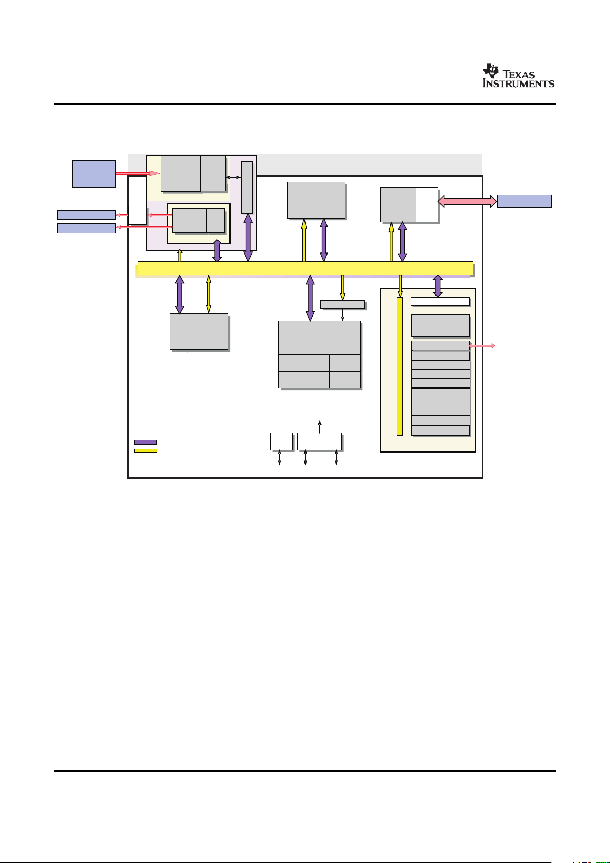
1.3 Functional Block Diagram
Peripherals
64bitDMA/DataBus
JTAG
24MHz 27MHz
(optional)
CCD/
CMOS
Module
DDR2/MDDR16
CLOCK
PLL
CLOCKctrl
PLLs
JTA
JTAG
I/F
Clocks
ARM
z )
ARM926EJ-S_Z8
I-
cach
e
16 K
B
l-cache
16KB
B
RA
M
32 K
B
RAM
32KB
B
D-
cach
e
8K
D-cache
8KB
RO
M
8 K
ROM
8KB
CCD
C
CCDC
3A
3A
DMA / Dataandconfigurationbus
DMA/Dataandconfigurationbus
DDR
MH
z )
DDR
controller
DL
DLL/
PHY
16bit
32bitConfigurationBus
IPIP
E
IPIPE
VPBE
Vide
o
Encod
er
Video
Encoder
10b
DAC
OS
D
OSD
er
c
ARM
ARMINTC
Enhanced
channels
3PCC /TC
(100 MHz
EnhancedDMA
64channels
Compositevideo
DigitalRGB/YUV
Nand /
Nand/SM/
Async/OneNand
(EMIF2.3)
USB 2.0
USB2.0PHY
Speaker
microphone
LD /
ASP (2x)
LD/CM
B
ufferLogic
VPSS
MMC/SD(x2)
SPII/F(x3)
UART (x3)
I2C
Timer/
WDT (x4-64)
GIO
PWM(x4)
RTO
VPFE
Enhanced
channels
3PCC /TC
(100 MHz
MPEG/JPEG
Co-processor
TMS320DM355
Digital Media System-on-Chip (DMSoC)
SPRS463 – SEPTEMBER 2007
Figure 1-1 shows the functional block diagram of the DM355 device.
Figure 1-1. Functional Block Diagram
TMS320DM355 Digital Media System-on-Chip (DMSoC)4 Submit Documentation Feedback
Page 5

www.ti.com
Contents
TMS320DM355
Digital Media System-on-Chip (DMSoC)
SPRS463 – SEPTEMBER 2007
4.1 Absolute Maximum Ratings Over Operating Case
1 TMS320DM355 Digital Media System-on-Chip
Temperature Range
(DMSoC) ................................................... 1
(Unless Otherwise Noted) .......................... 90
1.1 Features .............................................. 1
4.2 Recommended Operating Conditions ............... 91
1.2 Description ............................................ 3
4.3 Electrical Characteristics Over Recommended
1.3 Functional Block Diagram ............................ 4
Ranges of Supply Voltage and Operating Case
2 Device Overview ......................................... 6
Temperature (Unless Otherwise Noted) ............ 92
2.1 Device Characteristics ................................ 6
5 Peripheral Information and Electrical
Specifications ........................................... 93
2.2 Memory Map Summary ............................... 7
5.1 Parameter Information Device-Specific Information 93
2.3 Pin Assignments ...................................... 9
5.2 Recommended Clock and Control Signal Transition
2.4 Pin Functions ........................................ 13
Behavior ............................................. 95
2.5 Pin List .............................................. 36
5.3 Power Supplies ...................................... 95
2.6 Device Support ...................................... 55
5.4 Reset ................................................ 97
3 Detailed Device Description .......................... 59
5.5 Oscillators and Clocks ............................... 98
3.1 ARM Subsystem Overview .......................... 59
5.6 General-Purpose Input/Output (GPIO) ............. 103
3.2 ARM926EJ-S RISC CPU ............................ 60
5.7 External Memory Interface (EMIF) ................. 105
3.3 Memory Mapping .................................... 62
5.8 MMC/SD ........................................... 112
3.4 ARM Interrupt Controller (AINTC) ................... 63
5.9 Video Processing Sub-System (VPSS) Overview . 114
3.5 Device Clocking ..................................... 65
5.10 USB 2.0 ............................................ 127
3.6 PLL Controller (PLLC) ............................... 72
5.11 Universal Asynchronous Receiver/Transmitter
3.7 Power and Sleep Controller (PSC) .................. 76
(UART) ............................................. 129
3.8 System Control Module ............................. 76
5.12 Serial Port Interface (SPI) .......................... 131
3.9 Pin Multiplexing ...................................... 77
5.13 Inter-Integrated Circuit (I2C) ....................... 134
3.10 Device Reset ........................................ 78
5.14 Audio Serial Port (ASP) ............................ 137
3.11 Default Device Configurations ....................... 79
5.15 Timer ............................................... 144
3.12 Device Boot Modes ................................. 82
5.16 Pulse Width Modulator (PWM) ..................... 145
3.13 Power Management ................................. 84
5.17 Real Time Out (RTO) .............................. 147
3.14 64-Bit Crossbar Architecture ........................ 86
5.18 IEEE 1149.1 JTAG ................................ 148
3.15 MPEG/JPEG Overview .............................. 89
6 Mechanical Data ....................................... 151
4 Device Operating Conditions ........................ 90
6.1 Thermal Data for ZCE ............................. 151
6.1.1 Packaging Information ............................. 151
Submit Documentation Feedback Contents 5
Page 6
www.ti.com
PRODUCT PREVIEW
2 Device Overview
2.1 Device Characteristics
TMS320DM355
Digital Media System-on-Chip (DMSoC)
SPRS463 – SEPTEMBER 2007
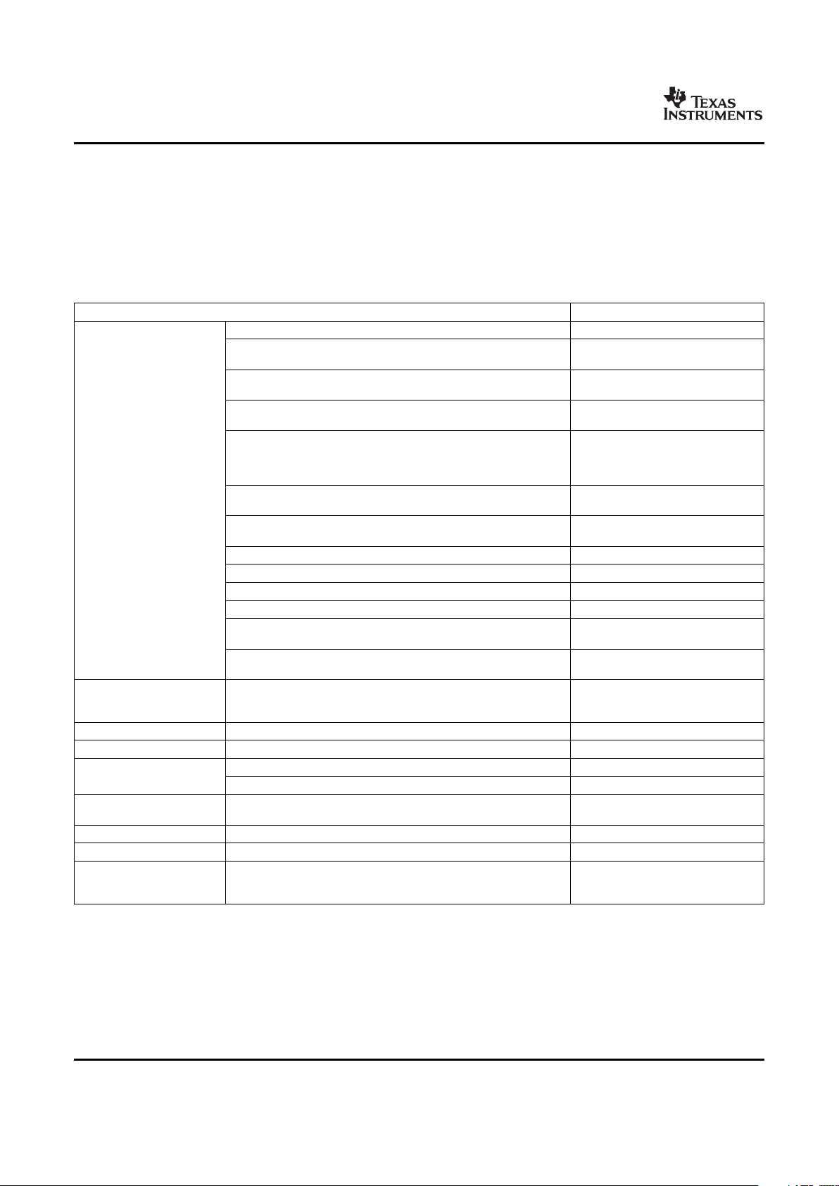
Table 2-1 provides an overview of the DMSoC. The table shows significant features of the device,
including the peripherals, capacity of on-chip RAM, ARM operating frequency, the package type with pin
count, etc.
Table 2-1. Characteristics of the Processor
HARDWARE FEATURES
DDR2 / mDDR Memory Controller DDR2 / mDDR (16-bit bus width)
Asynchronous (8/16-bit bus width)
Asynchronous EMIF (AEMIF)
RAM, Flash (NAND, OneNAND)
Two MMC/SD
Flash Card Interfaces
One SmartMedia/xD
64 independent DMA channels
EDMA
Eight EDMA channels
Three 64-Bit General Purpose (each
configurable as two separate 32-bit
Timers
timers)
Peripherals
One 64-Bit Watch Dog
Not all peripherals pins are
Three (one with RTS and CTS flow
available at the same time
UART
control)
(For more detail, see the
Device Configuration
Three (each supports two slave
SPI
section).
devices)
I2C One (Master/Slave)
Audio Serial Port [ASP] Two ASP
General-Purpose Input/Output Port Up to 104
Pulse width modulator (PWM) Four outputs
One Input (VPFE)
Configurable Video Ports
One Output (VPBE)
High, Full Speed Device
USB 2.0
High, Full, Low Speed Host
ARM
On-Chip CPU Memory Organization 16-KB I-cache, 8-KB D-cache, 32-KB
RAM, 8-KB ROM
JTAG BSDL_ID JTAGID register (address location: 0x01C4 0028) 0x0B73B01F
CPU Frequency (Maximum) MHz ARM 216 MNz and 270 Mhz
Core (V) 1.3 V
Voltage
I/O (V) 3.3 V, 1.8 V
Reference frequency options 24 MHz (typical), 36 MHz
PLL Options
Configurable PLL controller PLL bypass, programmable PLL
BGA Package 13 x 13 mm 337-Pin BGA (ZCE)
Process Technology 90 nm
Product Preview (PP),
Product Status
(1)
Advance Information (AI), PD
or Production Data (PD)
(1) PRODUCTION DATA information is current as of publication date. Products conform to specifications per the terms of the Texas
Instruments standard warranty. Production processing does not necessarily include testing of all parameters.
Device Overview6 Submit Documentation Feedback
Page 7
www.ti.com
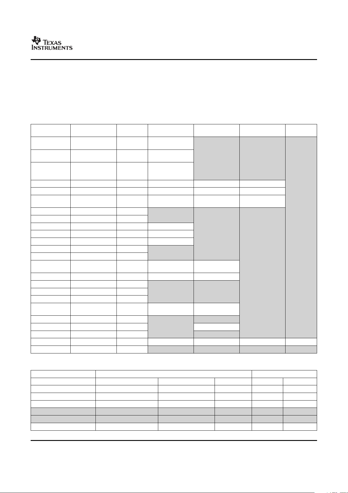
2.2 Memory Map Summary
TMS320DM355
Digital Media System-on-Chip (DMSoC)
SPRS463 – SEPTEMBER 2007
Table 2-3 shows the memory map address ranges of the device. Table 2-3 depicts the expanded map of
the Configuration Space (0x01C0 0000 through 0x01FF FFFF). The device has multiple on-chip memories
associated with its processor and various subsystems. To help simplify software development a unified
memory map is used where possible to maintain a consistent view of device resources across all bus
masters. The bus masters are the ARM, EDMA, USB, and VPSS.
Table 2-2. DM355 Memory Map
Start Address End Address Size (Bytes) ARM EDMA USB VPSS
Mem Map Mem Map Mem Map Mem Map
0x0000 0000 0x0000 3FFF 16K ARM RAM0
(Instruction)
0x0000 4000 0x0000 7FFF 16K ARM RAM1
Reserved Reserved
(Instruction)
0x0000 8000 0x0000 FFFF 32K ARM ROM
(Instruction)
- only 8K used
0x0001 0000 0x0001 3FFF 16K ARM RAM0 (Data) ARM RAM0 ARM RAM0
0x0001 4000 0x0001 7FFF 16K ARM RAM1 (Data) ARM RAM1 ARM RAM1
0x0001 8000 0x0001 FFFF 32K ARM ROM (Data) ARM ROM ARM ROM
- only 8K used
0x0002 0000 0x000F FFFF 896K Reserved
0x0010 0000 0x01BB FFFF 26M
0x01BC 0000 0x01BC 0FFF 4K ARM ETB Mem
0x01BC 1000 0x01BC 17FF 2K ARM ETB Reg Reserved
0x01BC 1800 0x01BC 18FF 256 ARM IceCrusher Reserved
0x01BC 1900 0x01BC FFFF 59136 Reserved
0x01BD 0000 0x01BF FFFF 192K
0x01C0 0000 0x01FF FFFF 4M CFG Bus CFG Bus
Reserved
Peripherals Peripherals
0x0200 0000 0x09FF FFFF 128M ASYNC EMIF (Data) ASYNC EMIF (Data)
0x0A00 0000 0x11EF FFFF 127M - 16K
0x11F0 0000 0x11F1 FFFF 128K Reserved Reserved
0x11F2 0000 0x1FFF FFFF 141M-64K
0x2000 0000 0x2000 7FFF 32K DDR EMIF Control DDR EMIF Control
Regs Regs
0x2000 8000 0x41FF FFFF 544M-32K Reserved
0x4200 0000 0x49FF FFFF 128M Reserved AEMIF - shadow
0x4A00 0000 0x7FFF FFFF 864M Reserved
0x8000 0000 0x8FFF FFFF 256M DDR EMIF DDR EMIF DDR EMIF DDR EMIF
0x9000 0000 0xFFFF FFFF 1792M Reserved Reserved Reserved Reserved
Table 2-3. DM355 ARM Configuration Bus Access to Peripherals
Address Accessibility
Region Start End Size ARM EDMA
EDMA CC 0x01C0 0000 0x01C0 FFFF 64K √ √
EDMA TC0 0x01C1 0000 0x01C1 03FF 1K √ √
EDMA TC1 0x01C1 0400 0x01C1 07FF 1K √ √
Reserved 0x01C1 8800 0x01C1 9FFF 6K √ √
Reserved 0x01C1 A000 0x01C1 FFFF 24K √ √
UART0 0x01C2 0000 0x01C2 03FF 1K √ √
Submit Documentation Feedback Device Overview 7
Page 8
www.ti.com
PRODUCT PREVIEW
TMS320DM355
Digital Media System-on-Chip (DMSoC)
SPRS463 – SEPTEMBER 2007
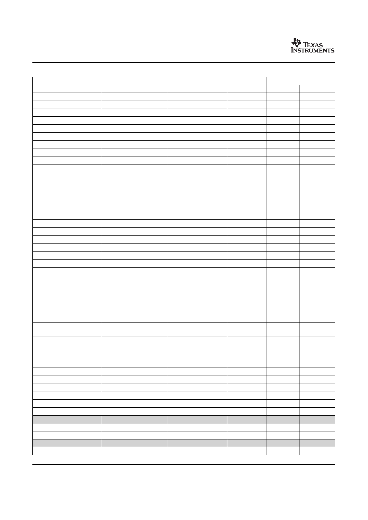
Table 2-3. DM355 ARM Configuration Bus Access to Peripherals (continued)
Address Accessibility
UART1 0x01C2 0400 0x01C2 07FF 1K √ √
Timer4/5 0x01C2 0800 0x01C2 0BFF 1K √ √
Real-time out 0x01C2 0C00 0x01C2 0FFF 1K √ √
I2C 0x01C2 1000 0x01C2 13FF 1K √ √
Timer0/1 0x01C2 1400 0x01C2 17FF 1K √ √
Timer2/3 0x01C2 1800 0x01C2 1BFF 1K √ √
WatchDog Timer 0x01C2 1C00 0x01C2 1FFF 1K √ √
PWM0 0x01C2 2000 0x01C2 23FF 1K √ √
PWM1 0x01C2 2400 0x01C2 27FF 1K √ √
PWM2 0x01C2 2800 0x01C2 2BFF 1K √ √
PWM3 0x01C2 2C00 0x01C2 2FFF 1K √ √
System Module 0x01C4 0000 0x01C4 07FF 2K √ √
PLL Controller 0 0x01C4 0800 0x01C4 0BFF 1K √ √
PLL Controller 1 0x01C4 0C00 0x01C4 0FFF 1K √ √
Power/Sleep Controller 0x01C4 1000 0x01C4 1FFF 4K √ √
ARM Interrupt Controller 0x01C4 8000 0x01C4 83FF 1K √ √
USB OTG 2.0 Regs / RAM 0x01C6 4000 0x01C6 5FFF 8K √ √
SPI0 0x01C6 6000 0x01C6 67FF 2K √ √
SPI1 0x01C6 6800 0x01C6 6FFF 2K √ √
GPIO 0x01C6 7000 0x01C6 77FF 2K √ √
SPI2 0x01C6 7800 0x01C6 FFFF 2K √ √
VPSS Subsystem 0x01C7 0000 0x01C7 FFFF 64K √ √
VPSS Clock Control 0x01C7 0000 0x01C7 007F 128 √ √
Hardware 3A 0x01C7 0080 0x01C7 00FF 128 √ √
Image Pipe (IPIPE) Interface 0x01C7 0100 0x01C7 01FF 256 √ √
On Screen Display 0x01C7 0200 0x01C7 02FF 256 √ √
High Speed Serial IF 0x01C7 0300 0x01C7 03FF 256 √ √
Video Encoder 0x01C7 0400 0x01C7 05FF 512 √ √
CCD Controller 0x01C7 0600 0x01C7 07FF 256 √ √
VPSS Buffer Logic 0x01C7 0800 0x01C7 08FF 256 √ √
CFA Multiply Mask / Lens 0x01C7 0900 0x01C7 09FF 256 √ √
Distortion
Image Pipe (IPIPE) 0x01C7 1000 0x01C7 3FFF 12K √ √
Reserved 0x01CC 0000 0x01CD FFFF 128K √ √
Reserved 0x01CD 0000 0x01CD 007F 128 √ √
Reserved 0x01CD 0380 0x01CD 03FF 128 √ √
Reserved 0x01CD F400 0x01CD F4FF 256 √ √
Sequencer 0x01CD FF00 0x01CD FFFF 256 √ √
Multimedia / SD 1 0x01E0 0000 0x01E0 1FFF 8K √ √
ASP0 0x01E0 2000 0x01E0 3FFF 8K √ √
ASP1 0x01E0 4000 0x01E0 5FFF 8K √ √
UART2 0x01E0 6000 0x01E0 63FF 1K √ √
Reserved 0x01E0 6400 0x01E0 FFFF 39K √ √
ASYNC EMIF Control 0x01E1 0000 0x01E1 0FFF 4K √ √
Multimedia / SD 0 0x01E1 1000 0x01E1 FFFF 60K √ √
Reserved 0x01E2 0000 0x01FF FFFF 1792K √ √
ASYNC EMIF Data (CE0) 0x0200 0000 0x03FF FFFF 32M √ √
Device Overview8 Submit Documentation Feedback
Page 9
www.ti.com
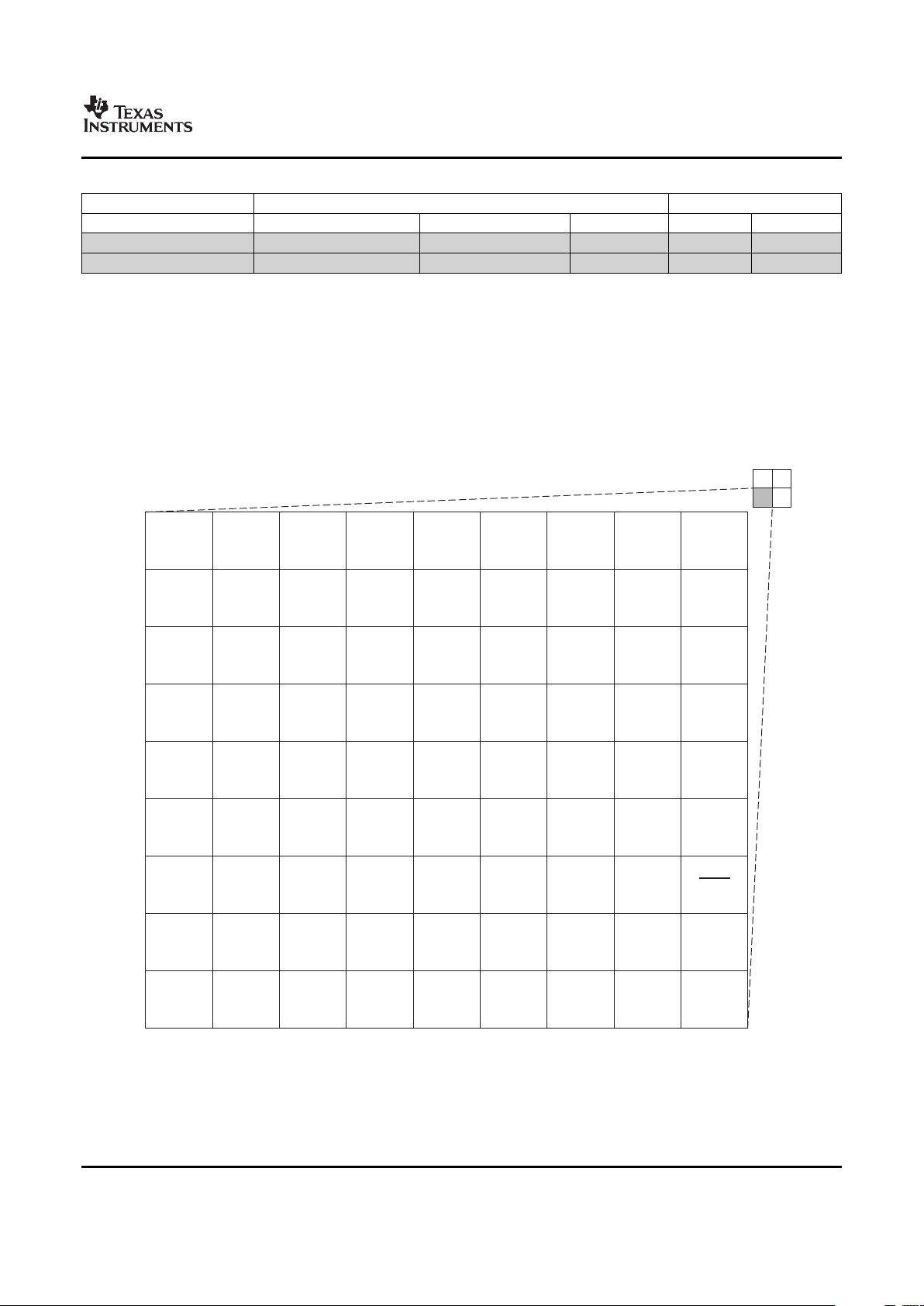
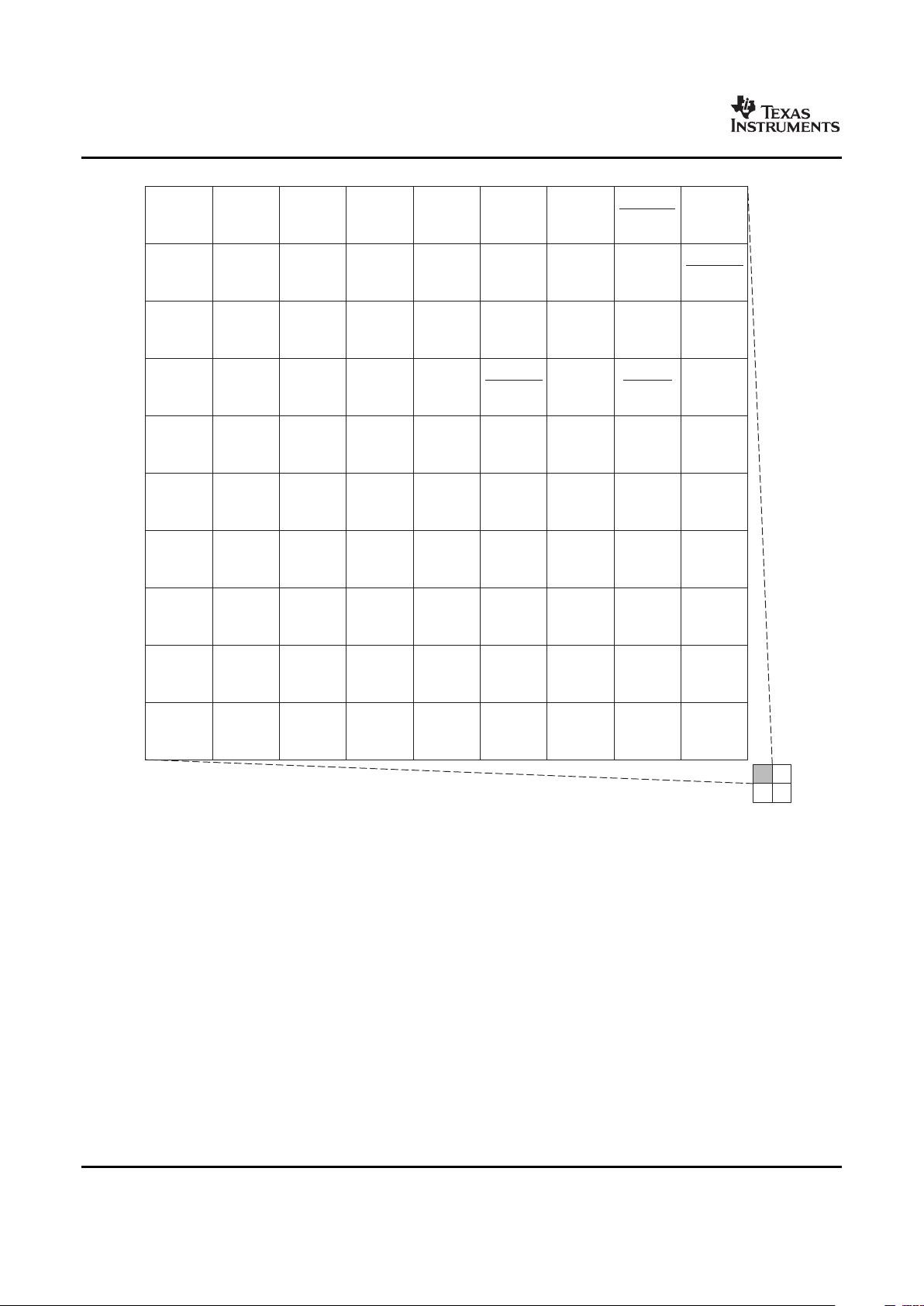
2.3 Pin Assignments
2.3.1 Pin Map (Bottom View)
9
J
8
VSSA_
PLL2
7
VDDA3P3
USB
6
5
4
31
H
G
VDDA1P2
_USB
V
SS
F
E
D
CIN2
C
B
A
VREF
CIN3CIN0DP
VDDA_
PLL2
V
SS
VVALIDFIELDVCLK
V
SS
V
SS
VDDSHV
V
DD
VSYNCEXTCLKVFB
VDDSHVVDDSHV4VDDSHV4VDDSHV4HSYNCCOUT0COUT1TVOUT
TDOEMU0EMU1
VSS_USB
USB_
VBUS
COUT2COUT3IOUT
TDITMS
VSS_USB
USB_IDCOUT4
V
SS
TRSTVSSREFUSB_R1
VDDD1P2
USB
USB_DRV
VBUS
V
DD
YOUT7COUT5
MXO1
V
SS
VSS_USBVDDA_
USB_PLL
V
SS
YOUT5YOUT4YOUT0
MXI1
V
SS
USB_DPUSB_DM
V
SS
YOUT6YOUT2
V
DD
V
DD
2
V
SS
V
SS
V
SS
IBIAS
V
SS
COUT6
COUT7
YOUT3
YOUT1
TMS320DM355
Digital Media System-on-Chip (DMSoC)
SPRS463 – SEPTEMBER 2007
Table 2-3. DM355 ARM Configuration Bus Access to Peripherals (continued)
Address Accessibility
ASYNC EMIF Data (CE1) 0x0400 0000 0x05FF FFFF 32M √ √
Reserved 0x0A00 0000 0x0BFF FFFF 32M √ √
Reserved 0x0C00 0000 0x0FFF FFFF 64M √ √
Extensive use of pin multiplexing is used to accommodate the largest number of peripheral functions in
the smallest possible package. Pin multiplexing is controlled using a combination of hardware
configuration at device reset and software programmable register settings.
Figure 2-1 through Figure 2-4 show the pin assignments in four quadrants (A, B, C, and D). Note that
micro-vias are not required. Contact your TI representative for routing recommendations.
Figure 2-1. Pin Map [Quadrant A]
Submit Documentation Feedback Device Overview 9
Page 10
www.ti.com
PRODUCT PREVIEW
W
9
DDR_CLK
8
DDR_CLK
7654
DDR_A5
32
DDR_A2
1
V
DDR_A7DDR_A4DDR_A0
U
V
SS
T
PCLK
R
P
N
M
L
K
DDR_A11DDR_A9DDR_A8
V
SS
DDR_CASDDR_
BA[2]
DDR_A12DDR_A10DDR_A1
V
SS
DDR_
BA[0]
DDR_
BA[1]
DDR_A13DDR_A6
DDR_A3
V
SS
V
SS
V
SS
V
SS
DDR_ZNDDR_CSDDR_RAS
V
SS
V
SS
MXO2
V
DDS
V
DD
V
DD
V
SS
CAM_WEN_
FIELD
CAM_VDYIN3
V
SS
MXI2
V
DDS
VDDSHV3VDDSHV3VDDSHV3
YIN0YIN2YIN4YIN1MX2GND
V
SS
V
SS
V
DD
CAM_HDCIN7LVIREF
V
SS
V
DDS
V
SS
V
SS
V
SS
YIN5YIN6CIN5
VDDA18V
_CCP2
SN
V
SS
VSS_DACVDDA18V
_DAC
VDDSHV1
YIN7CIN4CIN1
V
SS
SP
V
SS
VDDSHV2
V
DD
CIN6
V
SS
VSSA_
CCP2
DN
TMS320DM355
Digital Media System-on-Chip (DMSoC)
SPRS463 – SEPTEMBER 2007
Figure 2-2. Pin Map [Quadrant B]
Device Overview10 Submit Documentation Feedback
Page 11

www.ti.com
V
DD
19
W
18
DDR_
GATE0
17
DDR_
DQ15
16
DDR_
DQ13
15
DDR_
DQ11
14
DDR_
DQ10
13
DDR_DQ7
12
DDR_DQ5
11
DDR_DQ1
10
DDR_WE
EM_A13
V
V
SS
DDR_
GATE1
DDR_
DQ14
DDR_
DQS[1]
DDR_DQ9DDR_DQ6
DDR_
DQS[0]
DDR_DQ0DDR_CKE
EM_A12
U
UART0_
RXD
V
SS
DDR_
DQ12
DDR_
DQM[1]
V
SS
DDR_DQ8DDR_DQ4DDR_DQ2DDR_
VREF
EM_A8
T
UART0_
TXD
V
DD
V
SS
V
DDS
DDR_
DQM[0]
DDR_DQ3
EM_A5
R
EM_A10
UART1_
TXD
EM_A11
UART1_
RXD
I2C_SCLI2C_SDA
V
DDS
DDR_
VSSDLL
DDR_
VDDDLL
EM_BA1
P
EM_A6
EM_A9EM_A7EM_A4
V
DDS
V
DDS
V
DDS
V
DDS
V
DDS
EM_BA0
N
EM_A3EM_A1EM_A2
V
SS
VDDSHVVDDSHV
EM_D14
M
EM_D15
V
SS
EM_A0EM_D13
V
SS
VDDSHVVDDSHVVDDSHVVDDSHV
EM_D10
L
EM_D12EM_D11EM_D8EM_D4
V
SS
V
SS
VDDSHV
V
DD
V
DD
V
DD
V
DD
V
SS
V
SS
EM_D7
K
EM_D9EM_D6VDDSHV
TMS320DM355
Digital Media System-on-Chip (DMSoC)
SPRS463 – SEPTEMBER 2007
Figure 2-3. Pin Map [Quadrant C]
Submit Documentation Feedback Device Overview 11
Page 12

www.ti.com
PRODUCT PREVIEW
19181716151413121110
EM_D5
J
EM_D2
H
EM_CE1
G
F
E
D
C
VDDSHV
B
A
EM_D3EM_D1EM_CE0EM_WE
V
SS
V
DD
V
DD
V
DD
V
SS
EM_D0
V
DD
EM_ADV
ASP0_
DX
V
SS
V
DD
VSS_PLL
1
V
SS
V
DD
EM_WAIT
ASP0_
FSX
GIO3
VDDA_
PLL1
V
DD
EM_OE
ASP0_
CLKX
ASP0_
CLKR
ASP0_
FSR
GIO2VDDSHVVDDSHVVDDSHVVDDSHVVDDSHV
EM_CLK
ASP0_
DR
ASP1_
FSR
ASP1_
FSX
V
SS
GIO1
SPI1_
SDENA
SPI1_SDORTCKTCK
ASP1_
CLKX
ASP1_
CLKR
ASP1_
CLKS
GIO5
SD0_
DATA1
CLKOUT1RESET
ASP1_
DR
ASP1_
DX
GIO7GIO0
MMCSD1_
CLK
MMCSD0_
CMD
SPI1_
SCLK
SPI0_
SCLK
CLKOUT3MX1GND
V
DD
V
SS
GIO6
MMCSD1_
DATA0
MMCSD1_
DATA3
MMCSD1_
DATA2
GIO4
MMCSD1_
CMD
MMCSD1_
DATA1
MMCSD0_
CLK
MMCSD0_
DATA0
MMCSD0_
DATA3
MMCSD0_
DATA2
SPI1_SDI
SPI0_
SDENA
SPI0_SDI
SPI0_SDO
CLKOUT2
V
SS
V
DD
TMS320DM355
Digital Media System-on-Chip (DMSoC)
SPRS463 – SEPTEMBER 2007
Figure 2-4. Pin Map [Quadrant D]
12 Device Overview Submit Documentation Feedback
Page 13
www.ti.com
2.4 Pin Functions
2.4.1 Image Data Input - Video Processing Front End
TMS320DM355
Digital Media System-on-Chip (DMSoC)
SPRS463 – SEPTEMBER 2007
The pin functions tables (Table 2-4 through Table 2-22 ) identify the external signal names, the associated
pin (ball) numbers along with the mechanical package designator, the pin type, whether the pin has any
internal pullup or pulldown resistors, and a functional pin description. For more detailed information on
device configuration, peripheral selection, multiplexed/shared pins, and debugging considerations, see
Section 3 . For the list of all pin in chronological order see Section 2.5
The CCD Controller module in the Video Processing Front End has an external signal interface for image
data input. It supports YUV (YC) inputs as well as Bayer RGB and complementary input signals (I.e.,
image data input).
The definition of the CCD controller data input signals depend on the input mode selected.
• In 16-bit YCbCr mode, the Cb and Cr signals are multiplexed on the Cl signals and the order is
configurable (i.e., Cb first or Cr first).
• In 8-bit YCbCr mode, the Y, Cb, and Cr signals are multiplexed and not only is the order selectable,
but also the half of the bus used.
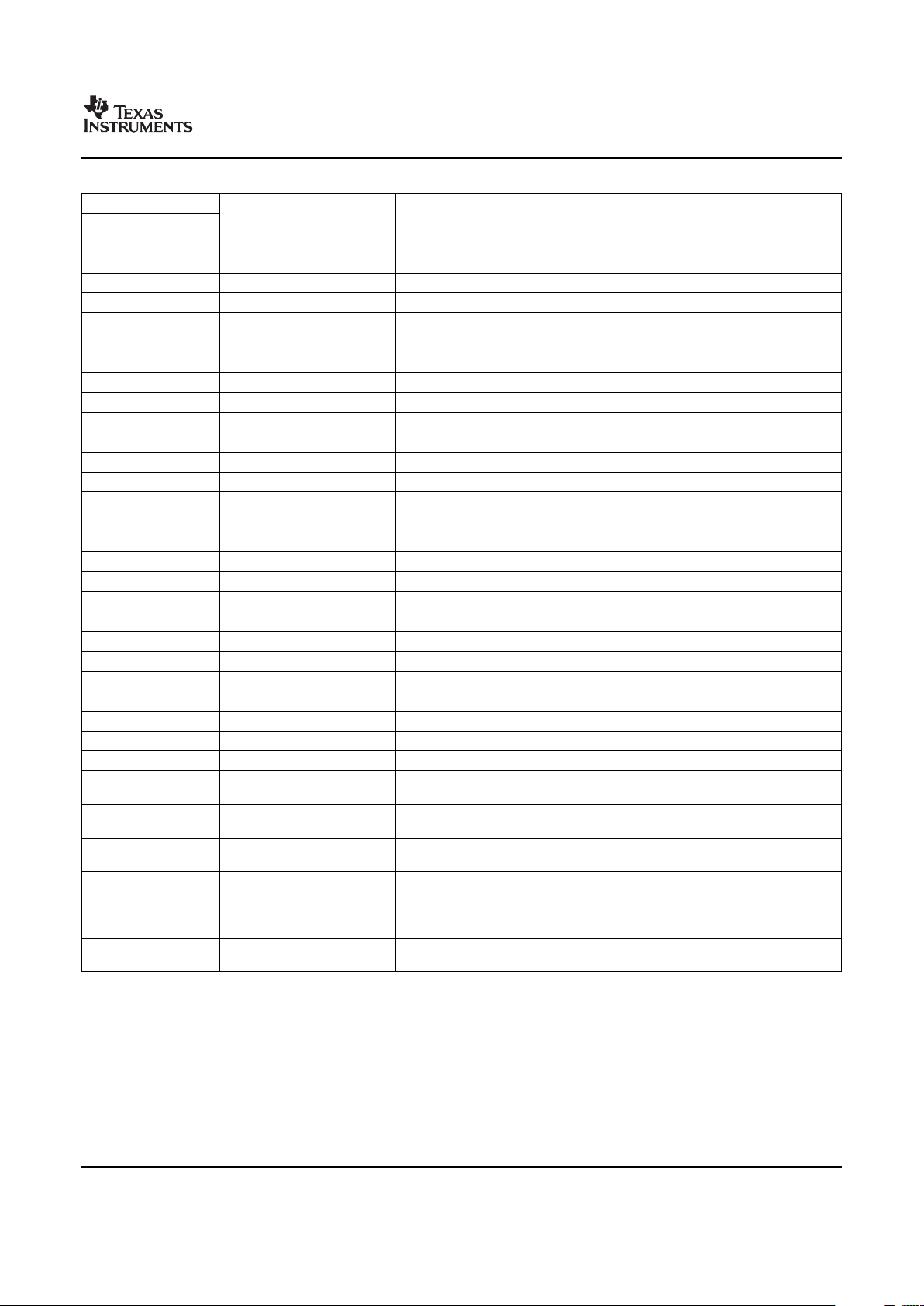
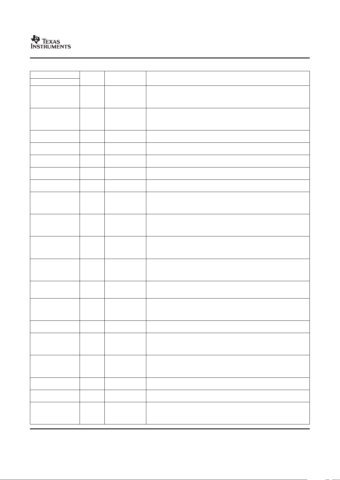
Table 2-4. CCD Controller Signals for Each Input Mode
PIN NAME CCD 16-BIT YCbCr 8-BIT YCbCr
Cl7 Cb7,Cr7 Y7,Cb7,Cr7
Cl6 Cb6,Cr6 Y6,Cb6,Cr6
Cl5 CCD13 Cb5,Cr5 Y5,Cb5,Cr5
Cl4 CCD12 Cb4,Cr4 Y4,Cb4,Cr4
Cl3 CCD11 Cb3,Cr3 Y3,Cb3,Cr3
Cl2 CCD10 Cb2,Cr2 Y2,Cb2,Cr2
Cl1 CCD9 Cb1,Cr1 Y1,Cb1,Cr1
Cl0 CCD8 Cb0,Cr0 Y0,Cb0,Cr0
Yl7 CCD7 Y7 Y7,Cb7,Cr7
Yl6 CCD6 Y6 Y6,Cb6,Cr6
Yl5 CCD5 Y5 Y5,Cb5,Cr5
Yl4 CCD4 Y4 Y4,Cb4,Cr4
Yl3 CCD3 Y3 Y3,Cb3,Cr3
Yl2 CCD2 Y2 Y2,Cb2,Cr2
Yl1 CCD1 Y1 Y1,Cb1,Cr1
Yl0 CCD0 Y0 Y0,Cb0,Cr0
Submit Documentation Feedback Device Overview 13
Page 14

www.ti.com
PRODUCT PREVIEW
TMS320DM355
Digital Media System-on-Chip (DMSoC)
SPRS463 – SEPTEMBER 2007
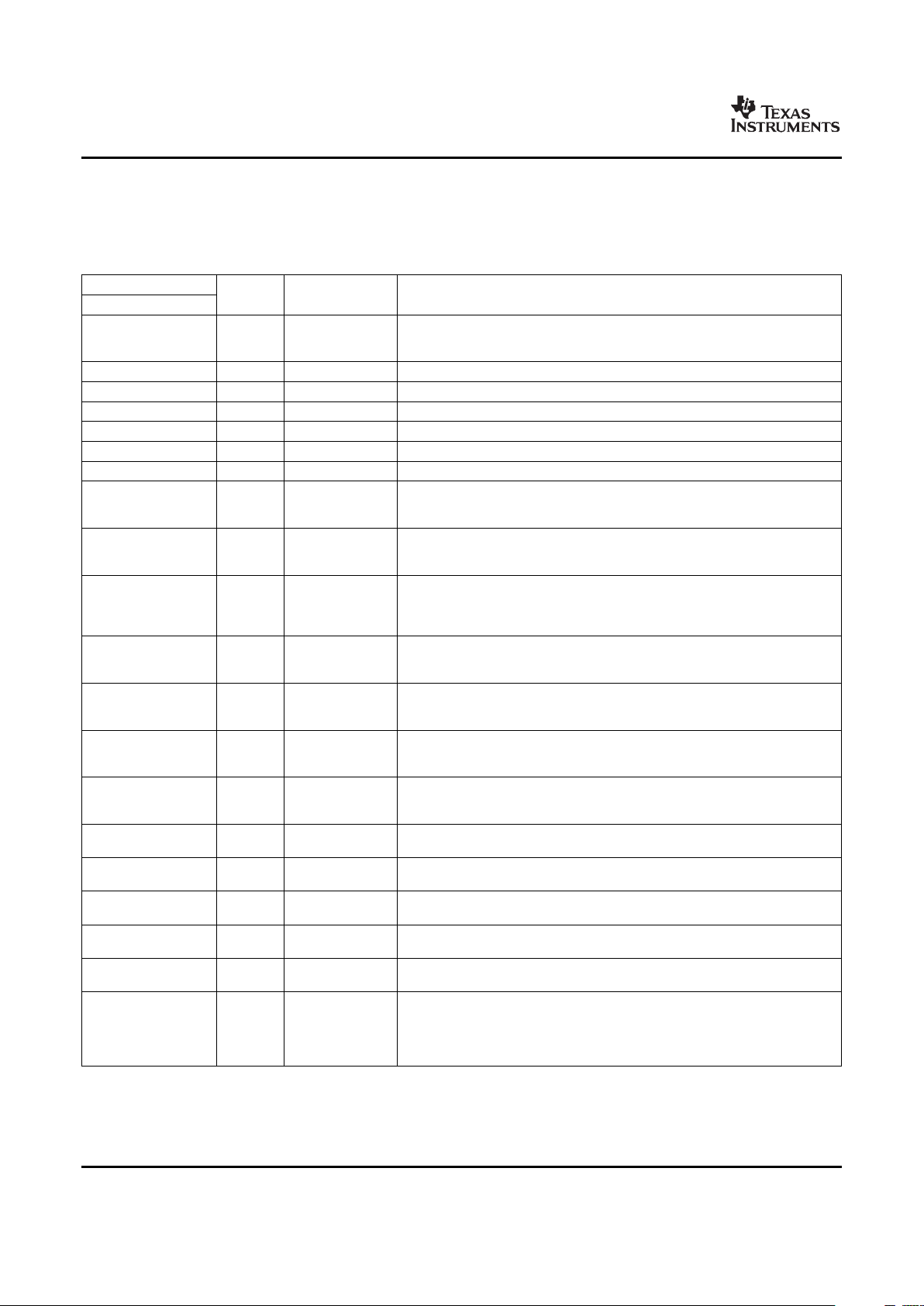
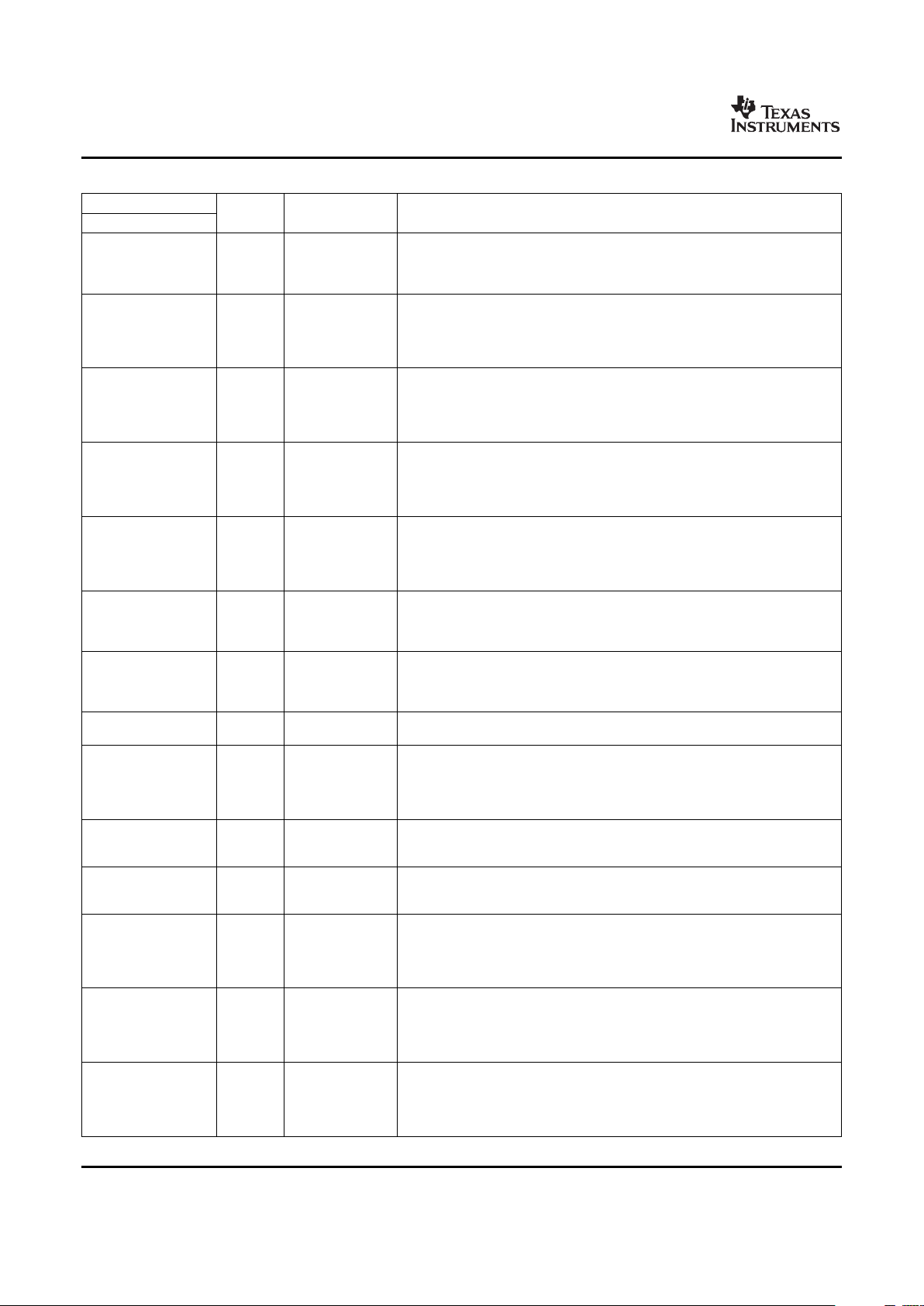
Table 2-5. CCD Controller/Video Input Terminal Functions
TERMINAL
TYPE
(1)
OTHER
(2) (3)
DESCRIPTION
NAME NO.
Standard CCD Analog Front End (AFE): NOT USED
• YCC 16-bit: Time multiplexed between chroma: CB/SR[07]
CIN7/
PD
• YCC 8-bit (which allows for two simultaneous decoder inputs), it is time
GIO101/ N3 I/O/Z
V
DD_VIN
multiplexed between luma and chroma of the upper channel. Y/CB/CR[07]
SPI2_SCLK
SPI: SPI2 Clock
GIO: GIO[101]
Standard CCD Analog Front End (AFE): NOT USED
• YCC 16-bit: Time multiplexed between chroma: CB/SR[06]
CIN6/
PD
• YCC 8-bit (which allows for two simultaneous decoder inputs), it is time
GIO100/ K5 I/O/Z
V
DD_VIN
multiplexed between luma and chroma of the upper channel. Y/CB/CR[06]
SPI2_SDO
SPI: SPI2 Data Out
GIO: GIO[100]
Standard CCD Analog Front End (AFE): Raw[13]
CIN5/ • YCC 16-bit: Time multiplexed between chroma: CB/SR[05]
GIO099/ PD
• YCC 8-bit (which allows for two simultaneous decoder inputs), it is time
M3 I/O/Z
SPI2_SDEN V
DD_VIN
multiplexed between luma and chroma of the upper channel. Y/CB/CR[05]
A[0]
SPI: SPI2 Chip Select
GIO: GIO[099]
Standard CCD Analog Front End (AFE): Raw[12]
CIN4/ • YCC 16-bit: Time multiplexed between chroma: CB/SR[04]
GIO098/ PD
• YCC 8-bit (which allows for two simultaneous decoder inputs), it is time
L4 I/O/Z
SPI2_SDEN V
DD_VIN
multiplexed between luma and chroma of the upper channel. Y/CB/CR[04]
A[1]
SPI: SPI2 Data In
GIO: GIO[098]
Standard CCD Analog Front End (AFE): Raw[11]
• YCC 16-bit: Time multiplexed between chroma: CB/SR[03]
CIN3/ PD
J4 I/O/Z
• YCC 8-bit (which allows for two simultaneous decoder inputs), it is time
GIO097/ V
DD_VIN
multiplexed between luma and chroma of the upper channel. Y/CB/CR[03]
GIO: GIO[097]
Standard CCD Analog Front End (AFE): Raw[10]
• YCC 16-bit: Time multiplexed between chroma: CB/SR[02]
CIN2/ PD
J5 I/O/Z
• YCC 8-bit (which allows for two simultaneous decoder inputs), it is time
GIO096/ V
DD_VIN
multiplexed between luma and chroma of the upper channel. Y/CB/CR[02]
GIO: GIO[097]
Standard CCD Analog Front End (AFE): Raw[09]
• YCC 16-bit: Time multiplexed between chroma: CB/SR[01]
CIN1/ PD
L3 I/O/Z
• YCC 8-bit (which allows for two simultaneous decoder inputs), it is time
GIO095/ V
DD_VIN
multiplexed between luma and chroma of the upper channel. Y/CB/CR[01]
GIO: GIO[095]
Standard CCD Analog Front End (AFE): Raw[08]
• YCC 16-bit: Time multiplexed between chroma: CB/SR[00]
CIN0/ PD
J3 I/O/Z
• YCC 8-bit (which allows for two simultaneous decoder inputs), it is time
GIO094/ V
DD_VIN
multiplexed between luma and chroma of the upper channel. Y/CB/CR[00]
GIO: GIO[094]
Standard CCD Analog Front End (AFE): Raw[07]
• YCC 16-bit: Time multiplexed between chroma: Y[07]
YIN7/ PD
L5 I/O/Z
• YCC 8-bit (which allows for two simultaneous decoder inputs), it is time
GIO093 V
DD_VIN
multiplexed between luma and chroma of the upper channel. Y/CB/CR[07]
GIO: GIO[093]
Standard CCD Analog Front End (AFE): Raw[06]
• YCC 16-bit: Time multiplexed between chroma: Y[06]
YIN6/ PD
M4 I/O/Z
• YCC 8-bit (which allows for two simultaneous decoder inputs), it is time
GIO092 V
DD_VIN
multiplexed between luma and chroma of the upper channel. Y/CB/CR[06]
GIO: GIO[092]
(1) I = Input, O = Output, Z = High impedance, S = Supply voltage, GND = Ground, A = Analog signal.
(2) PD = internal pull-down, PU = internal pull-up. (To pull up a signal to the opposite supply rail, a 1 k Ω resistor should be used.)
(3) Specifies the operating I/O supply voltage for each signal. See Section 5.3 , Power Supplies for more detail.
Device Overview14 Submit Documentation Feedback
Page 15

www.ti.com
2.4.2 Image Data Output - Video Processing Back End (VPBE)
TMS320DM355
Digital Media System-on-Chip (DMSoC)
SPRS463 – SEPTEMBER 2007
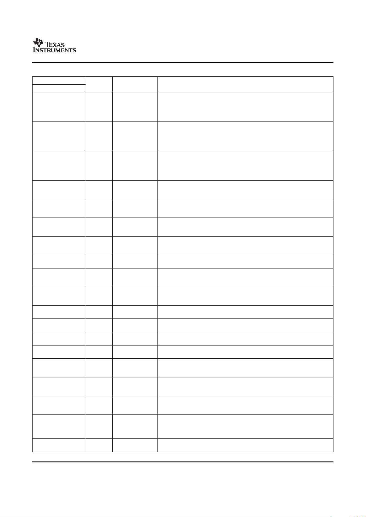
Table 2-5. CCD Controller/Video Input Terminal Functions (continued)
TERMINAL
TYPE
(1)
OTHER
(2) (3)
DESCRIPTION
NAME NO.
Standard CCD Analog Front End (AFE): Raw[05]
• YCC 16-bit: Time multiplexed between chroma: Y[05]
YIN5/ PD
M5 I/O/Z
• YCC 8-bit (which allows for two simultaneous decoder inputs), it is time
GIO091 V
DD_VIN
multiplexed between luma and chroma of the upper channel. Y/CB/CR[05]
GIO: GIO[091]
Standard CCD Analog Front End (AFE): Raw[04]
• YCC 16-bit: Time multiplexed between chroma: Y[04]
YIN4/ PD
P3 I/O/Z
• YCC 8-bit (which allows for two simultaneous decoder inputs), it is time
GIO090 V
DD_VIN
multiplexed between luma and chroma of the upper channel. Y/CB/CR[04]
GIO: GIO[090]
Standard CCD Analog Front End (AFE): Raw[03]
• YCC 16-bit: Time multiplexed between chroma: Y[03]
YIN3/ PD
R3 I/O/Z
• YCC 8-bit (which allows for two simultaneous decoder inputs), it is time
GIO089 V
DD_VIN
multiplexed between luma and chroma of the upper channel. Y/CB/CR[03]
GIO: GIO[089]
Standard CCD Analog Front End (AFE): Raw[02]
• YCC 16-bit: Time multiplexed between chroma: Y[02]
YIN2/ PD
P4 I/O/Z
• YCC 8-bit (which allows for two simultaneous decoder inputs), it is time
GIO088 V
DD_VIN
multiplexed between luma and chroma of the upper channel. Y/CB/CR[02]
GIO: GIO[088]
Standard CCD Analog Front End (AFE): Raw[01]
• YCC 16-bit: Time multiplexed between chroma: Y[01]
YIN1/ PD
P2 I/O/Z
• YCC 8-bit (which allows for two simultaneous decoder inputs), it is time
GIO087 V
DD_VIN
multiplexed between luma and chroma of the upper channel. Y/CB/CR[01]
GIO: GIO[087]
Standard CCD Analog Front End (AFE): Raw[00]
• YCC 16-bit: Time multiplexed between chroma: Y[00]
YIN0/ PD
P5 I/O/Z
• YCC 8-bit (which allows for two simultaneous decoder inputs), it is time
GIO086 V
DD_VIN
multiplexed between luma and chroma of the upper channel. Y/CB/CR[00]
GIO: GIO[086]
Horizontal synchronization signal that can be either an input (slave mode) or an
CAM_HD/ PD
N5 I/O/Z output (master mode). Tells the CCDC when a new line starts.
GIO085 V
DD_VIN
GIO: GIO[085]
Vertical synchronization signal that can be either an input (slave mode) or an output
CAM_VD PD
R4 I/O/Z (master mode). Tells the CCDC when a new frame starts.
GIO084 V
DD_VIN
GIO: GIO[084]
Write enable input signal is used by external device (AFE/TG) to gate the DDR
output of the CCDC module. Alternately, the field identification input signal is used
CAM_WEN
PD by external device (AFE/TG) to indicate which of two frames is input to the CCDC
_FIELD\ R5 I/O/Z
V
DD_VIN
module for sensors with interlaced output. CCDC handles 1- or 2-field sensors in
GIO083
hardware.
GIO: GIO[083]
PCLK/ PD Pixel clock input (strobe for lines C17 through Y10)
T3 I/O/Z
GIO082 V
DD_VIN
GIO: GIO[0082]
The Video Encoder/Digital LCD interface module in the video processing back end has an external signal
interface for digital image data output as described in Table 2-7 and Table 2-8 .
The digital image data output signals support multiple functions / interfaces, depending on the display
mode selected. The following table describes these modes. Parallel RGB mode with more than RGB565
signals requires enabling pin multiplexing to support (i.e., for RGB666 mode).
Submit Documentation Feedback Device Overview 15
Page 16
www.ti.com
PRODUCT PREVIEW
TMS320DM355
Digital Media System-on-Chip (DMSoC)
SPRS463 – SEPTEMBER 2007
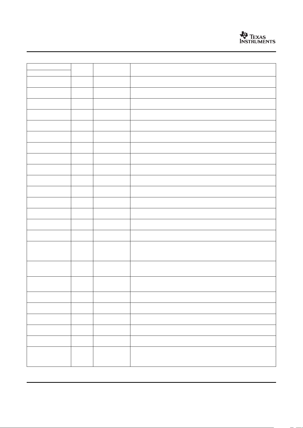
Table 2-6. Signals for VPBE Display Modes
PIN NAME YCC16 YCC8/ PRGB SRGB
REC656
HSYNC HSYNC HSYNC HSYNC HSYNC
GIO073
VSYNC VSYNC VSYNC VSYNC VSYNC
GIO072
LCD_OE As needed As needed As needed As needed
GIO071
FIELD As needed As needed As needed As needed
GIO070
R2
PWM3C
EXTCLK As needed As needed As needed As needed
GIO069
B2
PWM3D
VCLK VCLK VCLK VCLK VCLK
GIO068
YOUT7 Y7 Y7,Cb7,Cr7 R7 Data7
YOUT6 Y6 Y6,Cb6,Cr6 R6 Data6
YOUT5 Y5 Y5,Cb5,Cr5 R5 Data5
YOUT4 Y4 Y4,Cb4,Cr4 R4 Data4
YOUT3 Y3 Y3,Cb3,Cr3 R3 Data3
YOUT2 Y2 Y2,Cb2,Cr2 G7 Data2
YOUT1 Y1 Y1,Cb1,Cr1 G6 Data1
YOUT0 Y0 Y0,Cb0,Cr0 G5 Data0
COUT7 C7 LCD_AC G4 LCD_AC
GIO081
PWM0
COUT6 C6 LCD_OE G3 LCD_OE
GIO080
PWM1
COUT5 C5 BRIGHT G2 BRIGHT
GIO079
PWM2A
RTO0
COUT4 C4 PWM B7 PWM
GIO078
PWM2B
RTO1
COUT3 C3 CSYNC B6 CSYNC
GIO077
PWM2C
RTO2
COUT2 C2 - B5 GIO076
PWM2D
RTO3
COUT1 C1 - B4 GIO075
PWM3A
COUT0 C0 - B3 GIO074
PWM3B
Device Overview16 Submit Documentation Feedback
Page 17
www.ti.com
TMS320DM355
Digital Media System-on-Chip (DMSoC)
SPRS463 – SEPTEMBER 2007
Table 2-7. Digital Video Terminal Functions
TERMINAL
TYPE
(1)
OTHER
(2) (3)
DESCRIPTION
(4)
NAME NO.
YOUT7-R7 C2 I/O/Z V
DD_VOUT
Digital Video Out: VENC settings determine function
YOUT6-R6 A4 I/O/Z V
DD_VOUT
Digital Video Out: VENC settings determine function
YOUT5-R5 B4 I/O/Z V
DD_VOUT
Digital Video Out: VENC settings determine function
YOUT4-R4 B3 I/O/Z V
DD_VOUT
Digital Video Out: VENC settings determine function
YOUT3-R3 B2 I/O/Z V
DD_VOUT
Digital Video Out: VENC settings determine function
YOUT2-G7 A3 I/O/Z V
DD_VOUT
Digital Video Out: VENC settings determine function
YOUT1-G6 A2 I/O/Z V
DD_VOUT
Digital Video Out: VENC settings determine function
YOUT0-G5 B1 I/O/Z V
DD_VOUT
Digital Video Out: VENC settings determine function
COUT7G4/GIO081 C2 I/O/Z V
DD_VOUT
Digital Video Out: VENC settings determine function GIO: GIO[081] PWM0
/PWM0
COUT6-G3
/GIO080 D2 I/O/Z V
DD_VOUT
Digital Video Out: VENC settings determine function GIO: GIO[080] PWM1
/PWM1
COUT5-G2
/ GIO079 /
C1 I/O/Z V
DD_VOUT
Digital Video Out: VENC settings determine function GIO: GIO[079] PWM2A RTO0
PWM2A /
RTO0
COUT4-B7 /
GIO078 /
D3 I/O/Z V
DD_VOUT
Digital Video Out: VENC settings determine function GIO: GIO[078] PWM2B RTO1
PWM2B /
RTO1
COUT3-B6 /
GIO077 /
E3 I/O/Z V
DD_VOUT
Digital Video Out: VENC settings determine function GIO: GIO[077] PWM2C RTO2
PWM2C /
RTO2
COUT2-B5 /
GIO076 /
E4 I/O/Z V
DD_VOUT
Digital Video Out: VENC settings determine function GIO: GIO[076] PWM2D RTO3
PWM2D /
RTO3
COUT1-B4 / Digital Video Out: VENC settings determine function
GIO075 / F3 I/O/Z V
DD_VOUT
GIO: GIO[075]
PWM3A PWM3A
COUT0-B3 / Digital Video Out: VENC settings determine function
GIO074 / F4 I/O/Z V
DD_VOUT
GIO: GIO[074]
PWM3B PWM3B
HSYNC / PD Video Encoder: Horizontal Sync
F5 I/O/Z
GIO073 V
DD_VOUT
GIO: GIO[073]
VSYNC / PD Video Encoder: Vertical Sync
G5 I/O/Z
GIO072 V
DD_VOUT
GIO: GIO[072]
FIELD / Video Encoder: Field identifier for interlaced display formats
GIO070 / GIO: GIO[070]
H4 I/O/Z V
DD_VOUT
R2 / Digital Video Out: R2
PWM3C PWM3C
Video Encoder: External clock input, used if clock rates > 27 MHz are needed, e.g.
EXTCLK /
74.25 MHz for HDTV digital output
GIO069 / PD
G3 I/O/Z GIO: GIO[069]
B2 / V
DD_VOUT
Digital Video Out: B2
PWM3D
PWM3D
VCLK / Video Encoder: Video Output Clock
H3 I/O/Z V
DD_VOUT
GIO068 GIO: GIO[068]
(1) I = Input, O = Output, Z = High impedance, S = Supply voltage, GND = Ground, A = Analog signal.
(2) Specifies the operating I/O supply voltage for each signal. See Section 5.3 , Power Supplies for more detail.
(3) PD = pull-down, PU = pull-up. (To pull up a signal to the opposite supply rail, a 1 k Ω resistor should be used.)
(4) To reduce EMI and reflections, depending on the trace length, approximately 22 Ω to 50 Ω damping resistors are recommend on the
following outputs placed near the DM355: YOUT(0-7),COUT(0-7), HSYNC,VSYNC,LCD_OE,FIELD,EXTCLK,VCLK. The trace lengths
should be minimized.
Submit Documentation Feedback Device Overview 17
Page 18
www.ti.com
PRODUCT PREVIEW
2.4.3 Asynchronous External Memory Interface (AEMIF)
TMS320DM355
Digital Media System-on-Chip (DMSoC)
SPRS463 – SEPTEMBER 2007
Table 2-8. Analog Video Terminal Functions
TERMINAL
TYPE
(1)
OTHER
(2)
DESCRIPTION
NAME NO.
Video DAC: Reference voltage output (0.45V, 0.1uF to GND). When the DAC is not
VREF J7 A I/O/Z
used, the VREF signal should be connected to VSS.
Video DAC: Pre video buffer DAC output (1000 ohm to VFB). When the DAC is not
IOUT E1 A I/O/Z
used, the IOUT signal should be connected to VSS.
Video DAC: External resistor (2550 Ohms to GND) connection for current bias
IBIAS F2 A I/O/Z configuration. When the DAC is not used, the IBIAS signal should be connected to
VSS.
Video DAC: Pre video buffer DAC output (1000 Ohms to IOUT, 1070 Ohms to
VFB G1 A I/O/Z
TVOUT). When the DAC is not used, the VFB signal should be connected to VSS.
Video DAC: Analog Composite NTSC/PAL output (SeeFigure 5-31 andFigure 5-32 for
TVOUT F1 A I/O/Z V circuit connection). When the DAC is not used, the TVOUT signal should be left as a
No Connect or connected to VSS.
Video DAC: Analog 1.8V power. When the DAC is not used, the V
DDA18_DAC
signal
V
DDA18_DAC
L7 PWR
should be connected to VSS.
Video DAC: Analog 1.8V ground. When the DAC is not used, the V
SSA_DAC
signal
V
SSA_DAC
L8 GND
should be connected to VSS.
(1) I = Input, O = Output, Z = High impedance, S = Supply voltage, GND = Ground, A = Analog signal. Specifies the operating I/O supply
voltage for each signal. See Section 5.3 , Power Supplies for more detail.
(2) PD = pull-down, PU = pull-up. (To pull up a signal to the opposite supply rail, a 1 k Ω resistor should be used.)
The Asynchronous External Memory Interface (AEMIF) signals support AEMIF, NAND, and OneNAND.
Table 2-9. Asynchronous EMIF/NAND/OneNAND Terminal Functions
TERMINAL
TYPE
(1)
OTHER
(2) (3)
DESCRIPTION
NAME NO.
Async EMIF: Address bus bit[13]
EM_A13/
PD GIO: GIO[67]
GIO067/ V19 I/O/Z
V
DD
System: BTSEL[1:0] sampled at power-on-reset to determine boot method. Used
BTSEL[1]
to drive boot status LED signal (active low) in ROM boot modes.
EM_A12/ Async EMIF: Address bus bit[12]
PD
GIO066/ U19 I/O/Z GIO: GIO[66]
V
DD
BTSEL[0] System: BTSEL[1:0] sampled at power-on-reset to determine boot method.
Async EMIF: Address bus bit[11]
EM_A11/
PU GIO: GIO[65]
GIO065/ R16 I/O/Z
V
DD
AECFG[3:0] sampled at power-on-reset to AECFG configuration. AECFG[3] sets
AECFG[3]
default for PinMux2_EM_D15_8: AEMIF default bus width (16 or 8 bits)
Async EMIF: Address bus bit[10]
EM_A10/ GIO: GIO[64]
PU
GIO064/ R18 I/O/Z AECFG[3:0] sampled at power-on-reset to AECFG configuration. AECFG[2:1]
V
DD
AECFG[2] sets default for PinMux2_EM_BA0: AEMIF EM_BA0 definition (EM_BA0,
EM_A14, GIO[054], rsvd)
Async EMIF: Address bus bit[09]
EM_A09/ GIO: GIO[63]
PD
GIO063/ P17 I/O/Z AECFG[3:0] sampled at power-on-reset to AECFG configuration. AECFG[2:1]
V
DD
AECFG[1] sets default for PinMux2_EM_BA0: AEMIF EM_BA0 definition (EM_BA0,
EM_A14, GIO[054], rsvd)
Async EMIF: Address bus bit[08]
GIO: GIO[62]
EM_A08/
PD
AECFG[0] sets default for:
GIO062/ T19 I/O/Z
V
DD
AECFG[0] • PinMux2_EM_A0_BA1: AEMIF address width (OneNAND or NAND)
• PinMux2_EM_A13_3: AEMIF address width (OneNAND or NAND)
EM_A07/ Async EMIF: Address bus bit[07]
P16 I/O/Z V
DD
GIO061 GIO: GIO[61]
(1) I = Input, O = Output, Z = High impedance, S = Supply voltage, GND = Ground, A = Analog signal.
(2) Specifies the operating I/O supply voltage for each signal. See Section 5.3 , Power Supplies for more detail.
(3) PD = pull-down, PU = pull-up. (To pull up a signal to the opposite supply rail, a 1 k Ω resistor should be used.)
Device Overview18 Submit Documentation Feedback
Page 19
www.ti.com
TMS320DM355
Digital Media System-on-Chip (DMSoC)
SPRS463 – SEPTEMBER 2007
Table 2-9. Asynchronous EMIF/NAND/OneNAND Terminal Functions (continued)
TERMINAL
TYPE
(1)
OTHER
(2) (3)
DESCRIPTION
NAME NO.
EM_A06/ Async EMIF: Address bus bit[06]
P18 I/O/Z V
DD
GIO060 GIO: GIO[60]
EM_A05/ Async EMIF: Address bus bit[05]
R19 I/O/Z V
DD
GIO059 GIO: GIO[59]
EM_A04/ Async EMIF: Address bus bit[04]
P15 I/O/Z V
DD
GIO058 GIO: GIO[58]
EM_A03/ Async EMIF: Address bus bit[03]
N18 I/O/Z V
DD
GIO057 GIO: GIO[57]
Async EMIF: Address bus bit[02]
EM_A02/ N15 I/O/Z V
DD
NAND/SM/xD: CLE - Command latch enable output
Async EMIF: Address bus bit[01]
EM_A01/ N17 I/O/Z V
DD
NAND/SM/xD: ALE - Address latch enable output
EM_A00/ Async EMIF: Address bus bit[00]
M16 I/O/Z V
DD
GIO056 GIO: GIO[56]
Async EMIF: Bank address 1 signal - 16-bit address:
EM_BA1/ • In 16-bit mode, lowest address bit.
P19 I/O/Z V
DD
GIO055
• In 8-bit mode, second lowest address bit.
GIO: GIO[055]
Async EMIF: Bank address 0 signal - 8-bit address:
EM_BA0/
• In 8-bit mode, lowest address bit. or can be used as an extra address line
GIO054 T19 I/O/Z V
DD
(bit14) when using 16-bit memories.
EM_A14
GIO: GIO[054]
EM_D15/ Async EMIF: Data bus bit 15
M18 I/O/Z V
DD
GIO053 GIO: GIO[053]
EM_D14/ Async EMIF: Data bus bit 14
M19 I/O/Z V
DD
GIO052 GIO: GIO[052]
EM_D13/ Async EMIF: Data bus bit 13
M15 I/O/Z V
DD
GIO051 GIO: GIO[051]
EM_D12/ Async EMIF: Data bus bit 12
L18 I/O/Z V
DD
GIO050 GIO: GIO[050]
EM_D11/ Async EMIF: Data bus bit 11
L17 I/O/Z V
DD
GIO049 GIO: GIO[049]
EM_D10/ Async EMIF: Data bus bit 10
L19 I/O/Z V
DD
GIO048 GIO: GIO[048]
EM_D09/ Async EMIF: Data bus bit 09
K18 I/O/Z V
DD
GIO047 GIO: GIO[047]
EM_D08/ Async EMIF: Data bus bit 08
L16 I/O/Z V
DD
GIO046 GIO: GIO[046]
EM_D07/ Async EMIF: Data bus bit 07
K19 I/O/Z V
DD
GIO045 GIO: GIO[045]
EM_D06/ Async EMIF: Data bus bit 06
K17 I/O/Z V
DD
GIO044 GIO: GIO[044]
EM_D05/ Async EMIF: Data bus bit 05
J19 I/O/Z V
DD
GIO043 GIO: GIO[043]
EM_D04/ Async EMIF: Data bus bit 04
L15 I/O/Z V
DD
GIO042 GIO: GIO[042]
EM_D03/ Async EMIF: Data bus bit 03
J18 I/O/Z V
DD
GIO041 GIO: GIO[041]
EM_D02/ Async EMIF: Data bus bit 02
H19 I/O/Z V
DD
GIO040 GIO: GIO[040]
EM_D01/ Async EMIF: Data bus bit 01
J17 I/O/Z V
DD
GIO039 GIO: GIO[039]
EM_D00/ Async EMIF: Data bus bit 00
H18 I/O/Z V
DD
GIO038 GIO: GIO[038]
Submit Documentation Feedback Device Overview 19
Page 20
www.ti.com
PRODUCT PREVIEW
2.4.4 DDR Memory Interface
TMS320DM355
Digital Media System-on-Chip (DMSoC)
SPRS463 – SEPTEMBER 2007
Table 2-9. Asynchronous EMIF/NAND/OneNAND Terminal Functions (continued)
TERMINAL
TYPE
(1)
OTHER
(2) (3)
DESCRIPTION
NAME NO.
Async EMIF: Lowest numbered chip select. Can be programmed to be used for
EM_CE0/ standard asynchronous memories (example: flash), OneNAND, or NAND
J16 I/O/Z V
DD
GIO037 memory. Used for the default boot and ROM boot modes.
GIO: GIO[037]
Async EMIF: Second chip select. Can be programmed to be used for standard
EM_CE1/
G19 I/O/Z V
DD
asynchronous memories(example: flash), OneNAND, or NAND memory.
GIO036
GIO: GIO[036]
Async EMIF: Write Enable
EM_WE/
J15 I/O/Z V
DD
NAND/SM/xD: WE (Write Enable) output
GIO035
GIO: GIO[035]
Async EMIF: Output Enable
EM_OE/
F19 I/O/Z V
DD
NAND/SM/xD: RE (Read Enable) output
GIO034
GIO: GIO[034]
Async EMIF: Async WAIT
EM_WAIT/
G18 I/O/Z V
DD
NAND/SM/xD: RDY/ BSY input
GIO033
GIO: GIO[033]
EM_AVD/ OneNAND: Address valid detect for OneNAND interface
H16 I/O/Z V
DD
GIO032 GIO: GIO[032]
EM_CLK/ OneNAND: Clock for OneNAND flash interface
E19 I/O/Z V
DD
GIO031 GIO: GIO[031]
The DDR EMIF supports DDR2 and mobile DDR.
Table 2-10. DDR Terminal Functions
TERMINAL
TYPE
(1)
OTHER
(2) (3)
DESCRIPTION
NAME NO.
DDR_CLK W9 I/O/Z V
DD_DDR
DDR Data Clock
DDR_CLK W8 I/O/Z V
DD_DDR
DDR Complementary Data Clock
DDR_RAS T6 I/O/Z V
DD_DDR
DDR Row Address Strobe
DDR_CAS V9 I/O/Z V
DD_DDR
DDR Column Address Strobe
DDR_ WE W10 I/O/Z V
DD_DDR
DDR Write Enable
DDR_ CS T8 I/O/Z V
DD_DDR
DDR Chip Select
DDR_CKE V10 I/O/Z V
DD_DDR
DDR Clock Enable
DDR_DQM[
Data mask outputs:
U15 I/O/Z V
DD_DDR
1]
• DQM0 - For DDR_DQ[7:0]
DDR_DQM[
T12 I/O/Z V
DD_DDR
• DQM1 - For DDR_DQ[15:8]
0]
DDR_DQS[ Data strobe input/outputs for each byte of the 16-bit data bus used to
V15 I/O/Z V
DD_DDR
1] synchronize the data transfers. Output to DDR when writing and inputs when
reading.
DDR_DQS[
• DQS1 - For DDR_DQ[15:8]
V12 I/O/Z V
DD_DDR
0]
• DQS0 - For DDR_DQ[7:0]
DDR_BA[2] V8 I/O/Z V
DD_DDR
Bank select outputs. Two are required for 1Gb DDR2 memories.
DDR_BA[1] U7 I/O/Z V
DD_DDR
Bank select outputs. Two are required for 1Gb DDR2 memories.
DDR_BA[0] U8 I/O/Z V
DD_DDR
Bank select outputs. Two are required for 1Gb DDR2 memories.
DDR_A13 U6 I/O/Z V
DD_DDR
DDR Address Bus bit 13
DDR_A12 V7 I/O/Z V
DD_DDR
DDR Address Bus bit 12
DDR_A11 W7 I/O/Z V
DD_DDR
DDR Address Bus bit 11
(1) I = Input, O = Output, Z = High impedance, S = Supply voltage, GND = Ground, A = Analog signal.
(2) Specifies the operating I/O supply voltage for each signal. See Section 5.3 , Power Supplies for more detail.
(3) PD = pull-down, PU = pull-up. (To pull up a signal to the opposite supply rail, a 1 k Ω resistor should be used.)
Device Overview20 Submit Documentation Feedback
Page 21
www.ti.com
TMS320DM355
Digital Media System-on-Chip (DMSoC)
SPRS463 – SEPTEMBER 2007
Table 2-10. DDR Terminal Functions (continued)
TERMINAL
TYPE
(1)
OTHER
(2) (3)
DESCRIPTION
NAME NO.
DDR_A10 V6 I/O/Z V
DD_DDR
DDR Address Bus bit 10
DDR_A09 W6 I/O/Z V
DD_DDR
DDR Address Bus bit 09
DDR_A08 W5 I/O/Z V
DD_DDR
DDR Address Bus bit 08
DDR_A07 V5 I/O/Z V
DD_DDR
DDR Address Bus bit 07
DDR_A06 U5 I/O/Z V
DD_DDR
DDR Address Bus bit 06
DDR_A05 W4 I/O/Z V
DD_DDR
DDR Address Bus bit 05
DDR_A04 V4 I/O/Z V
DD_DDR
DDR Address Bus bit 04
DDR_A03 W3 I/O/Z V
DD_DDR
DDR Address Bus bit 03
DDR_A02 W2 I/O/Z V
DD_DDR
DDR Address Bus bit 02
DDR_A01 V3 I/O/Z V
DD_DDR
DDR Address Bus bit 01
DDR_A00 V2 I/O/Z V
DD_DDR
DDR Address Bus bit 00
DDR_DQ15 W17 I/O/Z V
DD_DDR
DDR Data Bus bit 15
DDR_DQ14 V16 I/O/Z V
DD_DDR
DDR Data Bus bit 14
DDR_DQ13 W16 I/O/Z V
DD_DDR
DDR Data Bus bit 13
DDR_DQ12 U16 I/O/Z V
DD_DDR
DDR Data Bus bit 12
DDR_DQ11 W15 I/O/Z V
DD_DDR
DDR Data Bus bit 11
DDR_DQ10 W14 I/O/Z V
DD_DDR
DDR Data Bus bit 10
DDR_DQ09 V14 I/O/Z V
DD_DDR
DDR Data Bus bit 09
DDR_DQ08 U13 I/O/Z V
DD_DDR
DDR Data Bus bit 08
DDR_DQ07 W13 I/O/Z V
DD_DDR
DDR Data Bus bit 07
DDR_DQ06 V13 I/O/Z V
DD_DDR
DDR Data Bus bit 06
DDR_DQ05 W12 I/O/Z V
DD_DDR
DDR Data Bus bit 05
DDR_DQ04 U12 I/O/Z V
DD_DDR
DDR Data Bus bit 04
DDR_DQ03 T11 I/O/Z V
DD_DDR
DDR Data Bus bit 03
DDR_DQ02 U11 I/O/Z V
DD_DDR
DDR Data Bus bit 02
DDR_DQ01 W11 I/O/Z V
DD_DDR
DDR Data Bus bit 01
DDR_DQ00 V11 I/O/Z V
DD_DDR
DDR Data Bus bit 00
DDR_GATE DDR: Loopback signal for external DQS gating. Route to DDR and back to
W18 I/O/Z V
DD_DDR
0 DDR_GATE0 with same constraints as used for DDR clock and data.
DDR_GATE DDR: Loopback signal for external DQS gating. Route to DDR and back to
V17 I/O/Z V
DD_DDR
1 DDR_GATE0 with same constraints as used for DDR clock and data.
DDR: Voltage input for the SSTL_18 I/O buffers. Note even in the case of mDDR
DDR_VREF U10 I/O/Z V
DD_DDR
an external resistor divider connected to this pin is necessary.
DDR_VSSD
R11 I/O/Z V
DD_DDR
DDR: Ground for the DDR DLL
LL
DDR_VDDD
R10 I/O/Z V
DD_DDR
DDR: Power (3.3 V) for the DDR DLL
LL
DDR: Reference output for drive strength calibration of N and P channel outputs.
DDR_ZN T9 I/O/Z V
DD_DDR
Tie to ground via 50 ohm resistor @ 0.5% tolerance.
Submit Documentation Feedback Device Overview 21
Page 22
www.ti.com
PRODUCT PREVIEW
2.4.5 GPIO
TMS320DM355
Digital Media System-on-Chip (DMSoC)
SPRS463 – SEPTEMBER 2007
The General Purpose I/O signals provide generic I/O to external devices. Most of the GIO signals are
multiplexed with other functions.
Table 2-11. GPIO Terminal Functions
TERMINAL
TYPE
(1)
OTHER
(2) (3)
DESCRIPTION
NAME NO.
GIO: GIO[000] Active low during MMC/SD boot (can be used as MMC/SD power
GIO000 C16 I/O/Z V
DD
control).
Can be used as external clock input for Timer 3.
GIO001 E14 I/O/Z V
DD
GIO: GIO[001] Can be used as external clock input for Timer 3.
GIO002 F15 I/O/Z V
DD
GIO: GIO[002] Can be used as external clock input for Timer 3.
GIO003 G15 I/O/Z V
DD
GIO: GIO[003] Can be used as external clock input for Timer 3.
GIO004 B17 I/O/Z V
DD
GIO: GIO[004]
GIO005 D15 I/O/Z V
DD
GIO: GIO[005]
GIO006 B18 I/O/Z V
DD
GIO: GIO[006]
GIO007 /
GIO: GIO[007]
SPI0_SDE C17 I/O/Z V
DD
SPI0: Chip Select 1
NA[1]
SPI1_SD
SPI1: Data Out
O / B11 I/O/Z V
DD
GIO: GIO[008]
GIO008
SPI1_SDI
/ GIO009 /
A12 I/O/Z V
DD
SPI1: Data In -OR- SPI1: Chip Select 1 GIO: GIO[009]
SPI1_SDE
NA[1]
SPI1_SCL
SPI1: Clock GIO:
K / C12 I/O/Z V
DD
GIO[010]
GIO010
SPI1_SDE
SPI1: Chip Select 0
NA[0] / B12 I/O/Z V
DD
GIO: GIO[011]
GIO011
UART1_T
UART1: Transmit Data
XD / R17 I/O/Z V
DD
GIO: GIO[012]
GIO012
UART1_R
UART1: Receive Data
XD / R15 I/O/Z V
DD
GIO: GIO[013]
GIO013
I2C_SCL / I2C: Serial Clock GIO:
R14 I/O/Z V
DD
GIO014 GIO[014]
I2C_SDA / I2C: Serial Data
R13 I/O/Z V
DD
GIO015 GIO: GIO[015]
CLKOUT3 CLKOUT: Output Clock 3
C11 I/O/Z V
DD
/ GIO016 GIO: GIO[016]
CLKOUT2 CLKOUT: Output Clock 2
A11 I/O/Z V
DD
/ GIO017 GIO: GIO[017]
CLKOUT1 CLKOUT: Output Clock 1
D12 I/O/Z V
DD
/ GIO018 GIO: GIO[018]
MMCSD1
_DATA0 / MMCSD1: DATA0
GIO019 / A18 I/O/Z V
DD
GIO: GIO[019]
UART2_T UART2: Transmit Data
XD
(1) I = Input, O = Output, Z = High impedance, S = Supply voltage, GND = Ground, A = Analog signal.
(2) Specifies the operating I/O supply voltage for each signal. See Section 5.3 , Power Supplies for more detail.
(3) PD = pull-down, PU = pull-up. (To pull up a signal to the opposite supply rail, a 1 k Ω resistor should be used.)
Device Overview22 Submit Documentation Feedback
Page 23
www.ti.com
TMS320DM355
Digital Media System-on-Chip (DMSoC)
SPRS463 – SEPTEMBER 2007
Table 2-11. GPIO Terminal Functions (continued)
TERMINAL
TYPE
(1)
OTHER
(2) (3)
DESCRIPTION
NAME NO.
MMCSD1
_DATA1 / MMCSD1: DATA1
GIO020 / B15 I/O/Z V
DD
GIO: GIO[020]
UART2_R UART2: Receive Data
XD
MMCSD1
_DATA2 / MMCSD1: DATA2
GIO021 / A16 I/O/Z V
DD
GIO: GIO[021]
UART2_C UART2: CTS
TS
MMCSD1
_DATA3 / MMCSD1: DATA3
GIO022 / B16 I/O/Z V
DD
GIO: GIO[022]
UART2_R UART2: RTS
TS
MMCSD1
MMCSD1: Command
_CMD / A17 I/O/Z V
DD
GIO: GIO[023]
GIO023
MMCSD1
MMCSD1: Clock
_CLK / C15 I/O/Z V
DD
GIO: GIO[024]
GIO024
ASP0_FS
ASP0: Receive Frame Synch
R / F16 I/O/Z V
DD
GIO: GIO[025]
GIO025
ASP0_CL
ASP0: Receive Clock
KR / F17 I/O/Z V
DD
GIO: GIO[026]
GIO026
ASP0_DR ASP0: Receive Data
E18 I/O/Z V
DD
/ GIO027 GIO: GIO[027]
ASP0_FS
ASP0: Transmit Frame Synch
X / G17 I/O/Z V
DD
GIO: GIO[028]
GIO028
ASP0_CL
ASP0: Transmit Clock
KX / F18 I/O/Z V
DD
GIO: GIO[029]
GIO029
ASP0_DX ASP0: Transmit Data
H15 I/O/Z V
DD
/ GIO030 GIO: GIO[030]
EM_CLK /
E19 I/O/Z V
DD
OneNAND: Clock signal for OneNAND flash interface GIO: GIO[031]
GIO031
EM_AVD / PD OneNAND: Address Valid Detect for OneNAND interface
H16 I/O/Z
GIO032 V
DD
GIO: GIO[032]
EM_WAIT PU Async EMIF: Async WAIT NAND/SM/xD: RDY/_BSY input
G18 I/O/Z
/ GIO033 V
DD
GIO: GIO[033]
Async EMIF: Output Enable
EM_OE /
F19 I/O/Z V
DD
NAND/SM/xD: RE (Read Enable) output
GIO034
GIO: GIO[034]
Async EMIF: Write Enable
EM_WE /
J15 I/O/Z V
DD
NAND/SM/xD: WE (Write Enable) output
GIO035
GIO: GIO[035]
Async EMIF: Second Chip Select., Can be programmed to be used for standard
EM_CE1 /
G19 I/O/Z V
DD
asynchronous memories (example: flash), OneNand or NAND memory.
GIO036
GIO: GIO[036]
Async EMIF: Lowest numbered Chip Select. Can be programmed to be used for
EM_CE0 / standard asynchronous memories (example: flash), OneNand or NAND memory.
J16 I/O/Z V
DD
GIO037 Used for the default boot and ROM boot modes.
GIO: GIO[037]
EM_D00 / Async EMIF: Data Bus bit[00]
H18 I/O/Z V
DD
GIO038 GIO: GIO[038]
Submit Documentation Feedback Device Overview 23
Page 24
www.ti.com
PRODUCT PREVIEW
TMS320DM355
Digital Media System-on-Chip (DMSoC)
SPRS463 – SEPTEMBER 2007
Table 2-11. GPIO Terminal Functions (continued)
TERMINAL
TYPE
(1)
OTHER
(2) (3)
DESCRIPTION
NAME NO.
EM_D01 / Async EMIF: Data Bus bit[01]
J17 I/O/Z V
DD
GIO039 GIO: GIO[039]
EM_D02 / Async EMIF: Data Bus bit[02]
H19 I/O/Z V
DD
GIO040 GIO: GIO[040]
EM_D03 / Async EMIF: Data Bus bit[03]
J18 I/O/Z V
DD
GIO041 GIO: GIO[041]
EM_D04 / Async EMIF: Data Bus bit[04]
L15 I/O/Z V
DD
GIO042 GIO: GIO[042]
EM_D05 / Async EMIF: Data Bus bit[05]
J19 I/O/Z V
DD
GIO043 GIO: GIO[043]
EM_D06 / Async EMIF: Data Bus bit[06]
K17 I/O/Z V
DD
GIO044 GIO: GIO[044]
EM_D07 / Async EMIF: Data Bus bit[07]
K19 I/O/Z V
DD
GIO045 GIO: GIO[045]
EM_D08 / Async EMIF: Data Bus bit[08]
L16 I/O/Z V
DD
GIO046 GIO: GIO[046]
EM_D09 / Async EMIF: Data Bus bit[09]
K18 I/O/Z V
DD
GIO047 GIO: GIO[047]
EM_D10 / Async EMIF: Data Bus bit[10]
ML19 I/O/Z V
DD
GIO048 GIO: GIO[048]
EM_D11 / Async EMIF: Data Bus bit[11]
L17 I/O/Z V
DD
GIO049 GIO: GIO[049]
EM_D12 / Async EMIF: Data Bus bit[12]
L18 I/O/Z V
DD
GIO050 GIO: GIO[050]
EM_D13 / Async EMIF: Data Bus bit[13]
M15 I/O/Z V
DD
GIO051 GIO: GIO[051]
EM_D14 / Async EMIF: Data Bus bit[14]
M19 I/O/Z V
DD
GIO052 GIO: GIO[052]
EM_D15 / Async EMIF: Data Bus bit[15]
M18 I/O/Z V
DD
GIO053 GIO: GIO[053]
Async EMIF: Bank Address 0 signal = 8-bit address. In 8-bit mode, lowest
EM_BA0 /
address bit. Or, can be used as an extra Address line (bit[14] when using 16-bit
GIO054 / T19 I/O/Z V
DD
memories.
EM_A14
GIO: GIO[054]
Async EMIF: Bank Address 1 signal = 16-bit address. In 16-bit mode, lowest
EM_BA1 /
P19 I/O/Z V
DD
address bit. In 8-bit mode, second lowest address bit
GIO055
GIO: GIO[055]
Async EMIF: Address Bus bit[00] Note that the EM_A0 is always a 32-bit
EM_A00 /
M16 I/O/Z V
DD
address
GIO056
GIO: GIO[056]
EM_A03 / Async EMIF: Address Bus bit[03]
N18 I/O/Z V
DD
GIO057 GIO: GIO[057]
EM_A04 / Async EMIF: Address Bus bit[04]
P15 I/O/Z V
DD
GIO058 GIO: GIO[058]
EM_A05 / Async EMIF: Address Bus bit[05]
R19 I/O/Z V
DD
GIO059 GIO: GIO[059]
EM_A06 / Async EMIF: Address Bus bit[06]
P18 I/O/Z V
DD
GIO060 GIO: GIO[060]
EM_A07 / Async EMIF: Address Bus bit[07]
P16 I/O/Z V
DD
GIO061 GIO: GIO[061] - Used by ROM Bootloader to provide progress status via LED
Async EMIF: Address Bus bit[08]
EM_A08 /
GIO: GIO[062] AECFG[0] sets default for - PinMux2.EM_A0_BA1: AEMIF
GIO062 / T19 I/O/Z V
DD
Address Width (OneNAND or NAND) - PinMux2.EM_A13_3: AEMIF Address
AECFG[0]
Width (OneNAND or NAND)
Device Overview24 Submit Documentation Feedback
Page 25
www.ti.com
TMS320DM355
Digital Media System-on-Chip (DMSoC)
SPRS463 – SEPTEMBER 2007
Table 2-11. GPIO Terminal Functions (continued)
TERMINAL
TYPE
(1)
OTHER
(2) (3)
DESCRIPTION
NAME NO.
Async EMIF: Address Bus bit[09]
EM_A09 /
GIO: GIO[063] System: AECFG[3:0] sampled at Power-on-Reset to set AEMIF
GIO063 / P17 I/O/Z V
DD
Configuration AECFG[2:1] sets default for PinMux2.EM_BA0: AEMIF EM_BA0
AECFG[1]
Definition (EM_BA0, EM_A14, GIO[054], rsvd)
Async EMIF: Address Bus bit[10]
EM_A10 /
GIO: GIO[064] System: AECFG[3:0] sampled at Power-on-Reset to set AEMIF
GIO064 / R18 I/O/Z V
DD
Configuration AECFG[2:1] sets default for PinMux2.EM_BA0: AEMIF EM_BA0
AECFG[2]
Definition (EM_BA0, EM_A14, GIO[054], rsvd)
EM_A03 / Async EMIF: Address Bus bit[03]
N18 I/O/Z V
DD
GIO057 GIO: GIO[057]
EM_A04 / Async EMIF: Address Bus bit[04]
P15 I/O/Z V
DD
GIO058 GIO: GIO[058]
EM_A05 / Async EMIF: Address Bus bit[05]
R19 I/O/Z V
DD
GIO059 GIO: GIO[059]
EM_A06 / Async EMIF: Address Bus bit[06]
P18 I/O/Z V
DD
GIO060 GIO: GIO[060]
EM_A07 / Async EMIF: Address Bus bit[07]
P16 I/O/Z V
DD
GIO061 GIO: GIO[061] - Used by ROM Bootloader to provide progress status via LED
Async EMIF: Address Bus bit[08]
EM_A08 /
PU GIO: GIO[062] AECFG[0] sets default for - PinMux2.EM_A0_BA1: AEMIF
GIO062 / T19 I/O/Z
V
DD
Address Width (OneNAND or NAND) - PinMux2.EM_A13_3: AEMIF Address
AECFG[0]
Width (OneNAND or NAND)
Async EMIF: Address Bus bit[09]
EM_A09 /
PD GIO: GIO[063] System: AECFG[3:0] sampled at Power-on-Reset to set AEMIF
GIO063 / P17 I/O/Z
V
DD
Configuration AECFG[2:1] sets default for PinMux2.EM_BA0: AEMIF EM_BA0
AECFG[1]
Definition (EM_BA0, EM_A14, GIO[054], rsvd)
Async EMIF: Address Bus bit[10]
EM_A10 /
PU GIO: GIO[064] System: AECFG[3:0] sampled at Power-on-Reset to set AEMIF
GIO064 / R18 I/O/Z
V
DD
Configuration AECFG[2:1] sets default for PinMux2.EM_BA0: AEMIF EM_BA0
AECFG[2]
Definition (EM_BA0, EM_A14, GIO[054], rsvd)
Async EMIF: Address Bus bit[11]
EM_A11 /
PU GIO: GIO[065] System: AECFG[3:0] sampled at Power-on-Reset to set AEMIF
GIO065 / R16 I/O/Z
V
DD
Configuration AECFG[3] sets default for PinMux2.EM_D15_8: AEMIF Default
AECFG[3]
Bus Width (16 or 8 bits)
EM_A12 / Async EMIF: Address Bus bit[12]
PD
GIO066 / U19 I/O/Z GIO: GIO[066] System: BTSEL[1:0] sampled at Power-on-Reset to determine
V
DD
BTSEL[0] Boot method
Async EMIF: Address Bus bit[13]
EM_A13 /
PD GIO: GIO[067] System: BTSEL[1:0] sampled at Power-on-Reset to determine
GIO067 / V19 I/O/Z
V
DD
Boot method Used to drive Boot Status LED signal (active low) in ROM boot
BTSEL[1]
modes
VCLK / Video Encoder: Video Output Clock
H3 I/O/Z V
DD_VOUT
GIO068 GIO: GIO[068]
EXTCLK /
Video Encoder: External clock input, used if clock rates > 27 MHz are needed,
GIO069 / PD
G3 I/O/Z e.g. 74.25 MHz for HDTV digital output
B2 / V
DD_VOUT
GIO: GIO[069] Digital Video Out: B2 PWM3D
PWM3D
FIELD /
GIO070 / Video Encoder: Field identifier for interlaced display formats
H4 I/O/Z V
DD_VOUT
R2 / GIO: GIO[070] Digital Video Out: R2 PWM3C
PWM3C
VSYNC / PD Video Encoder: Vertical Sync
G5 I/O/Z
GIO072 V
DD_VOUT
GIO: GIO[072]
HSYNC / PD Video Encoder: Horizontal Sync
F5 I/O/Z
GIO073 V
DD_VOUT
GIO: GIO[073]
COUT0-
B3 / Digital Video Out: VENC settings determine function GIO: GIO[074]
F4 I/O/Z V
DD_VOUT
GIO074 / PWM3B
PWM3B
Submit Documentation Feedback Device Overview 25
Page 26
www.ti.com
PRODUCT PREVIEW
TMS320DM355
Digital Media System-on-Chip (DMSoC)
SPRS463 – SEPTEMBER 2007
Table 2-11. GPIO Terminal Functions (continued)
TERMINAL
TYPE
(1)
OTHER
(2) (3)
DESCRIPTION
NAME NO.
COUT1B4 / Digital Video Out: VENC settings determine function GIO: GIO[075]
F3 I/O/Z V
DD_VOUT
GIO075 / PWM3A
PWM3A
COUT2B5 /
Digital Video Out: VENC settings determine function GIO: GIO[076] PWM2D
GIO076 / E4 I/O/Z V
DD_VOUT
RTO3
PWM2D /
RTO3
COUT3B6 /
Digital Video Out: VENC settings determine function GIO: GIO[077] PWM2C
GIO077 / E3 I/O/Z V
DD_VOUT
RTO2
PWM2C /
RTO2
COUT4B7 /
Digital Video Out: VENC settings determine function GIO: GIO[078] PWM2B
GIO078 / D3 I/O/Z V
DD_VOUT
RTO1
PWM2B /
RTO1
COUT5G2 /
Digital Video Out: VENC settings determine function GIO: GIO[079] PWM2A
GIO079 / C1 I/O/Z V
DD_VOUT
RTO0
PWM2A /
RTO0
COUT6G3 / Digital Video Out: VENC settings determine function GIO: GIO[080]
D2 I/O/Z V
DD_VOUT
GIO080 / PWM1
PWM1
COUT7G4 / Digital Video Out: VENC settings determine function GIO: GIO[081]
C2 I/O/Z V
DD_VOUT
GIO081 / PWM0
PWM0
PCLK / PD
T3 I/O/Z Pixel clock input (strobe for lines CI7 through YI0) GIO: GIO[082]
GIO082 V
DD_VIN
Write enable input signal is used by external device (AFE/TG) to gate the DDR
CAM_WE output of the CCDC module. Alternately, the field identification input signal is
PD
N_FIELD / R5 I/O/Z used by external device (AFE/TG) to indicate the which of two frames is input to
V
DD_VIN
GIO083 the CCDC module for sensors with interlaced output. CCDC handles 1- or 2-field
sensors in hardware. GIO: GIO[083]
Vertical synchronization signal that can be either an input (slave mode) or an
CAM_VD / PD
R4 I/O/Z output (master mode). Tells the CCDC when a new frame starts.
GIO084 V
DD_VIN
GIO: GIO[084]
Horizontal synchronization signal that can be either an input (slave mode) or an
CAM_HD / PD
N5 I/O/Z output (master mode). Tells the CCDC when a new line starts.
GIO085 V
DD_VIN
GIO: GIO[085]
Standard CCD Analog Front End (AFE): raw[00] YCC 16-bit: time multiplexed
between luma: Y[00] YCC 08-bit (which allows for 2 simultaneous decoder
YIN0 / PD
P5 I/O/Z inputs), it is time multiplexed between luma and chroma of the lower channel.
GIO086 V
DD_VIN
Y/CB/CR[00]
GIO: GIO[086]
Standard CCD Analog Front End (AFE): raw[01] YCC 16-bit: time multiplexed
between luma: Y[01] YCC 08-bit (which allows for 2 simultaneous decoder
YIN1 / PD
P2 I/O/Z inputs), it is time multiplexed between luma and chroma of the lower channel.
GIO087 V
DD_VIN
Y/CB/CR[01]
GIO: GIO[087]
Standard CCD Analog Front End (AFE): raw[02] YCC 16-bit: time multiplexed
between luma: Y[02] YCC 08-bit (which allows for 2 simultaneous decoder
YIN2 / PD
P4 I/O/Z inputs), it is time multiplexed between luma and chroma of the lower channel.
GIO088 V
DD_VIN
Y/CB/CR[02]
GIO: GIO[088]
Device Overview26 Submit Documentation Feedback
Page 27

www.ti.com
TMS320DM355
Digital Media System-on-Chip (DMSoC)
SPRS463 – SEPTEMBER 2007
Table 2-11. GPIO Terminal Functions (continued)
TERMINAL
TYPE
(1)
OTHER
(2) (3)
DESCRIPTION
NAME NO.
Standard CCD Analog Front End (AFE): raw[03] YCC 16-bit: time multiplexed
between luma: Y[03] YCC 08-bit (which allows for 2 simultaneous decoder
YIN3 / PD
R3 I/O/Z inputs), it is time multiplexed between luma and chroma of the lower channel.
GIO089 V
DD_VIN
Y/CB/CR[03]
GIO: GIO[089]
Standard CCD Analog Front End (AFE): raw[04] YCC 16-bit: time multiplexed
between luma: Y[04] YCC 08-bit (which allows for 2 simultaneous decoder
YIN4 / PD
P3 I/O/Z inputs), it is time multiplexed between luma and chroma of the lower channel.
GIO090 V
DD_VIN
Y/CB/CR[04]
GIO: GIO[090]
Standard CCD Analog Front End (AFE): raw[05] YCC 16-bit: time multiplexed
between luma: Y[05] YCC 08-bit (which allows for 2 simultaneous decoder
YIN5 / PD
M5 I/O/Z inputs), it is time multiplexed between luma and chroma of the lower channel.
GIO091 V
DD_VIN
Y/CB/CR[05]
GIO: GIO[091]
Standard CCD Analog Front End (AFE): raw[06] YCC 16-bit: time multiplexed
between luma: Y[06] YCC 08-bit (which allows for 2 simultaneous decoder
YIN6 / PD
M4 I/O/Z inputs), it is time multiplexed between luma and chroma of the lower channel.
GIO092 V
DD_VIN
Y/CB/CR[06]
GIO: GIO[092]
Standard CCD Analog Front End (AFE): raw[07] YCC 16-bit: time multiplexed
between luma: Y[07] YCC 08-bit (which allows for 2 simultaneous decoder
YIN7 / PD
L5 I/O/Z inputs), it is time multiplexed between luma and chroma of the lower channel.
GIO093 V
DD_VIN
Y/CB/CR[07]
GIO: GIO[093]
Standard CCD Analog Front End (AFE): raw[08] YCC 16-bit: time multiplexed
between chroma: CB/CR[00] YCC 08-bit (which allows for 2 simultaneous
CIN0 / PD
J3 I/O/Z decoder inputs), it is time multiplexed between luma and chroma of the upper
GIO094 V
DD_VIN
channel. Y/CB/CR[00]
GIO: GIO[094]
Standard CCD Analog Front End (AFE): raw[09] YCC 16-bit: time multiplexed
between chroma: CB/CR[01] YCC 08-bit (which allows for 2 simultaneous
CIN1 / PD
L3 I/O/Z decoder inputs), it is time multiplexed between luma and chroma of the upper
GIO095 V
DD_VIN
channel. Y/CB/CR[01]
GIO: GIO[095]
Standard CCD Analog Front End (AFE): raw[10] YCC 16-bit: time multiplexed
between chroma: CB/CR[02] YCC 08-bit (which allows for 2 simultaneous
CIN2 / PD
J5 I/O/Z decoder inputs), it is time multiplexed between luma and chroma of the upper
GIO096 V
DD_VIN
channel. Y/CB/CR[02]
GIO: GIO[096]
Standard CCD Analog Front End (AFE): raw[11] YCC 16-bit: time multiplexed
between chroma: CB/CR[03] YCC 08-bit (which allows for 2 simultaneous
CIN3 / PD
J4 I/O/Z decoder inputs), it is time multiplexed between luma and chroma of the upper
GIO097 V
DD_VIN
channel. Y/CB/CR[03]
GIO: GIO[097]
CIN4 /
Standard CCD Analog Front End (AFE): raw[12] YCC 16-bit: time multiplexed
GIO098 /
between chroma: CB/CR[04] YCC 08-bit (which allows for 2 simultaneous
SPI2_SDI PD
L4 I/O/Z decoder inputs), it is time multiplexed between luma and chroma of the upper
/ V
DD_VIN
channel. Y/CB/CR[04] SPI: SPI2 Data In
SPI2_SDE
GIO: GIO[098]
NA[1]
Standard CCD Analog Front End (AFE): raw[13] YCC 16-bit: time multiplexed
CIN5 /
between chroma: CB/CR[05] YCC 08-bit (which allows for 2 simultaneous
GIO099 / PD
M3 I/O/Z decoder inputs), it is time multiplexed between luma and chroma of the upper
SPI2_SDE V
DD_VIN
channel. Y/CB/CR[05] SPI: SPI2 Chip Select
NA[0]
GIO: GIO[99]
Standard CCD Analog Front End (AFE): NOT USED YCC 16-bit: time
CIN6 /
multiplexed between chroma: CB/CR[06] YCC 08-bit (which allows for 2
GIO100 / PD
K5 I/O/Z simultaneous decoder inputs), it is time multiplexed between luma and chroma of
SPI2_SD V
DD_VIN
the upper channel. Y/CB/CR[06] SPI: SPI2 Data Out
O
GIO: GIO[100]
Submit Documentation Feedback Device Overview 27
Page 28
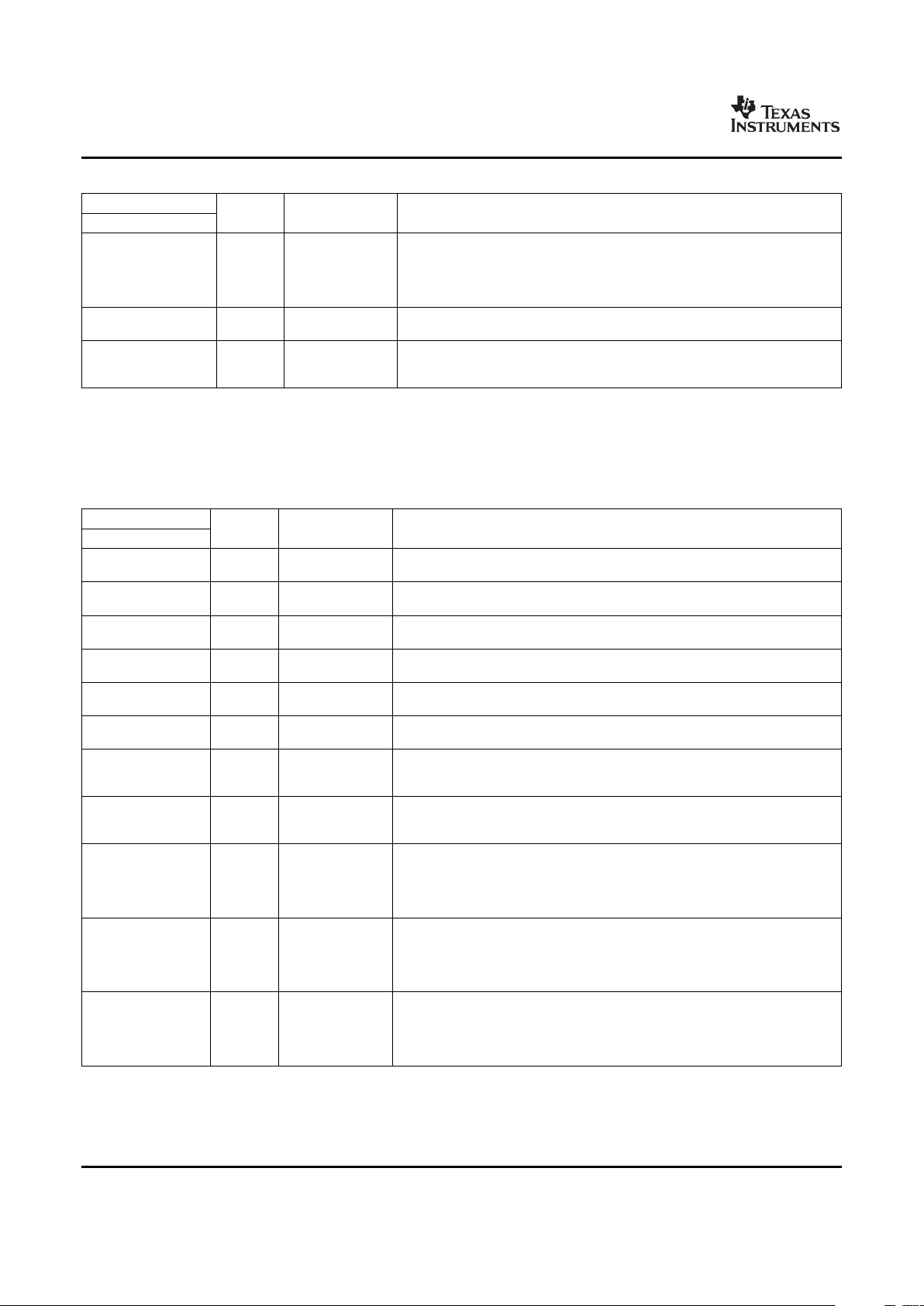
www.ti.com
PRODUCT PREVIEW
2.4.6 Multi-Media Card/Secure Digital (MMC/SD) Interfaces
TMS320DM355
Digital Media System-on-Chip (DMSoC)
SPRS463 – SEPTEMBER 2007
Table 2-11. GPIO Terminal Functions (continued)
TERMINAL
TYPE
(1)
OTHER
(2) (3)
DESCRIPTION
NAME NO.
Standard CCD Analog Front End (AFE): NOT USED YCC 16-bit: time
CIN7 /
multiplexed between chroma: CB/CR[07] YCC 08-bit (which allows for 2
GIO101 / PD
N3 I/O/Z simultaneous decoder inputs), it is time multiplexed between luma and chroma of
SPI2_SCL V
DD_VIN
the upper channel. Y/CB/CR[07] SPI: SPI2 Clock
K
GIO: GIO[101]
SPI0_SDI SPI0: Data In
A12 I/O/Z V
DD
/ GIO102 GIO: GIO[102]
SPI0_SDE
SPI0: Chip Select 0
NA[0] / B12 I/O/Z V
DD
GIO: GIO[103]
GIO103
The DM355 includes two Multi-Media Card/Secure Digital card interfaces that are compatible with the
MMC/SD and SDIO protocol.
Table 2-12. MMC/SD Terminal Functions
TERMINAL
TYPE
(1)
OTHER
(2) (3)
DESCRIPTION
NAME NO.
MMCSD0_
A15 I/O/Z V
DD
MMCSD0: Clock
CLK/
MMCSD0_
C14 I/O/Z V
DD
MMCSD0: Command
CMD/
MMCSD0_
B14 I/O/Z V
DD
MMCSD0: DATA0
DATA0/
MMCSD0_
D14 I/O/Z V
DD
MMCSD0: DATA1
DATA1/
MMCSD0_
B13 I/O/Z V
DD
MMCSD0: DATA2
DATA2/
MMCSD0_
A14 I/O/Z V
DD
MMCSD0: DATA3
DATA3/
MMCSD1_
MMCSD1: Clock
CLK/ C15 I/O/Z V
DD
GIO: GIO[024]
GIO024
MMCSD1_
MMCSD1: Command
CMD/ A17 I/O/Z V
DD
GIO: GIO[023]
GIO023
MMCSD1_
DATA0/ MMCSD1: DATA0
GIO019/ A18 I/O/Z V
DD
GIO: GIO[019]
UART2_T UART2: Transmit data
XD
MMCSD1_
DATA1/ MMCSD1: DATA1
GIO020/ B15 I/O/Z V
DD
GIO: GIO[020]
UART2_R UART2: Receive data
XD
MMCSD1_
DATA2/ MMCSD1: DATA2
GIO021/ A16 I/O/Z V
DD
GIO: GIO[021]
UART2_C UART2: CTS
TS
(1) I = Input, O = Output, Z = High impedance, S = Supply voltage, GND = Ground, A = Analog signal.
(2) Specifies the operating I/O supply voltage for each signal. See Section 5.3 , Power Supplies for more detail.
(3) PD = pull-down, PU = pull-up. (To pull up a signal to the opposite supply rail, a 1 k Ω resistor should be used.)
Device Overview28 Submit Documentation Feedback
Page 29
www.ti.com
2.4.7 Universal Serial Bus (USB) Interface
TMS320DM355
Digital Media System-on-Chip (DMSoC)
SPRS463 – SEPTEMBER 2007
Table 2-12. MMC/SD Terminal Functions (continued)
TERMINAL
TYPE
(1)
OTHER
(2) (3)
DESCRIPTION
NAME NO.
MMCSD1_
DATA3/ MMCSD1: DATA3
GIO022/ B16 I/O/Z V
DD
GIO: GIO[022]
UART2_R UART2: RTS
TS
The Universal Serial Bus (USB) interface supports the USB2.0 High-Speed protocol and includes dual-role
Host/Slave support. However, no charge pump is included.
NOTE
OTG supplies are not supported. Please ignore all references to OTG in this document.
Table 2-13. USB Terminal Functions
TERMINAL
TYPE
(1)
OTHER
(2) (3)
DESCRIPTION
NAME NO.
USB D+ (differential signal pair).
USB_DP A7 A I/O/Z V
DDA33_USB
When USB is not used, this signal should be connected to V
SS_USB
.
USB D- (differential signal pair).
USB_DM A6 A I/O/Z V
DDA33_USB
When USB is not used, this signal should be connected to V
SS_USB
.
USB reference current output
Connect to VSS_USB_REF via 10K ohm , 1% resistor placed as close to the
USB_R1 C7 A I/O/Z
device as possible.
When USB is not used, this signal should be connected to V
SS_USB
.
USB operating mode identification pin
For Device mode operation only, pull up this pin to VDD with a 1.5K ohm resistor.
For Host mode operation only, pull down this pin to ground (VSS) with a 1.5K
USB_ID D5 A I/O/Z V
DDA33_USB
ohm resistor.
If using an OTG or mini-USB connector, this pin will be set properly via the
cable/connector configuration.
When USB is not used, this signal should be connected to V
SS_USB
.
For host or device mode operation, tie the VBUS/USB power signal to the USB
connector.
USB_VBUS E5 A I/O/Z V
DD
When used in OTG mode operation, tie VBUS to the external charge pump and
to the VBUS signal on the USB connector.
When the USB is not used, tie VBUS to Vss_USB.
Digital output to control external 5 V supply
USB_DRVVBUS C5 O/Z V
DD
When USB is not used, this signal should be left as a No Connect.
USB Ground Reference
V
SS_USB_REF
C8 GND V
DD
Connect directly to ground and to USB_R1 via 10K ohm, 1% resistor placed as
close to the device as possible
Analog 3.3 V power USBPHY
V
DDA3P3_USB
J8 PWR V
DD
When USB is not used, this signal should be connected to V
SS_USB
.
Common mode 3.3 V power for USB PHY
V
DDACM3P3_USB
B6 PWR V
DD
When USB is not used, this signal should be connected to V
SS_USB
.
Analog 1.2 V power for USB PHY
V
DDA1P2_USB
H7 PWR V
DD
When USB is not used, this signal should be connected to V
SS_USB
.
Digital 1.2 V power for USB PHY
V
DDD1P2_USB
C6 PWR V
DD
When USB is not used, this signal should be connected to V
SS_USB
.
(1) I = Input, O = Output, Z = High impedance, S = Supply voltage, GND = Ground, A = Analog signal.
(2) Specifies the operating I/O supply voltage for each signal. See Section 5.3 , Power Supplies for more detail.
(3) PD = pull-down, PU = pull-up. (To pull up a signal to the opposite supply rail, a 1 k Ω resistor should be used.)
Submit Documentation Feedback Device Overview 29
Page 30
www.ti.com
PRODUCT PREVIEW
2.4.8 Audio Interfaces
2.4.9 UART Interface
TMS320DM355
Digital Media System-on-Chip (DMSoC)
SPRS463 – SEPTEMBER 2007
The DM355 includes two Audio Serial Ports (ASP ports), which are backward compatible with other TI
ASP serial ports and provide I2S audio interface. One interface is multiplexed with GIO signals.
Table 2-14. ASP Terminal Functions
TERMINAL
TYPE
(1)
OTHER
(2) (3)
DESCRIPTION
NAME NO.
ASP0_CL
ASP0: Receive Clock
KR/ F17 I/O/Z V
DD
GIO: GIO[026]
GIO26
ASP0_CL
ASP0: Transmit Clock
KX / F18 I/O/Z V
DD
GIO: GIO[029]
GIO029
ASP0_DR
ASP0: Receive DataF
/ E18 I/O/Z V
DD
GIO: GIO[027]
GIO027
ASP0_DX
ASP0: Transmit Data
/ H15 I/O/Z V
DD
GIO: GIO[030]
GIO030
ASP0_FS
ASP0: Receive Frame Synch
R / F16 I/O/Z V
DD
GIO: GIO[025]
GIO025
ASP0_FS
X / G17 I/O/Z V
DD
ASP0: Transmit Frame SynchGIO: GIO[028]
GIO028
ASP1_CL
D18 I/O/Z V
DD
ASP1: Receive Clock
KR
ASP1_CL
D17 I/Z V
DD
ASP1: Master Clock
KS
ASP1_CL
D19 I/O/Z V
DD
ASP1: Transmit Clock
KX
ASP1_DR C19 I/O/Z V
DD
ASP1: Receive Data
ASP1_DX C18 I/O/Z V
DD
ASP1: Transmit Data
ASP1_FS
E17 I/O/Z V
DD
ASP1: Receive Frame Synch
R
ASP1_FS
E16 I/O/Z V
DD
ASP1: Transmit Frame Sync
X
(1) I = Input, O = Output, Z = High impedance, S = Supply voltage, GND = Ground, A = Analog signal.
(2) Specifies the operating I/O supply voltage for each signal. See Section 5.3 , Power Supplies for more detail.
(3) PD = pull-down, PU = pull-up. (To pull up a signal to the opposite supply rail, a 1 k Ω resistor should be used.)
The includes three UART ports. These ports are multiplexed with GIO and other signals.
Table 2-15. UART Terminal Functions
TERMINAL
TYPE
(1)
OTHER
(2) (3)
DESCRIPTION
NAME NO.
UART0_RXD U18 I V
DD
UART0: Receive data. Used for UART boot mode
UART0_TXD T18 O V
DD
UART0: Transmit data. Used for UART boot mode
UART1_RXD UART1: Receive data.
R15 I/O/Z V
DD
GIO013 GIO: GIO013
UART1_TXD UART1: Transmit data.
R17 I/O/Z V
DD
GIO012 GIO: GIO012
(1) I = Input, O = Output, Z = High impedance, S = Supply voltage, GND = Ground, A = Analog signal.
(2) Specifies the operating I/O supply voltage for each signal. See Section 5.3 , Power Supplies for more detail.
(3) PD = pull-down, PU = pull-up. (To pull up a signal to the opposite supply rail, a 1 k Ω resistor should be used.)
Device Overview30 Submit Documentation Feedback
Page 31
www.ti.com
2.4.10 I2C Interface
2.4.11 Serial Interface
TMS320DM355
Digital Media System-on-Chip (DMSoC)
SPRS463 – SEPTEMBER 2007
Table 2-15. UART Terminal Functions (continued)
TERMINAL
TYPE
(1)
OTHER
(2) (3)
DESCRIPTION
NAME NO.
MMCSD1_DA
MMCSD1: DATA2
TA2/
A16 I/O/Z V
DD
GIO: GIO021
GIO021
UART2: CTS
UART2_CTS
MMCSD1_DA
MMCSD1: DATA3
TA3/
B16 I/O/Z V
DD
GIO: GIO022
GIO022
UART2: RTS
UART2_RTS
MMCSD1_DA
MMCSD1: DATA1
TA1/
B15 I/O/Z V
DD
GIO: GIO020
GIO020
UART2: RXD
UART2_RXD
MMCSD1_DA
MMCSD1: DATA0
TA0/
A18 I/O/Z V
DD
GIO: GIO019
GIO019
UART2: TXD
UART2_TXD
The includes an I2C two-wire serial interface for control of external peripherals. This interface is
multiplexed with GIO signals.
Table 2-16. I2C Terminal Functions
TERMINAL
TYPE
(1)
OTHER
(2) (3)
DESCRIPTION
NAME NO.
I2C_SDA/ I2C: Serial data
R13 I/O/Z V
DD
GIO015 GIO: GIO015
I2C_SCL/ I2C: Serial clock
R14 I/O/Z V
DD
GIO014 GIO: GIO014
(1) I = Input, O = Output, Z = High impedance, S = Supply voltage, GND = Ground, A = Analog signal.
(2) Specifies the operating I/O supply voltage for each signal. See Section 5.3 , Power Supplies for more detail.
(3) PD = pull-down, PU = pull-up. (To pull up a signal to the opposite supply rail, a 1 k Ω resistor should be used.)
The includes three independent serial ports. These interfaces are multiplexed with GIO and other signals.
Table 2-17. SPI Terminal Functions
TERMINAL
TYPE
(1)
OTHER
(2) (3)
DESCRIPTION
NAME NO.
SPI0_SCLK C12 I/O/Z V
DD
SPI0: Clock
SPI0_SDENA[0]/ SPI0: Chip select 0
B12 I/O/Z V
DD
GIO103 GIO: GIO[103]
GIO007 GIO: GIO[007]
B12 I/O/Z V
DD
SPI0_SDENA[1] SPI0: Chip select 1
SPI0_SDI/ SPI0: Data in
A12 I/O/Z V
DD
GIO102 GIO: GIO[102]
SPI0_SDO B11 I/O/Z V
DD
SPI0: Data out
SPI1_SCLK/ SPI1: Clock
C13 I/O/Z V
DD
GIO010 GIO: GIO[010]
SPI1: Chip select 0
SPI1_SDENA[0]/
E13 I/O/Z V
DD
GIO: GIO[011] - Active low during MMC/SD boot (can be used as
GIO011
MMC/SD power control)
(1) I = Input, O = Output, Z = High impedance, S = Supply voltage, GND = Ground, A = Analog signal.
(2) Specifies the operating I/O supply voltage for each signal. See Section 5.3 , Power Supplies for more detail.
(3) PD = pull-down, PU = pull-up. (To pull up a signal to the opposite supply rail, a 1 k Ω resistor should be used.)
Submit Documentation Feedback Device Overview 31
Page 32

www.ti.com
PRODUCT PREVIEW
2.4.12 Clock Interface
TMS320DM355
Digital Media System-on-Chip (DMSoC)
SPRS463 – SEPTEMBER 2007
Table 2-17. SPI Terminal Functions (continued)
TERMINAL
TYPE
(1)
OTHER
(2) (3)
DESCRIPTION
NAME NO.
SPI1_SDI SPI1: Data in or
GIO009 A13 I/O/Z V
DD
SPI1: Chip select
SPI1_SDENA[1] GIO: GIO[09]
SPI1_SDO SPI1: Data out
E12 I/O/Z V
DD
GIO008 GIO: GIO[008]
Standard CCD Analog Front End (AFE): Not used
• YCC 16-bit: time multiplexed between chroma. CB/CR[07]
CIN7/
• YCC 8-bit (which allows for two simultaneous decoder inputs), it is
PD
GIO101/ N3 I/O/Z
time multiplexed between luma and chroma of the upper channel.
V
DD_VIN
SPI2_SCLK
Y/CB/CR[07]
SPI: SPI2 clock
GIO: GIO[101]
Standard CCD Analog Front End (AFE): Raw[13]
• YCC 16-bit: time multiplexed between chroma. CB/CR[05]
CIN5/
• YCC 8-bit (which allows for two simultaneous decoder inputs), it is
PD
GIO099/ M3 I/O/Z
time multiplexed between luma and chroma of the upper channel.
V
DD_VIN
SPI2_SDENA[0]
Y/CB/CR[07]
SPI: SPI2 chip select
GIO: GIO[099]
Standard CCD Analog Front End (AFE): Raw[12]
• YCC 16-bit: time multiplexed between chroma. CB/CR[04]
CIN4/
• YCC 8-bit (which allows for two simultaneous decoder inputs), it is
GIO098/ PD
L4 I/O/Z
time multiplexed between luma and chroma of the upper channel.
SPI2_SDI/ V
DD_VIN
Y/CB/CR[04]
SPI2_SDENA[1]
SPI: SPI2 Data in
GIO: GIO[0998]
Standard CCD Analog Front End (AFE): Not used
• YCC 16-bit: time multiplexed between chroma. CB/CR[06]
CIN6/
• YCC 8-bit (which allows for two simultaneous decoder inputs), it is
PD
GIO100/ K5 I/O/Z
time multiplexed between luma and chroma of the upper channel.
V
DD_VIN
SPI2_SDO/
Y/CB/CR[06]
SPI: SPI2 Data out
GIO: GIO[100]
The provides interface with the system clocks.
Table 2-18. Clocks Terminal Functions
TERMINAL
TYPE
(1)
OTHER
(2) (3)
DESCRIPTION
NAME NO.
CLKOUT1 CLKOUT: Output Clock 1
D12 I/O/Z V
DD
/ GIO018 GIO: GIO[018]
CLKOUT2 CLKOUT: Output Clock 2
A11 I/O/Z V
DD
/ GIO017 GIO: GIO[017]
CLKOUT3 CLKOUT: Output Clock 3
C11 I/O/Z V
DD
/ GIO016 GIO: GIO[016]
MXI1 A9 I V
DD
Crystal input for system oscillator (24 MHz or 36 MHz)
Output for system oscillator (24 MHz or 36 MHz). When the MX02 is not used,
MXO1 B9 O V
DD
the MX02 signal can be left open.
Crystal input for video oscillator (27 MHz) Optional, use only if 27MHz derived
from MXI1 and PLL does not provide sufficient performance for Video DAC.
MXI2 R1 I V
DD
When the MX12 is not used and powered down, the MXI2 signal should be left
as a No Connect
(1) I = Input, O = Output, Z = High impedance, S = Supply voltage, GND = Ground, A = Analog signal.
(2) Specifies the operating I/O supply voltage for each signal. See Section 5.3 , Power Supplies for more detail.
(3) PD = pull-down, PU = pull-up. (To pull up a signal to the opposite supply rail, a 1 k Ω resistor should be used.)
Device Overview32 Submit Documentation Feedback
Page 33

www.ti.com
2.4.13 Real Time Output (RTO) Interface
2.4.14 Pulse Width Modulator (PWM) Interface
TMS320DM355
Digital Media System-on-Chip (DMSoC)
SPRS463 – SEPTEMBER 2007
Table 2-18. Clocks Terminal Functions (continued)
TERMINAL
TYPE
(1)
OTHER
(2) (3)
DESCRIPTION
NAME NO.
Output for video oscillator (27 MHz) Optional, use only if 27MHz derived from
MXI1 and PLL does not provide sufficient performance for Video DAC When the
MXO2 T1 O V
DD
MXO2 is not used and powered down, the MXO2 signal should be left as a No
Connect.
The provides Real Time Output (RTO) interface.
Table 2-19. RTO Terminal Functions
TERMINAL
TYPE
(1)
OTHER
(2) (3)
DESCRIPTION
NAME NO.
COUT5G2 / Digital Video Out: VENC settings determine function GIO: GIO[079]
GIO079 / C1 I/O/Z V
DD_VOUT
PWM2A
PWM2A / RTO0
RTO0
COUT4B7 / Digital Video Out: VENC settings determine function GIO: GIO[078]
GIO078 / D3 I/O/Z V
DD_VOUT
PWM2B
PWM2B / RTO1
RTO1
COUT3B6 / Digital Video Out: VENC settings determine function GIO: GIO[077]
GIO077 / E3 I/O/Z V
DD_VOUT
PWM2C
PWM2C / RTO2
RTO2
COUT2B5 / Digital Video Out: VENC settings determine function GIO: GIO[076]
GIO076 / E4 I/O/Z V
DD_VOUT
PWM2D
PWM2D / RTO3
RTO3
(1) I = Input, O = Output, Z = High impedance, S = Supply voltage, GND = Ground, A = Analog signal.
(2) Specifies the operating I/O supply voltage for each signal. See Section 5.3 , Power Supplies for more detail.
(3) PD = pull-down, PU = pull-up. (To pull up a signal to the opposite supply rail, a 1 k Ω resistor should be used.)
The provides Pulse Width Modulator (PWM) interface.
Table 2-20. PWM Terminal Functions
TERMINAL
TYPE
(1)
OTHER
(2) (3)
DESCRIPTION
NAME NO.
COUT7G4 / Digital Video Out: VENC settings determine function GIO: GIO[081]
C2 I/O/Z V
DD_VOUT
GIO081 / PWM0
PWM0
COUT6G3 / Digital Video Out: VENC settings determine function GIO: GIO[080]
D2 I/O/Z V
DD_VOUT
GIO080 / PWM1
PWM1
(1) I = Input, O = Output, Z = High impedance, S = Supply voltage, GND = Ground, A = Analog signal.
(2) Specifies the operating I/O supply voltage for each signal. See Section 5.3 , Power Supplies for more detail.
(3) PD = pull-down, PU = pull-up. (To pull up a signal to the opposite supply rail, a 1 k Ω resistor should be used.)
Submit Documentation Feedback Device Overview 33
Page 34
www.ti.com
PRODUCT PREVIEW
2.4.15 System Configuration Interface
TMS320DM355
Digital Media System-on-Chip (DMSoC)
SPRS463 – SEPTEMBER 2007
Table 2-20. PWM Terminal Functions (continued)
TERMINAL
TYPE
(1)
OTHER
(2) (3)
DESCRIPTION
NAME NO.
COUT5G2 / Digital Video Out: VENC settings determine function GIO: GIO[079]
GIO079 / C1 I/O/Z V
DD_VOUT
PWM2A
PWM2A / RTO0
RTO0
COUT4B7 / Digital Video Out: VENC settings determine function GIO: GIO[078]
GIO078 / D3 I/O/Z V
DD_VOUT
PWM2B
PWM2B / RTO1
RTO1
COUT3B6 / Digital Video Out: VENC settings determine function GIO: GIO[077]
GIO077 / E3 I/O/Z V
DD_VOUT
PWM2C
PWM2C / RTO2
RTO2
COUT2B5 / Digital Video Out: VENC settings determine function GIO: GIO[076]
GIO076 / E4 I/O/Z V
DD_VOUT
PWM2D
PWM2D / RTO3
RTO3
COUT1B4 / Digital Video Out: VENC settings determine function GIO: GIO[075]
F3 I/O/Z V
DD_VOUT
GIO075 / PWM3A
PWM3A
COUT0B3 / Digital Video Out: VENC settings determine function GIO: GIO[074]
F4 I/O/Z V
DD_VOUT
GIO074 / PWM3B
PWM3B
FIELD /
Video Encoder: Field identifier for interlaced display formats GIO: GIO[070]
GIO070 /
H4 I/O/Z V
DD_VOUT
Digital Video Out: R2
R2 /
PWM3C
PWM3C
EXTCLK /
Video Encoder: External clock input, used if clock rates > 27 MHz are needed,
GIO069 / PD
G3 I/O/Z e.g. 74.25 MHz for HDTV digital output GIO: GIO[069] Digital Video Out: B2
B2 / V
DD_VOUT
PWM3D
PWM3D
The provides interfaces for system configuration and boot load.
Table 2-21. System/Boot Terminal Functions
TERMINAL
TYPE
(1)
OTHER
(2) (3)
DESCRIPTION
NAME NO.
Async EMIF: Address bus bit 13
EM_A13/
PD GIO: GIO[067]
GOP067/ V19 I/O/Z
V
DD
System: BTSEL[1:0] sampled at power-on-reset to determine boot method. Used
BTSEL[1]
to drive boot status LED signal (active low) in ROM boot modes.
EM_A12/ Async EMIF: Address bus bit 12
PD
GOP066/ U19 I/O/Z GIO: GIO[066]
V
DD
BTSEL[0] System: BTSEL[1:0] sampled at power-on-reset to determine boot method.
Async EMIF: Address bus bit 11
EM_A11/ GIO: GIO[065]
PU
GOP065/ R16 I/O/Z System: AECFG[3:0] sampled a power-on-reset to set AEMIF configuration.
V
DD
AECFG[3] AECFG[3] sets default fo PinMux2.EM_D15_8. AEMIF default bus width (16 or 8
bits).
(1) I = Input, O = Output, Z = High impedance, S = Supply voltage, GND = Ground, A = Analog signal.
(2) Specifies the operating I/O supply voltage for each signal. See Section 5.3 , Power Supplies for more detail.
(3) PD = pull-down, PU = pull-up. (To pull up a signal to the opposite supply rail, a 1 k Ω resistor should be used.)
Device Overview34 Submit Documentation Feedback
Page 35

www.ti.com
2.4.16 Emulation
TMS320DM355
Digital Media System-on-Chip (DMSoC)
SPRS463 – SEPTEMBER 2007
Table 2-21. System/Boot Terminal Functions (continued)
TERMINAL
TYPE
(1)
OTHER
(2) (3)
DESCRIPTION
NAME NO.
Async EMIF: Address bus bit 10
EM_A10/ GIO: GIO[064]
PU
GOP064/ R18 I/O/Z System: AECFG[3:0] sampled a power-on-reset to set AEMIF configuration.
V
DD
AECFG[2] AECFG[2:1] sets default fo PinMux2.EM_BA0. AEMIF EM_BA0 definition:
(EM,_BA0, EM_A14, GOP[054], rsvd)
Async EMIF: Address bus bit 09
EM_A09/ GIO: GIO[063]
PD
GOP063/ P17 I/O/Z System: AECFG[3:0] sampled a power-on-reset to set AEMIF configuration.
V
DD
AECFG[1] AECFG[2:1] sets default fo PinMux2.EM_BA0. AEMIF EM_BA0 definition:
(EM,_BA0, EM_A14, GOP[054], rsvd)
Async EMIF: Address bus bit 08
GIO: GIO[062]
EM_A08/
PD
System: AECFG[0] sets default for:
GOP062/ T19 I/O/Z
V
DD
AECFG[0] • PinMux2.EM_A0_BA1 - AEMIF address width (OneNAND, or NAND)
• PinMux2.EM_A13_3 - AEMIF address width (OneNAND, or NAND)
The emulation interface allow software and hardware debugging.
Table 2-22. Emulation Terminal Functions
TERMINAL
TYPE
(1)
OTHER
(2) (3)
DESCRIPTION
NAME NO.
TCK E10 I V
DD
JTAG test clock input
PU
TDI D9 I JTAG test data input
V
DD
TDO E9 O V
DD
JTAG test data output
PU
TMS D8 I JTAG test mode select
V
DD
PD
TRST C9 I JTAG test logic reset (active low)
V
DD
RTCK E11 O V
DD
JTAG test clock output
JTAG emulation 0 I/O
PU
EMU0 E8 I/O/Z EMU[1:0] = 00 - Force Debug Scan chain (ARM and ARM ETB TAPs connected)
V
DD
EMU[1:0] = 11 - Normal Scan chain (ICEpick only)
JTAG emulation 1 I/O
PU
EMU1 E7 I/O/Z EMU[1:0] = 00 - Force Debug Scan chain (ARM and ARM ETB TAPs connected)
V
DD
EMU[1:0] = 11 - Normal Scan chain (ICEpick only)
(1) I = Input, O = Output, Z = High impedance, S = Supply voltage, GND = Ground, A = Analog signal.
(2) Specifies the operating I/O supply voltage for each signal. See Section 5.3 , Power Supplies for more detail.
(3) PD = pull-down, PU = pull-up. (To pull up a signal to the opposite supply rail, a 1 k Ω resistor should be used.)
Submit Documentation Feedback Device Overview 35
Page 36

www.ti.com
PRODUCT PREVIEW
2.5 Pin List
TMS320DM355
Digital Media System-on-Chip (DMSoC)
SPRS463 – SEPTEMBER 2007
Table 2-23 provides a complete pin description list in pin number order.
Table 2-23. DM355 Pin Descriptions
Name Pin BGA Type Grou Power PU Reset Description
(4)
Mux Control
# ID
(1)
p Supply
(2)
PD
(3
State
)
CIN7 / GIO101 1 N3 I/O CCDC V
DD_VIN
PD in Standard CCD Analog Front End (AFE): PINMUX0[1:0].CIN
/ SPI2_SCLK / GIO / NOT USED _7
SPI2
YCC 16-bit: time multiplexed between
chroma: CB/CR[07]
YCC 08-bit (which allows for 2
simultaneous decoder inputs), it is time
multiplexed between
luma and chroma of the upper channel.
Y/CB/CR[07]
SPI: SPI2 Clock
GIO: GIO[101]
CIN6 / GIO100 2 K5 I/O CCDC V
DD_VIN
PD in Standard CCD Analog Front End (AFE): PINMUX0[3:2].CIN
/ SPI2_SDO / GIO / NOT USED _6
SPI2
YCC 16-bit: time multiplexed between
chroma: CB/CR[06]
YCC 08-bit (which allows for 2
simultaneous decoder inputs), it is time
multiplexed between luma and chroma of
the upper channel. Y/CB/CR[06]
SPI: SPI2 Data Out
GIO: GIO[100]
CIN5 / GIO099 3 M3 I/O CCDC V
DD_VIN
PD in Standard CCD Analog Front End (AFE): PINMUX0[5:4].CIN
/ / GIO / raw[13] _5
SPI2_SDENA[ SPI2
0]
YCC 16-bit: time multiplexed between
chroma: CB/CR[05]
YCC 08-bit (which allows for 2
simultaneous decoder inputs), it is time
multiplexed between luma and chroma of
the upper channel. Y/CB/CR[05]
SPI: SPI2 Chip Select
GIO: GIO[99]
CIN4 / GIO098 4 L4 I/O CCDC V
DD_VIN
PD in Standard CCD Analog Front End (AFE): PINMUX0[7:6].CIN
/ SPI2_SDI / / GIO / raw[12] _4
SPI2_SDENA[ SPI2 /
1] SPI2
YCC 16-bit: time multiplexed between
chroma: CB/CR[04]
YCC 08-bit (which allows for 2
simultaneous decoder inputs), it is time
multiplexed between luma and chroma of
the upper channel. Y/CB/CR[04]
SPI: SPI2 Data In
GIO: GIO[098]
(1) I = Input, O = Output, Z = High impedance, S = Supply voltage, GND = Ground, A = Analog signal.
(2) Specifies the operating I/O supply voltage for each signal. See Section 5.3 , Power Supplies for more detail.
(3) PD = pull-down, PU = pull-up. (To pull up a signal to the opposite supply rail, a 1 k Ω resistor should be used.)
(4) To reduce EMI and reflections, depending on the trace length, approximately 22 Ω to 50 Ω damping resistors are recommend on the
following outputs placed near the DM355: YOUT(0-7),COUT(0-7), HSYNC,VSYNC,LCD_OE,FIELD,EXTCLK,VCLK. The trace lengths
should be minimized.
Device Overview36 Submit Documentation Feedback
Page 37

www.ti.com
TMS320DM355
Digital Media System-on-Chip (DMSoC)
SPRS463 – SEPTEMBER 2007
Table 2-23. DM355 Pin Descriptions (continued)
Name Pin BGA Type Grou Power PU Reset Description
(4)
Mux Control
# ID
(1)
p Supply
(2)
PD
(3
State
)
CIN3 / GIO097 5 J4 I/O CCDC V
DD_VIN
PD in Standard CCD Analog Front End (AFE): PINMUX0[8].CIN_
/ GIO raw[11] 32
YCC 16-bit: time multiplexed between
chroma: CB/CR[03]
YCC 08-bit (which allows for 2
simultaneous decoder inputs), it is time
multiplexed between luma and chroma of
the upper channel. Y/CB/CR[03]
GIO: GIO[097]
CIN2 / GIO096 6 J5 I/O CCDC V
DD_VIN
PD in Standard CCD Analog Front End (AFE): PINMUX0[8].CIN_
/ GIO raw[10] 32
YCC 16-bit: time multiplexed between
chroma: CB/CR[02]
YCC 08-bit (which allows for 2
simultaneous decoder inputs), it is time
multiplexed between luma and chroma of
the upper channel. Y/CB/CR[02]
GIO: GIO[096]
CIN1 / GIO095 7 L3 I/O CCDC V
DD_VIN
PD in Standard CCD Analog Front End (AFE): PINMUX0[9].CIN_
/ GIO raw[09] 10
YCC 16-bit: time multiplexed between
chroma: CB/CR[01]
YCC 08-bit (which allows for 2
simultaneous decoder inputs), it is time
multiplexed between luma and chroma of
the upper channel. Y/CB/CR[01]
GIO: GIO[095]
CIN0 / GIO094 8 J3 I/O CCDC V
DD_VIN
PD in Standard CCD Analog Front End (AFE): PINMUX0[9].CIN_
/ GIO raw[08] 10
YCC 16-bit: time multiplexed between
chroma: CB/CR[00]
YCC 08-bit (which allows for 2
simultaneous decoder inputs), it is time
multiplexed between luma and chroma of
the upper channel. Y/CB/CR[00]
GIO: GIO[094]
YIN7 / GIO093 9 L5 I/O CCDC V
DD_VIN
PD in Standard CCD Analog Front End (AFE): PINMUX0[10].YIN
/ GIO raw[07] _70
YCC 16-bit: time multiplexed between
luma: Y[07]
YCC 08-bit (which allows for 2
simultaneous decoder inputs), it is time
multiplexed between luma and chroma of
the lower channel. Y/CB/CR[07]
GIO: GIO[093]
YIN6 / GIO092 10 M4 I/O CCDC V
DD_VIN
PD in Standard CCD Analog Front End (AFE): PINMUX0[10].YIN
/ GIO raw[06] _70
YCC 16-bit: time multiplexed between
luma: Y[06]
YCC 08-bit (which allows for 2
simultaneous decoder inputs), it is time
multiplexed between luma and chroma of
the lower channel. Y/CB/CR[06]
GIO: GIO[092]
Submit Documentation Feedback Device Overview 37
Page 38

www.ti.com
PRODUCT PREVIEW
TMS320DM355
Digital Media System-on-Chip (DMSoC)
SPRS463 – SEPTEMBER 2007
Table 2-23. DM355 Pin Descriptions (continued)
Name Pin BGA Type Grou Power PU Reset Description
(4)
Mux Control
# ID
(1)
p Supply
(2)
PD
(3
State
)
YIN5 / GIO091 11 M5 I/O CCDC V
DD_VIN
PD in Standard CCD Analog Front End (AFE): PINMUX0[10].YIN
/ GIO raw[05] _70
YCC 16-bit: time multiplexed between
luma: Y[05]
YCC 08-bit (which allows for 2
simultaneous decoder inputs), it is time
multiplexed between luma and chroma of
the lower channel. Y/CB/CR[05]
GIO: GIO[091]
YIN4 / GIO090 12 P3 I/O CCDC V
DD_VIN
PD in Standard CCD Analog Front End (AFE): PINMUX0[10].YIN
/ GIO raw[04] _70
YCC 16-bit: time multiplexed between
luma: Y[04]
YCC 08-bit (which allows for 2
simultaneous decoder inputs), it is time
multiplexed between luma and chroma of
the lower channel. Y/CB/CR[04]
GIO: GIO[090]
YIN3 / GIO089 13 R3 I/O CCDC V
DD_VIN
PD in Standard CCD Analog Front End (AFE): PINMUX0[10].YIN
/ GIO raw[03] _70
YCC 16-bit: time multiplexed between
luma: Y[03]
YCC 08-bit (which allows for 2
simultaneous decoder inputs), it is time
multiplexed between luma and chroma of
the lower channel. Y/CB/CR[03]
GIO: GIO[089]
YIN2 / GIO088 14 P4 I/O CCDC V
DD_VIN
PD in Standard CCD Analog Front End (AFE): PINMUX0[10].YIN
/ GIO raw[02] _70
YCC 16-bit: time multiplexed between
luma: Y[02]
YCC 08-bit (which allows for 2
simultaneous decoder inputs), it is time
multiplexed between luma and chroma of
the lower channel. Y/CB/CR[02]
GIO: GIO[088]
YIN1 / GIO087 15 P2 I/O CCDC V
DD_VIN
PD in Standard CCD Analog Front End (AFE): PINMUX0[10].YIN
/ GIO raw[01] _70
YCC 16-bit: time multiplexed between
luma: Y[01]
YCC 08-bit (which allows for 2
simultaneous decoder inputs), it is time
multiplexed between luma and chroma of
the lower channel. Y/CB/CR[01]
GIO: GIO[087]
YIN0 / GIO086 16 P5 I/O CCDC V
DD_VIN
PD in Standard CCD Analog Front End (AFE): PINMUX0[10].YIN
/ GIO raw[00] _70
YCC 16-bit: time multiplexed between
luma: Y[00]
YCC 08-bit (which allows for 2
simultaneous decoder inputs), it is time
multiplexed between luma and chroma of
the lower channel. Y/CB/CR[00]
GIO: GIO[086]
Device Overview38 Submit Documentation Feedback
Page 39

www.ti.com
TMS320DM355
Digital Media System-on-Chip (DMSoC)
SPRS463 – SEPTEMBER 2007
Table 2-23. DM355 Pin Descriptions (continued)
Name Pin BGA Type Grou Power PU Reset Description
(4)
Mux Control
# ID
(1)
p Supply
(2)
PD
(3
State
)
CAM_HD / 17 N5 I/O CCDC V
DD_VIN
PD in Horizontal synchronization signal that can PINMUX0[11].CA
GIO085 / GIO be either an input (slave mode) or an M_HD
output (master mode). Tells the CCDC
when a new line starts.
GIO: GIO[085]
CAM_VD / 18 R4 I/O CCDC V
DD_VIN
PD in Vertical synchronization signal that can PINMUX0[12].CA
GIO084 / GIO be either an input (slave mode) or an M_VD
output (master mode). Tells the CCDC
when a new frame starts.
GIO: GIO[084]
CAM_WEN_FI 19 R5 I/O CCDC V
DD_VIN
PD in Write enable input signal is used by PINMUX0[13].CA
ELD / GIO083 / GIO external device (AFE/TG) to gate the M_WEN
DDR output of the CCDC module.
Alternately, the field identification input plus
signal is used by external device
(AFE/TG) to indicate the which of two
frames is input to the CCDC module for
sensors with interlaced output. CCDC
handles 1- or 2-field sensors in hardware.
GIO: GIO[083] CCDC.MODE[7].C
CDMD &
CCDC.MODE[5].S
WEN
PCLK / 20 T3 I/O CCDC V
DD_VIN
PD in Pixel clock input (strobe for lines CI7 PINMUX0[14].PCL
GIO082 / GIO through YI0) K
GIO: GIO[082]
DP 21 J1
DN 22 K1
SP 23 L1
SN 24 M1
LVIREF 25 N2
VDDA18V_CC 26 M2
P2
VSSA_CCP2 27 K2
28
YOUT7-R7 29 C3 I/O VENC V
DD_VOUT
in Digital Video Out: VENC settings
determine function
(4)
YOUT6-R6 30 A4 I/O VENC V
DD_VOUT
in Digital Video Out: VENC settings
determine function
(4)
YOUT5-R5 31 B4 I/O VENC V
DD_VOUT
in Digital Video Out: VENC settings
determine function
(4)
YOUT4-R4 32 B3 I/O VENC V
DD_VOUT
in Digital Video Out: VENC settings
determine function
(4)
YOUT3-R3 33 B2 I/O VENC V
DD_VOUT
in Digital Video Out: VENC settings
determine function
(4)
YOUT2-G7 34 A3 I/O VENC V
DD_VOUT
in Digital Video Out: VENC settings
determine function
(4)
YOUT1-G6 35 A2 I/O VENC V
DD_VOUT
in Digital Video Out: VENC settings
determine function
(4)
YOUT0-G5 36 B1 I/O VENC V
DD_VOUT
in Digital Video Out: VENC settings
determine function
(4)
Submit Documentation Feedback Device Overview 39
Page 40

www.ti.com
PRODUCT PREVIEW
TMS320DM355
Digital Media System-on-Chip (DMSoC)
SPRS463 – SEPTEMBER 2007
Table 2-23. DM355 Pin Descriptions (continued)
Name Pin BGA Type Grou Power PU Reset Description
(4)
Mux Control
# ID
(1)
p Supply
(2)
PD
(3
State
)
COUT7-G4 / 37 C2 I/O VENC V
DD_VOUT
in Digital Video Out: VENC settings PINMUX1[1:0].CO
GIO081 / / GIO / determine function UT_7
PWM0 PWM
0
GIO: GIO[081]
PWM0
COUT6-G3 / 38 D2 I/O VENC V
DD_VOUT
in Digital Video Out: VENC settings PINMUX1[3:2].CO
GIO080 / / GIO / determine function UT_6
PWM1 PWM
1
GIO: GIO[080]
PWM1
(4)
COUT5-G2 / 39 C1 I/O VENC V
DD_VOUT
in Digital Video Out: VENC settings PINMUX1[5:4].CO
GIO079 / / GIO / determine function UT_5
PWM2A / PWM
RTO0 2 /
RTO
GIO: GIO[079]
PWM2A
RTO0
(4)
COUT4-B7 / 40 D3 I/O VENC V
DD_VOUT
in Digital Video Out: VENC settings PINMUX1[7:6].CO
GIO078 / / GIO / determine function UT_4
PWM2B / PWM
RTO1 2 /
RTO
GIO: GIO[078]
PWM2B
RTO1
(4)
COUT3-B6 / 41 E3 I/O VENC V
DD_VOUT
in Digital Video Out: VENC settings PINMUX1[9:8].CO
GIO077 / / GIO / determine function UT_3
PWM2C / PWM
RTO2 2 /
RTO
GIO: GIO[077]
PWM2C
RTO2
(4)
COUT2-B5 / 42 E4 I/O VENC V
DD_VOUT
in Digital Video Out: VENC settings PINMUX1[11:10].C
GIO076 / / GIO / determine function OUT_2
PWM2D / PWM
RTO3 2 /
RTO
GIO: GIO[076]
PWM2D
RTO3
(4)
COUT1-B4 / 43 F3 I/O VENC V
DD_VOUT
in Digital Video Out: VENC settings PINMUX1[13:12].C
GIO075 / / GIO / determine function OUT_1
PWM3A PWM
3
GIO: GIO[075]
PWM3A
(4)
Device Overview40 Submit Documentation Feedback
Page 41

www.ti.com
TMS320DM355
Digital Media System-on-Chip (DMSoC)
SPRS463 – SEPTEMBER 2007
Table 2-23. DM355 Pin Descriptions (continued)
Name Pin BGA Type Grou Power PU Reset Description
(4)
Mux Control
# ID
(1)
p Supply
(2)
PD
(3
State
)
COUT0-B3 / 44 F4 I/O VENC V
DD_VOUT
in Digital Video Out: VENC settings PINMUX1[15:14].C
GIO074 / / GIO / determine function OUT_0
PWM3B PWM
3
GIO: GIO[074]
PWM3B
(4)
HSYNC / 45 F5 I/O VENC V
DD_VOUT
PD in Video Encoder: Horizontal Sync PINMUX1[16].HVS
GIO073 / GIO YNC
GIO: GIO[073]
(4)
VSYNC / 46 G5 I/O VENC V
DD_VOUT
PD in Video Encoder: Vertical Sync PINMUX1[16].HVS
GIO072 / GIO YNC
GIO: GIO[072]
(4)
VVALID / 47 H5 I/O VENC V
DD_VOUT
in Video Encoder: LCD Output Enable or PINMUX1[17].DLC
GIO071 / GIO BRIGHT signal D
GIO: GIO[071]
(4)
FIELD / 48 H4 I/O VENC V
DD_VOUT
in Video Encoder: Field identifier for PINMUX1[19:18].F
GIO070 / R2 / / GIO / interlaced display formats IELD
PWM3C VENC
/
PWM
3
GIO: GIO[070]
Digital Video Out: R2
PWM3C
(4)
EXTCLK / 49 G3 I/O VENC V
DD_VOUT
PD in Video Encoder: External clock input, PINMUX1[21:20].E
GIO069 / B2 / / GIO / used if clock rates > 27 MHz are needed, XTCLK
PWM3D VENC e.g. 74.25 MHz for HDTV digital output
/
PWM
3
GIO: GIO[069]
Digital Video Out: B2
PWM3D
(4)
VCLK / 50 H3 I/O VENC V
DD_VOUT
out L Video Encoder: Video Output Clock PINMUX1[22].VCL
GIO068 / GIO K
GIO: GIO[068]
(4)
VREF 51 J7 A I/O Video Video DAC: Reference voltage output
DAC (0.45V, 0.1uF to GND)
IOUT 52 E1 A I/O Video Video DAC: Pre video buffer DAC output
DAC (1000 ohm to VFB)
IBIAS 53 F2 A I/O Video Video DAC: External resistor (2550
DAC Ohms to GND) connection for current
bias configuration
VFB 54 G1 A I/O Video Video DAC: Pre video buffer DAC output
DAC (1000 ohm to IOUT, 1070 ohm to
TVOUT)
TVOUT 55 F1 A I/O Video V
DDA18_DAC
Video DAC: Analog Composite
DAC NTSC/PAL output (SeeFigure 5-31
andFigure 5-32 for circuit connection)
V
DDA18V_DAC
56 L7 PWR Video Video DAC: Analog 1.8V power
DAC
V
SSA_DAC
57 L8 GND Video Video DAC: Analog 1.8V ground
DAC
DDR_CLK 58 W9 I/O DDR V
DD_DDR
out L DDR Data Clock
Submit Documentation Feedback Device Overview 41
Page 42
www.ti.com
PRODUCT PREVIEW
TMS320DM355
Digital Media System-on-Chip (DMSoC)
SPRS463 – SEPTEMBER 2007
Table 2-23. DM355 Pin Descriptions (continued)
Name Pin BGA Type Grou Power PU Reset Description
(4)
Mux Control
# ID
(1)
p Supply
(2)
PD
(3
State
)
DDR_CLK 59 W8 I/O DDR V
DD_DDR
out H DDR Complementary Data Clock
DDR_RAS 60 T6 I/O DDR V
DD_DDR
out H DDR Row Address Strobe
DDR_CAS 61 V9 I/O DDR V
DD_DDR
out H DDR Column Address Strobe
DDR_WE 62 W10 I/O DDR V
DD_DDR
out H DDR Write Enable (active low)
DDR_CS 63 T8 I/O DDR V
DD_DDR
out H DDR Chip Select (active low)
DDR_CKE 64 V10 I/O DDR V
DD_DDR
out L DDR Clock Enable
DDR_DQM[1] 65 U15 I/O DDR V
DD_DDR
out L Data mask outputs: DQM0: For
DDR_DQ[7:0]
DDR_DQM[0] 66 T12 I/O DDR V
DD_DDR
out L Data mask outputs: DQM1: For
DDR_DQ[15:8]
DDR_DQS[1] 67 V15 I/O DDR V
DD_DDR
in Data strobe input/outputs for each byte of
the 16 bit data bus used to synchronize
the data transfers. Output to DDR when
writing and inputs when reading.
DQS1: For DDR_DQ[15:8]
DDR_DQS[0] 68 V12 I/O DDR V
DD_DDR
in Data strobe input/outputs for each byte of
the 16 bit data bus used to synchronize
the data transfers. Output to DDR when
writing and inputs when reading.
DQS0: For DDR_DQ[7:0]
DDR_BA[2] 69 V8 I/O DDR V
DD_DDR
out L Bank select outputs. Two are required for
1Gb DDR2 memories.
DDR_BA[1] 70 U7 I/O DDR V
DD_DDR
out L Bank select outputs. Two are required for
1Gb DDR2 memories.
DDR_BA[0] 71 U8 I/O DDR V
DD_DDR
out L Bank select outputs. Two are required for
1Gb DDR2 memories.
DDR_A13 72 U6 I/O DDR V
DD_DDR
out L DDR Address Bus bit 13
DDR_A12 73 V7 I/O DDR V
DD_DDR
out L DDR Address Bus bit 12
DDR_A11 74 W7 I/O DDR V
DD_DDR
out L DDR Address Bus bit 11
DDR_A10 75 V6 I/O DDR V
DD_DDR
out L DDR Address Bus bit 10
DDR_A09 76 W6 I/O DDR V
DD_DDR
out L DDR Address Bus bit 09
DDR_A08 77 W5 I/O DDR V
DD_DDR
out L DDR Address Bus bit 08
DDR_A07 78 V5 I/O DDR V
DD_DDR
out L DDR Address Bus bit 07
DDR_A06 79 U5 I/O DDR V
DD_DDR
out L DDR Address Bus bit 06
DDR_A05 80 W4 I/O DDR V
DD_DDR
out L DDR Address Bus bit 05
DDR_A04 81 V4 I/O DDR V
DD_DDR
out L DDR Address Bus bit 04
DDR_A03 82 W3 I/O DDR V
DD_DDR
out L DDR Address Bus bit 03
DDR_A02 83 W2 I/O DDR V
DD_DDR
out L DDR Address Bus bit 02
DDR_A01 84 V3 I/O DDR V
DD_DDR
out L DDR Address Bus bit 01
DDR_A00 85 V2 I/O DDR V
DD_DDR
out L DDR Address Bus bit 00
DDR_DQ15 86 W17 I/O DDR V
DD_DDR
in DDR Data Bus bit 15
DDR_DQ14 87 V16 I/O DDR V
DD_DDR
in DDR Data Bus bit 14
DDR_DQ13 88 W16 I/O DDR V
DD_DDR
in DDR Data Bus bit 13
DDR_DQ12 89 U16 I/O DDR V
DD_DDR
in DDR Data Bus bit 12
DDR_DQ11 90 W15 I/O DDR V
DD_DDR
in DDR Data Bus bit 11
DDR_DQ10 91 W14 I/O DDR V
DD_DDR
in DDR Data Bus bit 10
DDR_DQ09 92 V14 I/O DDR V
DD_DDR
in DDR Data Bus bit 09
DDR_DQ08 93 U13 I/O DDR V
DD_DDR
in DDR Data Bus bit 08
DDR_DQ07 94 W13 I/O DDR V
DD_DDR
in DDR Data Bus bit 07
Device Overview42 Submit Documentation Feedback
Page 43
www.ti.com
TMS320DM355
Digital Media System-on-Chip (DMSoC)
SPRS463 – SEPTEMBER 2007
Table 2-23. DM355 Pin Descriptions (continued)
Name Pin BGA Type Grou Power PU Reset Description
(4)
Mux Control
# ID
(1)
p Supply
(2)
PD
(3
State
)
DDR_DQ06 95 V13 I/O DDR V
DD_DDR
in DDR Data Bus bit 06
DDR_DQ05 96 W12 I/O DDR V
DD_DDR
in DDR Data Bus bit 05
DDR_DQ04 97 U12 I/O DDR V
DD_DDR
in DDR Data Bus bit 04
DDR_DQ03 98 T11 I/O DDR V
DD_DDR
in DDR Data Bus bit 03
DDR_DQ02 99 U11 I/O DDR V
DD_DDR
in DDR Data Bus bit 02
DDR_DQ01 100 W11 I/O DDR V
DD_DDR
in DDR Data Bus bit 01
DDR_DQ00 101 V11 I/O DDR V
DD_DDR
in DDR Data Bus bit 00
DDR_GATE0 102 W18 I/O DDR V
DD_DDR
DDR: Loopback signal for external DQS
gating. Route to DDR and back to
DDR_STRBEN_DEL with same
constraints as used for DDR clock and
data.
DDR_GATE1 103 V17 I/O DDR V
DD_DDR
DDR: Loopback signal for external DQS
gating. Route to DDR and back to
DDR_STRBEN with same constraints as
used for DDR clock and data.
DDR_VREF 104 U10 PWR DDRI V
DD_DDR
DDR: Voltage input for the SSTL_18 IO
O buffers
DDR_VSSDLL 105 R11 GND DDRD V
DD_DDR
DDR: Ground for the DDR DLL
LL
DDR_VDDDLL 106 R10 PWR DDRD V
DD_DDR
DDR: Power (3.3 Volts) for the DDR DLL
LL
DDR_ZN 107 T9 I/O DDRI V
DD_DDR
DDR: Reference output for drive strength
O calibration of N and P channel outputs.
Tie to ground via 50 ohm resistor @
0.5% tolerance.
EM_A13 / 108 V19 I/O AEMI V
DD
PD in L Async EMIF: Address Bus bit[13] PINMUX2[0].EM_A
GIO067 / F / 13_3,
BTSEL[1] GIO /
syste
m
GIO: GIO[067] default set by
AECFG[0]
System: BTSEL[1:0] sampled at
Power-on-Reset to determine Boot
method (00:NAND, 01:Flash, 10:UART,
11:SD)
EM_A12 / 109 U19 I/O AEMI V
DD
PD in L Async EMIF: Address Bus bit[12] PINMUX2[0].EM_A
GIO066 / F / 13_3,
BTSEL[0] GIO /
syste
m
GIO: GIO[066] default set by
AECFG[0]
System: BTSEL[1:0] sampled at
Power-on-Reset to determine Boot
method (00:NAND, 01:Flash, 10:UART,
11:SD)
Submit Documentation Feedback Device Overview 43
Page 44
www.ti.com
PRODUCT PREVIEW
TMS320DM355
Digital Media System-on-Chip (DMSoC)
SPRS463 – SEPTEMBER 2007
Table 2-23. DM355 Pin Descriptions (continued)
Name Pin BGA Type Grou Power PU Reset Description
(4)
Mux Control
# ID
(1)
p Supply
(2)
PD
(3
State
)
EM_A11 / 110 R16 I/O AEMI V
DD
PU in H Async EMIF: Address Bus bit[11] PINMUX2[0].EM_A
GIO065 / F / 13_3,
AECFG[3] GIO /
syste
m
GIO: GIO[065] default set by
AECFG[0]
System: AECFG[3:0] sampled at
Power-on-Reset to set AEMIF
Configuration
AECFG[3] sets default for
PinMux2.EM_D15_8: AEMIF Default Bus
Width (0:16 or 1:8 bits)
EM_A10 / 111 R18 I/O AEMI V
DD
PU in H Async EMIF: Address Bus bit[10] PINMUX2[0].EM_A
GIO064 / F / 13_3,
AECFG[2] GIO /
syste
m
GIO: GIO[064] default set by
AECFG[0]
System: AECFG[3:0] sampled at
Power-on-Reset to set AEMIF
Configuration
AECFG[2:1] sets default for
PinMux2.EM_BA0: AEMIF EM_BA0
Definition (00: EM_BA0, 01: EM_A14,
10:GIO[054], 11:rsvd)
EM_A09 / 112 P17 I/O AEMI V
DD
PD in L Async EMIF: Address Bus bit[09] PINMUX2[0].EM_A
GIO063 / F / 13_3,
AECFG[1] GIO /
syste
m
GIO: GIO[063] default set by
AECFG[0]
System: AECFG[3:0] sampled at
Power-on-Reset to set AEMIF
Configuration
AECFG[2:1] sets default for
PinMux2.EM_BA0: AEMIF EM_BA0
Definition (00: EM_BA0, 01: EM_A14,
10:GIO[054], 11:rsvd)
EM_A08 / 113 T19 I/O AEMI V
DD
PU in H Async EMIF: Address Bus bit[08] PINMUX2[0].EM_A
GIO062 / F / 13_3,
AECFG[0] GIO /
syste
m
GIO: GIO[062] default set by
AECFG[0]
AECFG[0] sets default for
- PinMux2.EM_A0_BA1: AEMIF Address
Width (OneNAND or NAND)
- PinMux2.EM_A13_3: AEMIF Address
Width (OneNAND or NAND)
(0:AEMIF address bits, 1:GIO[67:57])
Device Overview44 Submit Documentation Feedback
Page 45
www.ti.com
TMS320DM355
Digital Media System-on-Chip (DMSoC)
SPRS463 – SEPTEMBER 2007
Table 2-23. DM355 Pin Descriptions (continued)
Name Pin BGA Type Grou Power PU Reset Description
(4)
Mux Control
# ID
(1)
p Supply
(2)
PD
(3
State
)
EM_A07 / 114 P16 I/O AEMI V
DD
out L Async EMIF: Address Bus bit[07] PINMUX2[0].EM_A
GIO061 F / 13_3,
GIO
GIO: GIO[061] - Used by ROM default set by
Bootloader to provide progress status via AECFG[0]
LED (active low)
EM_A06 / 115 P18 I/O AEMI V
DD
out L Async EMIF: Address Bus bit[06] PINMUX2[0].EM_A
GIO060 F / 13_3,
GIO
GIO: GIO[060] default set by
AECFG[0]
EM_A05 / 116 R19 I/O AEMI V
DD
out L Async EMIF: Address Bus bit[05] PINMUX2[0].EM_A
GIO059 F / 13_3,
GIO
GIO: GIO[059] default set by
AECFG[0]
EM_A04 / 117 P15 I/O AEMI V
DD
out L Async EMIF: Address Bus bit[04] PINMUX2[0].EM_A
GIO058 F / 13_3,
GIO
GIO: GIO[058] default set by
AECFG[0]
EM_A03 / 118 N18 I/O AEMI V
DD
out L Async EMIF: Address Bus bit[03] PINMUX2[0].EM_A
GIO057 F / 13_3,
GIO
GIO: GIO[057] default set by
AECFG[0]
EM_A02 119 N15 I/O AEMI V
DD
out L Async EMIF: Address Bus bit[02]
F
NAND/SM/xD: CLE - Command Latch
Enable output
EM_A01 120 N17 I/O AEMI V
DD
out L Async EMIF: Address Bus bit[01]
F
NAND/SM/xD: ALE - Address Latch
Enable output
EM_A00 / 121 M16 I/O AEMI V
DD
out L Async EMIF: Address Bus bit[00] Note PINMUX2[1].EM_A
GIO056 F / that the EM_A0 is always a 32-bit 0_BA1,
GIO address
GIO: GIO[056] default set by
AECFG[0]
EM_BA1 / 122 P19 I/O AEMI V
DD
out H Async EMIF: Bank Address 1 signal = PINMUX2[1].EM_A
GIO055 F / 16-bit address. 0_BA1,
GIO
In 16-bit mode, lowest address bit. default set by
AECFG[0]
In 8-bit mode, second lowest address bit
GIO: GIO[055]
EM_BA0 / 123 N19 I/O AEMI V
DD
out H Async EMIF: Bank Address 0 signal = PINMUX2[3:2].EM
GIO054 / F / 8-bit address. _BA0,
EM_A14 GIO /
EMIF2
.30
In 8-bit mode, lowest address bit. default set by
AECFG[2:1]
Or, can be used as an extra Address line
(bit[14] when using 16-bit memories.
GIO: GIO[054]
Submit Documentation Feedback Device Overview 45
Page 46

www.ti.com
PRODUCT PREVIEW
TMS320DM355
Digital Media System-on-Chip (DMSoC)
SPRS463 – SEPTEMBER 2007
Table 2-23. DM355 Pin Descriptions (continued)
Name Pin BGA Type Grou Power PU Reset Description
(4)
Mux Control
# ID
(1)
p Supply
(2)
PD
(3
State
)
EM_D15 / 124 M18 I/O AEMI V
DD
in Async EMIF: Data Bus bit[15] PINMUX2[4].EM_
GIO053 F / D15_8,
GIO
GIO: GIO[053] default set by
AECFG[3]
EM_D14 / 125 M19 I/O AEMI V
DD
in Async EMIF: Data Bus bit[14] PINMUX2[4].EM_
GIO052 F / D15_8,
GIO
GIO: GIO[052] default set by
AECFG[3]
EM_D13 / 126 M15 I/O AEMI V
DD
in Async EMIF: Data Bus bit[13] PINMUX2[4].EM_
GIO051 F / D15_8,
GIO
GIO: GIO[051] default set by
AECFG[3]
EM_D12 / 127 L18 I/O AEMI V
DD
in Async EMIF: Data Bus bit[12] PINMUX2[4].EM_
GIO050 F / D15_8,
GIO
GIO: GIO[050] default set by
AECFG[3]
EM_D11 / 128 L17 I/O AEMI V
DD
in Async EMIF: Data Bus bit[11] PINMUX2[4].EM_
GIO049 F / D15_8,
GIO
GIO: GIO[049] default set by
AECFG[3]
EM_D10 / 129 L19 I/O AEMI V
DD
in Async EMIF: Data Bus bit[10] PINMUX2[4].EM_
GIO048 F / D15_8,
GIO
GIO: GIO[048] default set by
AECFG[3]
EM_D09 / 130 K18 I/O AEMI V
DD
in Async EMIF: Data Bus bit[09] PINMUX2[4].EM_
GIO047 F / D15_8,
GIO
GIO: GIO[047] default set by
AECFG[3]
EM_D08 / 131 L16 I/O AEMI V
DD
in Async EMIF: Data Bus bit[08] PINMUX2[4].EM_
GIO046 F / D15_8,
GIO
GIO: GIO[046] default set by
AECFG[3]
EM_D07 / 132 K19 I/O AEMI V
DD
in Async EMIF: Data Bus bit[07] PINMUX2[5].EM_
GIO045 F / D7_0
GIO
GIO: GIO[045]
EM_D06 / 133 K17 I/O AEMI V
DD
in Async EMIF: Data Bus bit[06] PINMUX2[5].EM_
GIO044 F / D7_0
GIO
GIO: GIO[044]
EM_D05 / 134 J19 I/O AEMI V
DD
in Async EMIF: Data Bus bit[05] PINMUX2[5].EM_
GIO043 F / D7_0
GIO
GIO: GIO[043]
EM_D04 / 135 L15 I/O AEMI V
DD
in Async EMIF: Data Bus bit[04] PINMUX2[5].EM_
GIO042 F / D7_0
GIO
GIO: GIO[042]
Device Overview46 Submit Documentation Feedback
Page 47

www.ti.com
TMS320DM355
Digital Media System-on-Chip (DMSoC)
SPRS463 – SEPTEMBER 2007
Table 2-23. DM355 Pin Descriptions (continued)
Name Pin BGA Type Grou Power PU Reset Description
(4)
Mux Control
# ID
(1)
p Supply
(2)
PD
(3
State
)
EM_D03 / 136 J18 I/O AEMI V
DD
in Async EMIF: Data Bus bit[03] PINMUX2[5].EM_
GIO041 F / D7_0
GIO
GIO: GIO[041]
EM_D02 / 137 H19 I/O AEMI V
DD
in Async EMIF: Data Bus bit[02] PINMUX2[5].EM_
GIO040 F / D7_0
GIO
GIO: GIO[040]
EM_D01 / 138 J17 I/O AEMI V
DD
in Async EMIF: Data Bus bit[01] PINMUX2[5].EM_
GIO039 F / D7_0
GIO
GIO: GIO[039]
EM_D00 / 139 H18 I/O AEMI V
DD
in Async EMIF: Data Bus bit[00] PINMUX2[5].EM_
GIO038 F / D7_0
GIO
GIO: GIO[038]
EM_CE0 / 140 J16 I/O AEMI V
DD
out H Async EMIF: Lowest numbered Chip PINMUX2[6].EM_
GIO037 F / Select. Can be programmed to be used CE0
GIO for standard asynchronous memories
(example:flash), OneNand or NAND
memory. Used for the default boot and
ROM boot modes.
GIO: GIO[037]
EM_CE1 / 141 G19 I/O AEMI V
DD
out H Async EMIF: Second Chip Select., Can PINMUX2[7].EM_
GIO036 F / be programmed to be used for standard CE1
GIO asynchronous memories (example:
flash), OneNand or NAND memory.
GIO: GIO[036]
EM_WE / 142 J15 I/O AEMI V
DD
out H Async EMIF: Write Enable PINMUX2[8].EM_
GIO035 F / WE_OE
GIO
NAND/SM/xD: WE (Write Enable) output
GIO: GIO[035]
EM_OE / 143 F19 I/O AEMI V
DD
out H Async EMIF: Output Enable PINMUX2[8].EM_
GIO034 F / WE_OE
GIO
NAND/SM/xD: RE (Read Enable) output
GIO: GIO[034]
EM_WAIT / 144 G18 I/O AEMI V
DD
PU in H Async EMIF: Async WAIT PINMUX2[9].EM_
GIO033 F / WAIT
GIO
NAND/SM/xD: RDY/_BSY input
GIO: GIO[033]
EM_AVD / 145 H16 I/O AEMI V
DD
PD in L OneNAND: Address Valid Detect for PINMUX2[10].EM_
GIO032 F / OneNAND interface AVD
GIO
GIO: GIO[032]
EM_CLK / 146 E19 I/O AEMI V
DD
out L OneNAND: Clock signal for OneNAND PINMUX2[11].EM_
GIO031 F / flash interface CLK
GIO
GIO: GIO[031]
ASP0_DX / 147 H15 I/O ASP5 V
DD
in ASP0: Transmit Data PINMUX3[0].GIO3
GIO030 120 / 0
GIO
GIO: GIO[030]
Submit Documentation Feedback Device Overview 47
Page 48

www.ti.com
PRODUCT PREVIEW
TMS320DM355
Digital Media System-on-Chip (DMSoC)
SPRS463 – SEPTEMBER 2007
Table 2-23. DM355 Pin Descriptions (continued)
Name Pin BGA Type Grou Power PU Reset Description
(4)
Mux Control
# ID
(1)
p Supply
(2)
PD
(3
State
)
ASP0_CLKX / 148 F18 I/O ASP5 V
DD
in ASP0: Transmit Clock PINMUX3[1].GIO2
GIO029 120 / 9
GIO
GIO: GIO[029]
ASP0_FSX / 149 G17 I/O ASP5 V
DD
in ASP0: Transmit Frame Synch PINMUX3[2].GIO2
GIO028 120 / 8
GIO
GIO: GIO[028]
ASP0_DR / 150 E18 I/O ASP5 V
DD
in ASP0: Receive Data PINMUX3[3].GIO2
GIO027 120 / 7
GIO
GIO: GIO[027]
ASP0_CLKR / 151 F17 I/O ASP5 V
DD
in ASP0: Receive Clock PINMUX3[4].GIO2
GIO026 120 / 6
GIO
GIO: GIO[026]
ASP0_FSR / 152 F16 I/O ASP5 V
DD
in ASP0: Receive Frame Synch PINMUX3[5].GIO2
GIO025 120 / 5
GIO
GIO: GIO[025]
MMCSD1_CL 153 C15 I/O MMC V
DD
in MMCSD1: Clock PINMUX3[6].GIO2
K / GIO024 SD / 4
GIO
GIO: GIO[024]
MMCSD1_CM 154 A17 I/O MMC V
DD
in MMCSD1: Command PINMUX3[7].GIO2
D / GIO023 SD / 3
GIO
GIO: GIO[023]
MMCSD1_DA 155 B16 I/O MMC V
DD
in MMCSD1: DATA3 PINMUX3[9:8].GIO
TA3 / GIO022 SD / 22
/ UART2_RTS GIO /
UART
2
GIO: GIO[022]
UART2: RTS
MMCSD1_DA 156 A16 I/O MMC V
DD
in MMCSD1: DATA2 PINMUX3[11:10].G
TA2 / GIO021 SD / IO21
/ UART2_CTS GIO /
UART
2
GIO: GIO[021]
UART2: CTS
MMCSD1_DA 157 B15 I/O MMC V
DD
in MMCSD1: DATA1 PINMUX3[13:12].G
TA1 / GIO020 SD / IO20
/ UART2_RXD GIO /
UART
2
GIO: GIO[020]
UART2: Receive Data
Device Overview48 Submit Documentation Feedback
Page 49

www.ti.com
TMS320DM355
Digital Media System-on-Chip (DMSoC)
SPRS463 – SEPTEMBER 2007
Table 2-23. DM355 Pin Descriptions (continued)
Name Pin BGA Type Grou Power PU Reset Description
(4)
Mux Control
# ID
(1)
p Supply
(2)
PD
(3
State
)
MMCSD1_DA 158 A18 I/O MMC V
DD
in MMCSD1: DATA0 PINMUX3[15:14].G
TA0 / GIO019 SD / IO19
/ UART2_TXD GIO /
UART
2
GIO: GIO[019]
UART2: Transmit Data
CLKOUT1 / 159 D12 I/O Clock V
DD
in CLKOUT: Output Clock 1 PINMUX3[16].GIO
GIO018 s / 18
GIO
GIO: GIO[018]
CLKOUT2 / 160 A11 I/O Clock V
DD
in CLKOUT: Output Clock 2 PINMUX3[17].GIO
GIO017 s / 17
GIO
GIO: GIO[017]
CLKOUT3 / 161 C11 I/O Clock V
DD
in CLKOUT: Output Clock 3 PINMUX3[18].GIO
GIO016 s / 16
GIO
GIO: GIO[016]
I2C_SDA / 162 R13 I/O I2C / V
DD
in I2C: Serial Data PINMUX3[19].GIO
GIO015 GIO 15
GIO: GIO[015]
I2C_SCL / 163 R14 I/O I2C / V
DD
in I2C: Serial Clock PINMUX3[20].GIO
GIO014 GIO 14
GIO: GIO[014]
UART1_RXD / 164 R15 I/O UART V
DD
in UART1: Receive Data PINMUX3[21].GIO
GIO013 1 / 13
GIO
GIO: GIO[013]
UART1_TXD / 165 R17 I/O UART V
DD
in UART1: Transmit Data PINMUX3[22].GIO
GIO012 1 / 12
GIO
GIO: GIO[012]
SPI1_SDENA[ 166 E13 I/O SPI1 / V
DD
in SPI1: Chip Select 0 PINMUX3[23].GIO
0] / GIO011 GIO 11
GIO: GIO[011]
SPI1_SCLK / 167 C13 I/O SPI1 / V
DD
in SPI1: Clock PINMUX3[24].GIO
GIO010 GIO 10
GIO: GIO[010]
SPI1_SDI / 168 A13 I/O SPI1 / V
DD
in SPI1: Data In -OR- SPI1: Chip Select 1 PINMUX3[26:25].G
GIO009 / GIO / IO9
SPI1_SDENA[ SPI1
1]
GIO: GIO[009]
SPI1_SDO / 169 E12 I/O SPI1 / V
DD
in SPI1: Data Out PINMUX3[27].GIO
GIO008 GIO 8
GIO: GIO[008]
GIO007 / 170 C17 I/O GIO V
DD
in GIO: GIO[007] PINMUX3[28].GIO
SPI0_SDENA[ debou 7
1] nce /
SPI0
SPI0: Chip Select 1
GIO006 171 B18 I/O GIO V
DD
in GIO: GIO[006]
debou
nce
Submit Documentation Feedback Device Overview 49
Page 50

www.ti.com
PRODUCT PREVIEW
TMS320DM355
Digital Media System-on-Chip (DMSoC)
SPRS463 – SEPTEMBER 2007
Table 2-23. DM355 Pin Descriptions (continued)
Name Pin BGA Type Grou Power PU Reset Description
(4)
Mux Control
# ID
(1)
p Supply
(2)
PD
(3
State
)
GIO005 172 D15 I/O GIO V
DD
in GIO: GIO[005]
debou
nce
GIO004 173 B17 I/O GIO V
DD
in GIO: GIO[004]
debou
nce
GIO003 174 G15 I/O GIO V
DD
in GIO: GIO[003]
debou
nce
GIO002 175 F15 I/O GIO V
DD
in GIO: GIO[002]
debou
nce
GIO001 176 E14 I/O GIO V
DD
in GIO: GIO[001]
debou
nce
GIO000 177 C16 I/O GIO V
DD
in GIO: GIO[000]
debou
nce
USB_DP 178 A7 A I/O USBP V
DDA33_USB
USB D+ (differential signal pair)
HY
USB_DM 179 A6 A I/O USBP V
DDA33_USB
USB D- (differential signal pair)
HY
USB_R1 180 C7 A I/O USBP USB Reference current output
HY
Connect to VSS_USB_REF via 10K Ω
± 1% resistor placed as close to the
device as possible.
USB_ID 181 D5 A I/O USBP V
DDA33_USB
USB operating mode identification pin
HY
For Device mode operation only, pull up
this pin to VDD with a 1.5K ohm resistor.
For Host mode operation only, pull down
this pin to ground (VSS) with a 1.5K ohm
resistor.
If using an OTG or mini-USB connector,
this pin will be set properly via the
cable/connector configuration.
USB_VBUS 182 E5 A I/O USBP For host or device mode operation, tie
HY the VBUS/USB power signal to the USB
connector.
When used in OTG mode operation, tie
VBUS to the external charge pump and
to the VBUS signal on the USB
connector.
When the USB is not used, tie VBUS to
Vss_USB.
USB_DRVVB 183 C5 O USBP V
DD
Digital output to control external 5 V
US HY supply
VSS_REF 184 C8 GND USBP V
DD
USB Ground Reference
HY
Connect directly to ground and to
USB_R1 via
10K Ω ± 1% resistor placed as close to
the device as possible.
VDDA33_USB 185 J8 PWR USBP V
DD
Analog 3.3 V power USB PHY
HY (Transceiver)
Device Overview50 Submit Documentation Feedback
Page 51

www.ti.com
TMS320DM355
Digital Media System-on-Chip (DMSoC)
SPRS463 – SEPTEMBER 2007
Table 2-23. DM355 Pin Descriptions (continued)
Name Pin BGA Type Grou Power PU Reset Description
(4)
Mux Control
# ID
(1)
p Supply
(2)
PD
(3
State
)
VSS_USB 186 B7 GND USBP V
DD
Analog 3.3 V ground for USB PHY
HY (Transceiver)
VDDA33_USB 187 C8 PWR USBP V
DD
Common mode 3.3 V power for USB
_PLL HY PHY (PLL)
VSS_USB 188 E6 GND USBP V
DD
Common mode 3.3 V ground for USB
HY PHY (PLL)
VDDA1P2_US 189 H7 PWR USBP V
DD
Analog 1.2 V power for USB PHY
B HY
VSS_USB 190 E6 GND USBP V
DD
Analog 1.2 V ground for USB PHY
HY
VDDD1P2_US 191 C6 PWR USBP V
DD
Digital 1.2 V power for USB PHY
B HY
VSS_USB 192 D6 GND USBP V
DD
Digital 1.2 V ground for USB PHY
HY
MMCSD0_CL 193 A15 I/O MMC V
DD
out L MMCSD0: Clock PINMUX4[2].MMC
K SD0 SD0_MS
MMCSD0_CM 194 C14 I/O MMC V
DD
in MMCSD0: Command PINMUX4[2].MMC
D SD0 SD0_MS
MMCSD0_DA 195 A14 I/O MMC V
DD
in MMCSD0: DATA3 PINMUX4[2].MMC
TA3 SD0 SD0_MS
MMCSD0_DA 196 B13 I/O MMC V
DD
in MMCSD0: DATA2 PINMUX4[2].MMC
TA2 SD0 SD0_MS
MMCSD0_DA 197 D14 I/O MMC V
DD
in MMCSD0: DATA1 PINMUX4[2].MMC
TA1 SD0 SD0_MS
MMCSD0_DA 198 B14 I/O MMC V
DD
in MMCSD0: DATA0 PINMUX4[2].MMC
TA0 SD0 SD0_MS
UART0_RXD 199 U18 I UART V
DD
in UART0: Receive Data
0
Used for UART boot mode
UART0_TXD 200 T18 O UART V
DD
out H UART0: Transmit Data
0
Used for UART boot mode
SPI0_SDENA[ 201 B12 I/O SPI0 / V
DD
in SPI0: Enable / Chip Select 0 PINMUX4[0].SPI0_
0] / GIO103 GIO SDENA
GIO: GIO[103]
SPI0_SCLK 202 C12 I/O SPI0 V
DD
in SPI0: Clock
SPI0_SDI / 203 A12 I/O SPI0 / V
DD
in SPI0: Data In PINMUX4[1].SPI0_
GIO102 GIO SDI
GIO: GIO[102]
SPI0_SDO 204 B11 I/O SPI0 V
DD
in SPI0: Data Out
ASP1_DX 205 C18 I/O ASP5 V
DD
in ASP1: Transmit Data
121
ASP1_CLKX 206 D19 I/O ASP5 V
DD
in ASP1: Transmit Clock
121
ASP1_FSX 207 E16 I/O ASP5 V
DD
in ASP1: Transmit Frame Sync
121
ASP1_DR 208 C19 I/O ASP5 V
DD
in ASP1: Receive Data
121
ASP1_CLKR 209 D18 I/O ASP5 V
DD
in ASP1: Receive Clock
121
ASP1_FSR 210 E17 I/O ASP5 V
DD
in ASP1: Receive Frame Synch
121
Submit Documentation Feedback Device Overview 51
Page 52

www.ti.com
PRODUCT PREVIEW
TMS320DM355
Digital Media System-on-Chip (DMSoC)
SPRS463 – SEPTEMBER 2007
Table 2-23. DM355 Pin Descriptions (continued)
Name Pin BGA Type Grou Power PU Reset Description
(4)
Mux Control
# ID
(1)
p Supply
(2)
PD
(3
State
)
ASP1_CLKS 211 D17 I ASP5 V
DD
in ASP1: Master Clock
121
RESET 212 D11 I V
DD
PU in Global Chip Reset (active low)
MXI1 213 A9 I Clock V
DD
in Crystal input for system oscillator (24
s MHz)
MXO1 214 B9 O Clock V
DD
out Output for system oscillator (24 MHz)
s
MXI2 215 R1 I Clock V
DD
in Crystal input for video oscillator (27
s MHz). This crystal is not required
V
DD
MXO2 216 T1 O Clock V
DD
out Output for video oscillator (27 MHz). This
s crystal is not required.
V
DD
TCK 217 E10 I EMUL V
DD
PU in JTAG test clock input
ATIO
N
TDI 218 D9 I EMUL V
DD
PU in JTAG test data input
ATIO
N
TDO 219 E9 O EMUL V
DD
out L JTAG test data output
ATIO
N
TMS 220 D8 I EMUL V
DD
PU in JTAG test mode select
ATIO
N
TRST 221 C9 I EMUL V
DD
PD in JTAG test logic reset (active low)
ATIO
N
RTCK 222 E11 O EMUL V
DD
out L JTAG test clock output
ATIO
N
EMU0 223 E8 I/O EMUL V
DD
PU in JTAG emulation 0 I/O
ATIO
V
DD
N
V
DD
EMU1 224 E7 I/O EMUL V
DD
PU in JTAG emulation 1 I/O
ATIO
EMU[1:0] = 00 - Force Debug Scan chain
N
(ARM and ARM ETB TAPs connected)
EMU[1:0] = 11 - Normal Scan chain
(ICEpick only)
V
SS
225 A5 GND Digital ground
V
SS
226 A8 GND Digital ground
V
SS
227 A19 GND Digital ground
V
SS
228 B5 GND Digital ground
V
SS
229 B8 GND Digital ground
V
SS
230 B10 GND Digital ground
V
SS
231 D1 GND Digital ground
MX2GND 232 P1 GND Video oscillator (27 MHz) - ground
V
SS
233 E2 GND Digital ground
V
SS
234 E15 GND Digital ground
V
SS
235 G2 GND Digital ground
V
SS
236 G9 GND Digital ground
V
SS
237 H1 GND Digital ground
Device Overview52 Submit Documentation Feedback
Page 53

www.ti.com
TMS320DM355
Digital Media System-on-Chip (DMSoC)
SPRS463 – SEPTEMBER 2007
Table 2-23. DM355 Pin Descriptions (continued)
Name Pin BGA Type Grou Power PU Reset Description
(4)
Mux Control
# ID
(1)
p Supply
(2)
PD
(3
State
)
V
SS
238 H2 GND Digital ground
V
SS
239 H6 GND Digital ground
V
SS
240 H11 GND Digital ground
V
SS
241 H14 GND Digital ground
V
SS
242 J2 GND Digital ground
V
SS
243 J6 GND Digital ground
V
SS
244 J10 GND Digital ground
V
SS
245 J14 GND Digital ground
V
SS
246 K3 GND Digital ground
V
SS
247 K9 GND Digital ground
V
SS
248 K10 GND Digital ground
V
SS
249 K14 GND Digital ground
V
SS
250 L2 GND Digital ground
V
SS
251 L9 GND Digital ground
V
SS
252 L10 GND Digital ground
V
SS
253 L14 GND Digital ground
V
SS
254 M6 GND Digital ground
V
SS
255 M7 GND Digital ground
V
SS
256 M8 GND Digital ground
V
SS
257 M14 GND Digital ground
V
SS
258 M17 GND Digital ground
V
SS
259 N1 GND Digital ground
V
SS
260 N8 GND Digital ground
V
SS
261 N9 GND Digital ground
V
SS
262 N14 GND Digital ground
V
SS
263 R2 GND Digital ground
V
SS
264 R6 GND Digital ground
MX1GND 265 C10 GND System oscillator (24 MHz) - ground
CV
DD
266 L12 PWR Core power (1.3 V)
CV
DD
267 L11 PWR Core power (1.3 V)
CV
DD
268 M9 PWR Core power (1.3 V)
CV
DD
269 J12 PWR Core power (1.3 V)
CV
DD
270 K12 PWR Core power (1.3 V)
CV
DD
271 K11 PWR Core power (1.3 V)
CV
DD
272 P13 PWR Core power (1.3 V)
CV
DD
273 P14 PWR Core power (1.3 V)
CV
DD
274 H10 PWR Core power (1.3 V)
CV
DD
275 H17 PWR Core power (1.3 V)
CV
DD
276 H8 PWR Core power (1.3 V)
CV
DD
277 B19 PWR Core power (1.3 V)
CV
DD
278 A10 PWR Core power (1.3 V)
CV
DD
279 K6 PWR Core power (1.3 V)
CV
DD
280 G11 PWR Core power (1.3 V)
CV
DD
281 C4 PWR Core power (1.3 V)
V
DD
282 M10 PWR Power for USB DRVVBUS IO (3.3 V)
V
DD
283 M13 PWR Power for Digital IO (3.3 V)
Submit Documentation Feedback Device Overview 53
Page 54

www.ti.com
PRODUCT PREVIEW
TMS320DM355
Digital Media System-on-Chip (DMSoC)
SPRS463 – SEPTEMBER 2007
Table 2-23. DM355 Pin Descriptions (continued)
Name Pin BGA Type Grou Power PU Reset Description
(4)
Mux Control
# ID
(1)
p Supply
(2)
PD
(3
State
)
V
DD
284 W19 PWR Power for Digital IO (3.3 V)
V
DD
285 R8 PWR Power for Digital IO (3.3 V)
V
DD
286 M11 PWR Power for Digital IO (3.3 V)
V
DD
287 K15 PWR Power for Digital IO (3.3 V)
V
DD
288 L13 PWR Power for Digital IO (3.3 V)
V
DD
289 J13 PWR Power for Digital IO (3.3 V)
V
DD
290 R7 PWR Power for Digital Video Input IO (3.3 V)
V
DD_SHV3
291 P8 PWR Power for Digital Video Input IO (3.3 V)
V
DDA1P2USB
292 K8 PWR Power for Digital Video Output IO (3.3 V)
V
DD_SHV
293 G8 PWR Power for Digital Video Output IO (3.3 V)
V
DD
294 G6 PWR Power for Digital Video Output IO (3.3 V)
V
SS_CCP2
295 K2 PWR Power for MXI/O2 IO (3.3 V)
V
DDS
296 T14 PWR Power for DDR IO (1.8v)
V
DDS
297 R12 PWR Power for DDR IO (1.8v)
V
SSA_DLL
298 R11 PWR Power for DDR IO (1.8v)
V
DDS
299 R9 PWR Power for DDR IO (1.8v)
VSS 300 T5 PWR Gnd
V
DDA_PLL1
301 G12 PWR Analog Power for PLL1 (1.3 V)
V
DDA_PLL2
302 H9 PWR Analog Power for PLL2 (1.3 V)
V
SSA_PLL1
303 H12 GND Analog Ground for PLL1
V
SSA_PLL2
304 J9 GND Analog Ground for PLL2
V
DD
305 A1 PWR Core power (1.3 V)
V
DDS
306 P9 PWR Core power (1.3 V)
V
DDS
307 P10 PWR Core power (1.3 V)
V
DDS
308 P11 PWR Core power (1.3 V)
V
SS
309 U1 GND Digital ground
V
SS
310 U2 GND Digital ground
V
SS
311 U3 GND Digital ground
V
DDS
312 N6 PWR Power for Digital IO (3.3 V)
V
DD
313 T17 PWR Power for Digital IO (3.3 V)
V
DDSHV
314 N12 PWR Power for Digital IO (3.3 V)
V
DDSHV
315 N11 PWR Power for Digital IO (3.3 V)
V
DDSHV
316 M12 PWR Power for Digital IO (3.3 V)
V
DDSHV2
317 K8 PWR Power for Digital IO
V
DDSHV1
318 L6 PWR Power for Digital IO
V
DDSHV4
319 F6 PWR Power for Digital IO
V
DDSHV4
320 F7 PWR Power for Digital IO
V
DDSHV4
321 F8 PWR Power for Digital IO
V
DDSHV4
322 F9 PWR Power for Digital IO
V
DDSHV
323 F10 PWR Power for Digital IO
V
DDSHV
324 F11 PWR Power for Digital IO
V
DDSHV
325 F12 PWR Power for Digital IO
V
DDSHV
326 F13 PWR Power for Digital IO
V
DDSHV
327 F14 PWR Power for Digital IO
V
DDSHV
328 G14 PWR Power for Digital IO
V
SS
329 T5 GND Digital ground
Device Overview54 Submit Documentation Feedback
Page 55

www.ti.com
2.6 Device Support
2.6.1 Development Tools
2.6.2 Device Nomenclature
TMS320DM355
Digital Media System-on-Chip (DMSoC)
SPRS463 – SEPTEMBER 2007
Table 2-23. DM355 Pin Descriptions (continued)
Name Pin BGA Type Grou Power PU Reset Description
(4)
Mux Control
# ID
(1)
p Supply
(2)
PD
(3
State
)
V
SS
330 U4 GND Digital ground
V
SS
331 V1 GND Digital ground
V
SS
332 W1 GND Digital ground
V
SS
333 U9 GND Digital ground
V
SS
334 T15 GND Digital ground
V
SS
335 U14 GND Digital ground
V
SS
336 U17 GND Digital ground
V
SS
337 V18 GND Digital ground
TI offers an extensive line of development tools for DM355 systems, including tools to evaluate the
performance of the processors, generate code, develop algorithm implementations, and fully integrate and
debug software and hardware modules. The tools support documentation is electronically available within
the Code Composer Studio™ Integrated Development Environment (IDE).
The following products support development of DM355 based applications:
Software Development Tools:
Code Composer Studio™ Integrated Development Environment (IDE): including Editor
C/C++/Assembly Code Generation, and Debug plus additional development tools
Hardware Development Tools:
Extended Development System (XDS™) Emulator (supports TMS320DM355 DMSoC multiprocessor
system debug) EVM (Evaluation Module)
For a complete listing of development-support tools for the TMS320DM355 DMSoC platform, visit the
Texas Instruments web site on the Worldwide Web at http://www.ti.com . For information on pricing and
availability, contact the nearest TI field sales office or authorized distributor.
To designate the stages in the product development cycle, TI assigns prefixes to the part numbers of all
DSP devices and support tools. Each DSP commercial family member has one of three prefixes: TMX,
TMP, or TMS (e.g., ). Texas Instruments recommends two of three possible prefix designators for its
support tools: TMDX and TMDS. These prefixes represent evolutionary stages of product development
from engineering prototypes (TMX/TMDX) through fully qualified production devices/tools (TMS/TMDS).
Device development evolutionary flow:
TMX Experimental device that is not necessarily representative of the final device's electrical
specifications.
TMP Final silicon die that conforms to the device's electrical specifications but has not completed
quality and reliability verification.
TMS Fully-qualified production device.
Support tool development evolutionary flow:
TMDX Development-support product that has not yet completed Texas Instruments internal
qualification testing.
TMDS Fully qualified development-support product.
Submit Documentation Feedback Device Overview 55
Page 56

www.ti.com
PRODUCT PREVIEW
DM355
PREFIX
TMX
320 DM355
ZCE
TMX = Experimentaldevice
TMS = Qualifieddevice
DEVICEFAMILY
320 = TMS320 DSP family
PACKAGE TYPE
(A)
ZCE = 337-pinplasticBGA,withPb-freesolderedballs
DEVICE
(B)
A. BGA =BallGrid Array
B.
()
SILICONREVISION
Blank=InitialSilicon1.1
SPEEDGRADE
216MHz
270MHz
216
2.6.3 Device Documentation
TMS320DM355
Digital Media System-on-Chip (DMSoC)
SPRS463 – SEPTEMBER 2007
TMX and TMP devices and TMDX development-support tools are shipped against the following
disclaimer:
"Developmental product is intended for internal evaluation purposes."
TMS devices and TMDS development-support tools have been characterized fully, and the quality and
reliability of the device have been demonstrated fully. TI's standard warranty applies.
Predictions show that prototype devices (TMX or TMP) have a greater failure rate than the standard
production devices. Texas Instruments recommends that these devices not be used in any production
system because their expected end-use failure rate is undefined. Only qualified production devices are to
be used in production.
TI device nomenclature also includes a suffix with the device family name. This suffix indicates the
package type (for example, ZCE), the temperature range (for example, "Blank" is the commercial
temperature range), and the device speed range in megahertz (for example, 202 is 202.5 MHz). The
following figure provides a legend for reading the complete device name for any TMS320DM355 DMSoC
platform member.
Figure 2-5. Device Nomenclature
2.6.3.1 Related Documentation From Texas Instruments
The following documents describe the TMS320DM355 Digital Media System-on-Chip (DMSoC). Copies of
these documents are available on the internet at www.ti.com. Contact your TI representative for Extranet
access.
SPRS463 TMS320DM355 Digital Media System-on-Chip (DMSoC) Data Manual This document
describes the overall TMS320DM355 system, including device architecture and features,
memory map, pin descriptions, timing characteristics and requirements, device mechanicals,
etc.
SPRZ264 TMS320DM355 DMSoC Silicon Errata Describes the known exceptions to the functional
specifications for the TMS320DM355 DMSoC.
SPRUFB3 TMS320DM355 ARM Subsystem Reference Guide This document describes the ARM
Subsystem in the TMS320DM355 Digital Media System-on-Chip (DMSoC). The ARM
subsystem is designed to give the ARM926EJ-S (ARM9) master control of the device. In
general, the ARM is responsible for configuration and control of the device; including the
components of the ARM Subsystem, the peripherals, and the external memories.
SPRUED1 TMS320DM35x DMSoC Asynchronous External Memory Interface (EMIF) Reference
Device Overview56 Submit Documentation Feedback
Page 57

www.ti.com
TMS320DM355
Digital Media System-on-Chip (DMSoC)
SPRS463 – SEPTEMBER 2007
Guide This document describes the asynchronous external memory interface (EMIF) in the
TMS320DM35x Digital Media System-on-Chip (DMSoC). The EMIF supports a glueless
interface to a variety of external devices.
SPRUED2 TMS320DM35x DMSoC Universal Serial Bus (USB) Controller Reference Guide This
document describes the universal serial bus (USB) controller in the TMS320DM35x Digital
Media System-on-Chip (DMSoC). The USB controller supports data throughput rates up to
480 Mbps. It provides a mechanism for data transfer between USB devices and also
supports host negotiation.
SPRUED3 TMS320DM35x DMSoC Audio Serial Port (ASP) Reference Guide This document
describes the operation of the audio serial port (ASP) audio interface in the TMS320DM35x
Digital Media System-on-Chip (DMSoC). The primary audio modes that are supported by the
ASP are the AC97 and IIS modes. In addition to the primary audio modes, the ASP supports
general serial port receive and transmit operation, but is not intended to be used as a
high-speed interface.
SPRUED4 TMS320DM35x DMSoC Serial Peripheral Interface (SPI) Reference Guide This document
describes the serial peripheral interface (SPI) in the TMS320DM35x Digital Media
System-on-Chip (DMSoC). The SPI is a high-speed synchronous serial input/output port that
allows a serial bit stream of programmed length (1 to 16 bits) to be shifted into and out of the
device at a programmed bit-transfer rate. The SPI is normally used for communication
between the DMSoC and external peripherals. Typical applications include an interface to
external I/O or peripheral expansion via devices such as shift registers, display drivers, SPI
EPROMs and analog-to-digital converters.
SPRUED9 TMS320DM35x DMSoC Universal Asynchronous Receiver/Transmitter (UART)
Reference Guide This document describes the universal asynchronous receiver/transmitter
(UART) peripheral in the TMS320DM35x Digital Media System-on-Chip (DMSoC). The
UART peripheral performs serial-to-parallel conversion on data received from a peripheral
device, and parallel-to-serial conversion on data received from the CPU.
SPRUEE0 TMS320DM35x DMSoC Inter-Integrated Circuit (I2C) Peripheral Reference Guide This
document describes the inter-integrated circuit (I2C) peripheral in the TMS320DM35x Digital
Media System-on-Chip (DMSoC). The I2C peripheral provides an interface between the
DMSoC and other devices compliant with the I2C-bus specification and connected by way of
an I2C-bus. External components attached to this 2-wire serial bus can transmit and receive
up to 8-bit wide data to and from the DMSoC through the I2C peripheral. This document
assumes the reader is familiar with the I2C-bus specification.
SPRUEE2 TMS320DM35x DMSoC Multimedia Card (MMC)/Secure Digital (SD) Card Controller
Reference Guide This document describes the multimedia card (MMC)/secure digital (SD)
card controller in the TMS320DM35x Digital Media System-on-Chip (DMSoC). The MMC/SD
card is used in a number of applications to provide removable data storage. The MMC/SD
controller provides an interface to external MMC and SD cards. The communication between
the MMC/SD controller and MMC/SD card(s) is performed by the MMC/SD protocol.
SPRUEE4 TMS320DM35x DMSoC Enhanced Direct Memory Access (EDMA) Controller Reference
Guide This document describes the operation of the enhanced direct memory access
(EDMA3) controller in the TMS320DM35x Digital Media System-on-Chip (DMSoC). The
EDMA controller's primary purpose is to service user-programmed data transfers between
two memory-mapped slave endpoints on the DMSoC.
SPRUEE5 TMS320DM35x DMSoC 64-bit Timer Reference Guide This document describes the
operation of the software-programmable 64-bit timers in the TMS320DM35x Digital Media
System-on-Chip (DMSoC). Timer 0, Timer 1, and Timer 3 are used as general-purpose (GP)
timers and can be programmed in 64-bit mode, dual 32-bit unchained mode, or dual 32-bit
chained mode; Timer 2 is used only as a watchdog timer. The GP timer modes can be used
Submit Documentation Feedback Device Overview 57
Page 58

www.ti.com
PRODUCT PREVIEW
TMS320DM355
Digital Media System-on-Chip (DMSoC)
SPRS463 – SEPTEMBER 2007
to generate periodic interrupts or enhanced direct memory access (EDMA) synchronization
events and Real Time Output (RTO) events (Timer 3 only). The watchdog timer mode is
used to provide a recovery mechanism for the device in the event of a fault condition, such
as a non-exiting code loop.
SPRUEE6 TMS320DM35x DMSoC General-Purpose Input/Output (GPIO) Reference Guide This
document describes the general-purpose input/output (GPIO) peripheral in the
TMS320DM35x Digital Media System-on-Chip (DMSoC). The GPIO peripheral provides
dedicated general-purpose pins that can be configured as either inputs or outputs. When
configured as an input, you can detect the state of the input by reading the state of an
internal register. When configured as an output, you can write to an internal register to
control the state driven on the output pin.
SPRUEE7 TMS320DM35x DMSoC Pulse-Width Modulator (PWM) Reference Guide This document
describes the pulse-width modulator (PWM) peripheral in the TMS320DM35x Digital Media
System-on-Chip (DMSoC).
SPRUEH7 TMS320DM35x DMSoC DDR2/Mobile DDR (DDR2/mDDR) Memory Controller Reference
Guide This document describes the DDR2 / mobile DDR memory controller in the
TMS320DM35x Digital Media System-on-Chip (DMSoC). The DDR2 / mDDR memory
controller is used to interface with JESD79D-2A standard compliant DDR2 SDRAM and
mobile DDR devices.
SPRUF71 TMS320DM35x DMSoC Video Processing Front End (VPFE) Users Guide This document
describes the Video Processing Front End (VPFE) in the TMS320DM35x Digital Media
System-on-Chip (DMSoC).
SPRUF72 TMS320DM35x DMSoC Video Processing Back End (VPBE) Users Guide This document
describes the Video Processing Back End (VPBE) in the TMS320DM35x Digital Media
System-on-Chip (DMSoC).
SPRUF74 TMS320DM35x DMSoC Real Time Out (RTO) Controller Reference Guide This document
describes the Real Time Out (RTO) controller in the TMS320DM35x Digital Media
System-on-Chip (DMSoC).
SPRUFC8 TMS320DM355 DMSoC Peripherals Overview Reference Guide This document provides
an overview of the peripherals in the TMS320DM355 Digital Media System-on-Chip
(DMSoC).
The following documents describe TMS320DM35x Digital Media System-on-Chip (DMSoC) that are not
available by literature number. Copies of these documents are available (by title only) on the internet at
www.ti.com. Contact your TI representative for Extranet access.
TMS320DM35x DDR2 / mDDR Board Design Application Note This provides board
design recommendations and guidelines for DDR2 and mobile DDR.
TMS320DM35x USB Board Design and Layout Guidelines Application Note This
provides board design recommendations and guidelines for high speed USB.
58 Device Overview Submit Documentation Feedback
Page 59

www.ti.com
3 Detailed Device Description
3.1 ARM Subsystem Overview
3.1.1 Components of the ARM Subsystem
TMS320DM355
Digital Media System-on-Chip (DMSoC)
SPRS463 – SEPTEMBER 2007
This section provides a detailed overview of the DM355 device.
The ARM Subsystem contains components required to provide the ARM926EJ-S (ARM) master control of
the overall DM355 system, including the components of the ARM Subsystem, the peripherals, and the
external memories.
The ARM is responsible for handling system functions such as system-level initialization, configuration,
user interface, user command execution, connectivity functions, interface and control of the subsystem,
etc. The ARM is master and performs these functions because it has a large program memory space and
fast context switching capability, and is thus suitable for complex, multi-tasking, and general-purpose
control tasks.
The ARM Subsystem in DM355 consists of the following components:
• ARM926EJ-S RISC processor, including:
– coprocessor 15 (CP15)
– MMU
– 16KB Instruction cache
– 8KB Data cache
– Write Buffer
– Java accelerator
• ARM Internal Memories
– 32KB Internal RAM (32-bit wide access)
– 8KB Internal ROM (ARM bootloader for non-AEMIF boot options)
• Embedded Trace Module and Embedded Trace Buffer (ETM/ETB)
• System Control Peripherals
– ARM Interrupt Controller
– PLL Controller
– Power and Sleep Controller
– System Control Module
The ARM also manages/controls all the device peripherals:
• DDR2 / mDDR EMIF Controller
• AEMIF Controller, including the OneNAND and NAND flash interface
• Enhanced DMA (EDMA)
• UART
• Timers
• Real Time Out (RTO)
• Pulse Width Modulator (PWM)
• Inter-IC Communication (I2C)
• Multi-Media Card/Secure Digital (MMC/SD)
• Audio Serial Port (ASP)
• Universal Serial Bus Controller (USB)
• Serial Port Interface (SPI)
• Video Processing Front End (VPFE)
– CCD Controller (CCDC)
Submit Documentation Feedback Detailed Device Description 59
Page 60
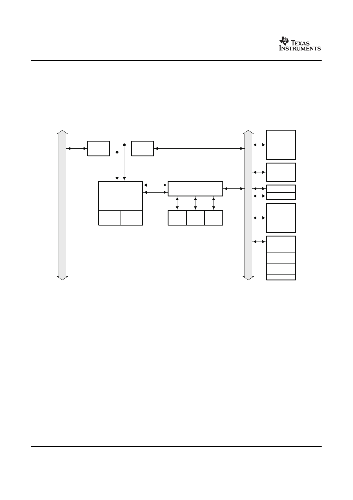
www.ti.com
PRODUCT PREVIEW
ARM926EJ-S
16KI$
8KD$ MMU
CP15
Arbiter Arbiter
I-AHB
D-AHB
Master
IF
DMAbus
I-TCM
D-TCM
16K
RAM0
RAM1
16K
ROM
8K
Arbiter
Slave
IF
MasterIF
CFGbus
ARM
interrupt
controller
(AINTC)
control
System
PLLC2
PLLC1
(PSC)
controller
sleep
Power
Peripherals
...
3.2 ARM926EJ-S RISC CPU
TMS320DM355
Digital Media System-on-Chip (DMSoC)
SPRS463 – SEPTEMBER 2007
– Image Pipe (IPIPE)
– H3A Engine (Hardware engine for computing Auto-focus, Auto white balance, and Auto exposure)
– Multiply Mask / Lens Distortion Module (CFALD)
• Video Processing Back End (VPBE)
– On Screen Display (OSD)
– Video Encoder Engine (VENC)
Figure 3-1 shows the functional block diagram of the DM355 ARM Subsystem.
Figure 3-1. DM355 ARM Subsystem Block Diagram
The ARM Subsystem integrates the ARM926EJ-S processor. The ARM926EJ-S processor is a member of
ARM9 family of general-purpose microprocessors. This processor is targeted at multi-tasking applications
where full memory management, high performance, low die size, and low power are all important. The
ARM926EJ-S processor supports the 32-bit ARM and 16 bit THUMB instruction sets, enabling the user to
trade off between high performance and high code density. Specifically, the ARM926EJ-S processor
supports the ARMv5TEJ instruction set, which includes features for efficient execution of Java byte codes,
providing Java performance similar to Just in Time (JIT) Java interpreter, but without associated code
overhead.
The ARM926EJ-S processor supports the ARM debug architecture and includes logic to assist in both
hardware and software debug. The ARM926EJ-S processor has a Harvard architecture and provides a
complete high performance subsystem, including:
• ARM926EJ -S integer core
• CP15 system control coprocessor
• Memory Management Unit (MMU)
• Separate instruction and data Caches
• Write buffer
• Separate instruction and data Tightly-Coupled Memories (TCMs) [internal RAM] interfaces
Detailed Device Description60 Submit Documentation Feedback
Page 61

www.ti.com
3.2.1 CP15
3.2.2 MMU
3.2.3 Caches and Write Buffer
TMS320DM355
Digital Media System-on-Chip (DMSoC)
SPRS463 – SEPTEMBER 2007
• Separate instruction and data AHB bus interfaces
• Embedded Trace Module and Embedded Trace Buffer (ETM/ETB)
For more complete details on the ARM9, refer to the ARM926EJ-S Technical Reference Manual, available
at http://www.arm.com
The ARM926EJ-S system control coprocessor (CP15) is used to configure and control instruction and
data caches, Tightly-Coupled Memories (TCMs), Memory Management Unit (MMU), and other ARM
subsystem functions. The CP15 registers are programmed using the MRC and MCR ARM instructions,
when the ARM in a privileged mode such as supervisor or system mode.
The ARM926EJ-S MMU provides virtual memory features required by operating systems such as Linux,
WindowCE, ultron, ThreadX, etc. A single set of two level page tables stored in main memory is used to
control the address translation, permission checks and memory region attributes for both data and
instruction accesses. The MMU uses a single unified Translation Lookaside Buffer (TLB) to cache the
information held in the page tables. The MMU features are:
• Standard ARM architecture v4 and v5 MMU mapping sizes, domains and access protection scheme.
• Mapping sizes are:
– 1MB (sections)
– 64KB (large pages)
– 4KB (small pages)
– 1KB (tiny pages)
• Access permissions for large pages and small pages can be specified separately for each quarter of
the page (subpage permissions)
• Hardware page table walks
• Invalidate entire TLB, using CP15 register 8
• Invalidate TLB entry, selected by MVA, using CP15 register 8
• Lockdown of TLB entries, using CP15 register 10
The size of the Instruction Cache is 16KB, Data cache is 8KB. Additionally, the Caches have the following
features:
• Virtual index, virtual tag, and addressed using the Modified Virtual Address (MVA)
• Four-way set associative, with a cache line length of eight words per line (32-bytes per line) and with
two dirty bits in the Dcache
• Dcache supports write-through and write-back (or copy back) cache operation, selected by memory
region using the C and B bits in the MMU translation tables.
• Critical-word first cache refilling
• Cache lockdown registers enable control over which cache ways are used for allocation on a line fill,
providing a mechanism for both lockdown, and controlling cache corruption
• Dcache stores the Physical Address TAG (PA TAG) corresponding to each Dcache entry in the TAG
RAM for use during the cache line write-backs, in addition to the Virtual Address TAG stored in the
TAG RAM. This means that the MMU is not involved in Dcache write-back operations, removing the
possibility of TLB misses related to the write-back address.
• Cache maintenance operations provide efficient invalidation of, the entire Dcache or Icache, regions of
the Dcache or Icache, and regions of virtual memory.
Submit Documentation Feedback Detailed Device Description 61
Page 62

www.ti.com
PRODUCT PREVIEW
3.2.4 Tightly Coupled Memory (TCM)
3.2.5 Advanced High-performance Bus (AHB)
3.2.6 Embedded Trace Macrocell (ETM) and Embedded Trace Buffer (ETB)
3.3 Memory Mapping
3.3.1 ARM Internal Memories
TMS320DM355
Digital Media System-on-Chip (DMSoC)
SPRS463 – SEPTEMBER 2007
The write buffer is used for all writes to a noncachable bufferable region, write-through region and write
misses to a write-back region. A separate buffer is incorporated in the Dcache for holding write-back for
cache line evictions or cleaning of dirty cache lines. The main write buffer has 16-word data buffer and a
four-address buffer. The Dcache write-back has eight data word entries and a single address entry.
ARM internal RAM is provided for storing real-time and performance-critical code/data and the Interrupt
Vector table. ARM internal ROM enables non-AEMIF boot options, such as NAND, UART, and HPI. The
RAM and ROM memories interfaced to the ARM926EJ-S via the tightly coupled memory interface that
provides for separate instruction and data bus connections. Since the ARM TCM does not allow
instructions on the D-TCM bus or data on the I-TCM bus, an arbiter is included so that both data and
instructions can be stored in the internal RAM/ROM. The arbiter also allows accesses to the RAM/ROM
from extra-ARM sources (e.g., EDMA or other masters). The ARM926EJ-S has built-in DMA support for
direct accesses to the ARM internal memory from a non-ARM master. Because of the time-critical nature
of the TCM link to the ARM internal memory, all accesses from non-ARM devices are treated as DMA
transfers.
Instruction and Data accesses are differentiated via accessing different memory map regions, with the
instruction region from 0x0000 through 0x7FFF and data from 0x10000 through 0x17FFF. Placing the
instruction region at 0x0000 is necessary to allow the ARM Interrupt Vector table to be placed at 0x0000,
as required by the ARM architecture. The internal 32-KB RAM is split into two physical banks of 16KB
each, which allows simultaneous instruction and data accesses to be accomplished if the code and data
are in separate banks.
The ARM Subsystem uses the AHB port of the ARM926EJ-S to connect the ARM to the configuration bus
and the external memories. Arbiters are employed to arbitrate access to the separate D-AHB and I-AHB
by the configuration bus and the external memories bus.
To support real-time trace, the ARM926EJ-S processor provides an interface to enable connection of an
Embedded Trace Macrocell (ETM). The ARM926ES-J Subsystem in DM355 also includes the Embedded
Trace Buffer (ETB). The ETM consists of two parts:
• Trace Port provides real-time trace capability for the ARM9.
• Triggering facilities provide trigger resources, which include address and data comparators, counter,
and sequencers.
The DM355 trace port is not pinned out and is instead only connected to the Embedded Trace Buffer. The
ETB has a 4KB buffer memory. ETB enabled debug tools are required to read/interpret the captured trace
data.
The ARM memory map is shown in Table 2-2 and Table 2-3 . This section describes the memories and
interfaces within the ARM's memory map.
The ARM has access to the following ARM internal memories:
• 32KB ARM Internal RAM on TCM interface, logically separated into two 16KB pages to allow
simultaneous access on any given cycle if there are separate accesses for code (I-TCM bus) and data
(D-TCM) to the different memory regions.
• 8KB ARM Internal ROM
Detailed Device Description62 Submit Documentation Feedback
Page 63
www.ti.com
3.3.2 External Memories
3.3.3 Peripherals
3.4 ARM Interrupt Controller (AINTC)
3.4.1 Interrupt Mapping
TMS320DM355
Digital Media System-on-Chip (DMSoC)
SPRS463 – SEPTEMBER 2007
The ARM has access to the following External memories:
• DDR2 / mDDR Synchronous DRAM
• Asynchronous EMIF / OneNAND
• NAND Flash
• Flash card devices:
– MMC/SD
– xD
– SmartMedia
The ARM has access to all of the peripherals on the device.
The DM355 ARM Interrupt Controller (AINTC) has the following features:
• Supports up to 64 interrupt channels (16 external channels)
• Interrupt mask for each channel
• Each interrupt channel can be mapped to a Fast Interrupt Request (FIQ) or to an Interrupt Request
(IRQ) type of interrupt.
• Hardware prioritization of simultaneous interrupts
• Configurable interrupt priority (2 levels of FIQ and 6 levels of IRQ)
• Configurable interrupt entry table (FIQ and IRQ priority table entry) to reduce interrupt processing time
The ARM core supports two interrupt types: FIQ and IRQ. See the ARM926EJ-S Technical Reference
Manual for detailed information about the ARM’s FIQ and IRQ interrupts. Each interrupt channel is
mappable to an FIQ or to an IRQ type of interrupt, and each channel can be enabled or disabled. The
INTC supports user-configurable interrupt-priority and interrupt entry addresses. Entry addresses minimize
the time spent jumping to interrupt service routines (ISRs). When an interrupt occurs, the corresponding
highest priority ISR’s address is stored in the INTC’s ENTRY register. The IRQ or FIQ interrupt routine can
read the ENTRY register and jump to the corresponding ISR directly. Thus, the ARM does not require a
software dispatcher to determine the asserted interrupt.
The AINTC takes up to 64 ARM device interrupts and maps them to either the IRQ or to the FIQ of the
ARM. Each interrupt is also assigned one of 8 priority levels (2 for FIQ, 6 for IRQ). For interrupts with the
same priority level, the priority is determined by the hardware interrupt number (the lowest number has the
highest priority). Table 3-1 shows the connection of device interrupts to the ARM.
Table 3-1. AINTC Interrupt Connections
(1)
Interrupt Acronym Source Interrupt Acronym Source
Number Number
0 VPSSINT0 VPSS - INT0, 32 TINT0 Timer 0 - TINT12
Configurable via
VPSSBL register:
INTSEL
1 VPSSINT1 VPSS - INT1 33 TINT1 Timer 0 - TINT34
2 VPSSINT2 VPSS - INT2 34 TINT2 Timer 1 - TINT12
3 VPSSINT3 VPSS - INT3 35 TINT3 Timer 1 - TINT34
4 VPSSINT4 VPSS - INT4 36 PWMINT0 PWM0
(1) The total number of interrupts in DM355 exceeds 64, which is the maximum value of the AINTC module. Therefore, several interrupts
are multiplexed and you must use the register ARM_INTMUX in the System Control Module to select the interrupt source for multiplexed
interrupts. Refer to the ARM Subsystem Guide for more information on the System Control Module register ARM_INTMUX.
Submit Documentation Feedback Detailed Device Description 63
Page 64

www.ti.com
PRODUCT PREVIEW
TMS320DM355
Digital Media System-on-Chip (DMSoC)
SPRS463 – SEPTEMBER 2007
Table 3-1. AINTC Interrupt Connections (continued)
Interrupt Acronym Source Interrupt Acronym Source
Number Number
5 VPSSINT5 VPSS - INT5 37 PWMINT1 PWM 1
6 VPSSINT6 VPSS - INT6 38 PWMINT2 PWM2
7 VPSSINT7 VPSS - INT7 39 I2CINT I2C
8 VPSSINT8 VPSS - INT8 40 UARTINT0 UART0
9 Reserved 41 UARTINT1 UART1
10 Reserved 42 SPINT0-0 SPI0
11 Reserved 43 SPINT0-1 SPI0
12 USBINT USB OTG Collector 44 GPIO0 GPIO
13 RTOINT or RTO or 45 GPIO1 GPIO
TINT4 Timer 2 - TINT12
SYS.ARM_INTMUX
14 UARTINT2 or UART2 or 46 GPIO2 GPIO
TINT5 Timer 2 - TINT34
15 TINT6 Timer 3 TINT12 47 GPIO3 GPIO
16 CCINT0 EDMA CC Region 0 48 GPIO4 GPIO
17 SPINT1-0 or SPI1 or 49 GPIO5 GPIO
CCERRINT EDMA CC Error
18 SPINT1-1 or SPI1 or 50 GPIO6 GPIO
TCERRINT0 EDMA TC0 Error
19 SPINT2-0 or SPI2 or 51 GPIO7 GPIO
TCERRINT1 EDMA TC1 Error
20 PSCINT PSC - ALLINT 52 GPIO8 GPIO
21 SPINT2-1 SPI2 53 GPIO9 GPIO
22 TINT7 Timer3 - TINT34 54 GPIOBNK0 GPIO
23 SDIOINT0 MMC/SD0 55 GPIOBNK1 GPIO
24 MBXINT0 or ASP0 or 56 GPIOBNK2 GPIO
MBXINT1 ASP1
25 MBRINT0 or ASP0 or 57 GPIOBNK3 GPIO
MBRINT1 ASP1
26 MMCINT0 MMC/SD0 58 GPIOBNK4 GPIO
27 MMCINT1 MMC/SC1 59 GPIOBNK5 GPIO
28 PWMINT3 PWM3 60 GPIOBNK6 GPIO
29 DDRINT DDR EMIF 61 COMMTX ARMSS
30 AEMIFINT Async EMIF 62 COMMRX ARMSS
31 SDIOINT1 SDIO1 63 EMUINT E2ICE
Detailed Device Description64 Submit Documentation Feedback
Page 65

www.ti.com
3.5 Device Clocking
3.5.1 Overview
TMS320DM355
Digital Media System-on-Chip (DMSoC)
SPRS463 – SEPTEMBER 2007
The DM355 requires one primary reference clock . The reference clock frequency may be generated
either by crystal input or by external oscillator. The reference clock is the clock at the pins named
MXI1/MXOI. The reference clock drives two separate PLL controllers (PLLC1 and PLLC2). PLLC1
generates the clocks required by the ARM, MPEG and JPEG co-processor, VPBE, VPSS, and
peripherals. PLL2 generates the clock required by the DDR PHY. A block diagram of DM355's clocking
architecture is shown in Figure 5-1 . The PLLs are described further in Section 3.6 .
Submit Documentation Feedback Detailed Device Description 65
Page 66

www.ti.com
PRODUCT PREVIEW
ARMsubsystem
MPEG/JPEG
co-Processor
SYSCLK1
SYSCLK2
VPFE
VPBE
DAC
DDRPHY
DDR
PLLDIV1(/1)
BPDIV(/8)
PLL controller2
PLL controller1
PLLDIV3(/n)
PLLDIV2(/4)
PLLDIV1(/2)
SYSCLK3
I2C
Timers(x4)
PWMs(x4)
SPI(x3)
MMC/SD(x2)
EMIF/NAND
ASP (x2)
GPIO
UART2
ARMINTC
USB
60MHz
Reference
clock
(MXI/MXO)
(24MHzor
36MHz)
Referenceclock
(MXI/MXO)
24MHzor36Mhz
PCLK
AUXCLK(/1)
BPDIV(/3)
SYSCLK1
CLKOUT3
SYSCLKBP
CLKOUT2
EDMA
Buslogic
Syslogic
PSC
IcePick
EXTCLK
RTO
USBPhy
SYSCLKBP
AUXCLK
PLLDIV4(/4or/2)
VPSS
UART0,1
CLKOUT1
Sequencer
SYSCLK4
3.5.2 Supported Clocking Configurations for DM355 - 216
TMS320DM355
Digital Media System-on-Chip (DMSoC)
SPRS463 – SEPTEMBER 2007
Figure 3-2. Device Clocking Block Diagram
This section describes the only supported device clocking configurations for DM355 - 216. The DM355
supports either 24 MHz (typical) or 36 MHz reference clock (crystal or external oscillator input).
Configurations are shown for both cases.
Detailed Device Description66 Submit Documentation Feedback
Page 67

www.ti.com
TMS320DM355
Digital Media System-on-Chip (DMSoC)
SPRS463 – SEPTEMBER 2007
3.5.2.1 Supported Clocking Configurations for DM355 - 216 (24 MHz reference)
3.5.2.1.1 DM355 - 216 PLL1 (24 MHz reference)
All supported clocking configurations for DM355 - 216 PLL1 with 24 MHz reference clock are shown in
Table 3-2
Table 3-2. PLL1 Supported Clocking Configurations for DM355 - 216 (24 MHz reference)
PREDI PLLM POSTDIV PLL1 ARM / Peripherals Venc VPSS
V VCO MPEG and
JPEG
Co-Processor
(/8 (m (/2 or /1 (MHz) PLLDIV SYSC PLLDIV SYSCLK2 PLLDIV3 SYSCL PLLDIV4 SYSCLK
fixed) programmable programma 1 LK1 2 (MHz) (/n K3 (/4 or /2 4
) ble) (/2 (MHz) (/4 programma (MHz) programmable (MHz)
fixed) fixed) ble) )
bypass bypass bypass bypas 2 12 4 6 10 2.4 4 6
s
8 144 1 432 2 216 4 108 16 27 4 108
8 135 1 405 2 202.5 4 101.25 15 27 4 101.25
8 126 1 378 2 189 4 94.5 14 27 4 94.5
8 117 1 351 2 175.5 4 87.75 13 27 4 87.75
8 108 1 324 2 162 4 81 12 27 4 81
8 99 1 297 2 148.5 4 74.25 11 27 4 74.25
8 180 2 270 2 135 4 67.5 10 27 2 135
8 162 2 243 2 121.5 4 60.75 9 27 2 121.5
8 144 2 216 2 108 4 54 8 27 2 108
8 126 2 189 2 94.5 4 47.25 7 27 2 94.5
8 108 2 162 2 81 4 40.5 6 27 2 81
3.5.2.1.2 DM355 - 216 PLL2 (24 MHz reference)
All supported clocking configurations for DM355 - 216 PLL2 with 24 MHz reference clock are shown in
Table 3-3
Table 3-3. PLL2 Supported Clocking Configurations for DM355 - 216 (24 MHz reference)
PREDIV PLLM POSTDIV PLL2 VCO DDR PHY DDR Clock
(/n programmable) (m (/2 fixed) (MHz) PLLDIV1 SYSCLK1 DDR_CLK
programmable) (/1 fixed) (MHz) (MHz)
bypass bypass bypass bypass 1 24 12
8 114 1 342 1 342 171
8 108 1 324 1 324 162
8 102 1 306 1 306 153
8 96 1 288 1 288 144
12 133 1 266 1 266 133
12 100 1 200 1 200 100
15 100 1 160 1 160 80
3.5.2.2 Supported Clocking Configurations for DM355 - 216 (36 MHz reference)
3.5.2.2.1 DM355 - 216 PLL1 (36 MHz reference)
All supported clocking configurations for DM355 - 216 PLL1 with 36 MHz reference clock are shown in
Table 3-4
Submit Documentation Feedback Detailed Device Description 67
Page 68

www.ti.com
PRODUCT PREVIEW
3.5.3 Supported Clocking Configurations for DM355 270
TMS320DM355
Digital Media System-on-Chip (DMSoC)
SPRS463 – SEPTEMBER 2007
Table 3-4. PLL1 Supported Clocking Configurations DM355 - 216 (36 MHz reference)
PREDI PLLM POSTDIV PLL1 ARM / Peripherals Venc VPSS
V VCO MPEG and
JPEG
Co-Processor
(/8 (m (/2 or /1 (MHz) PLLDIV SYSCL PLLDIV SYSCLK PLLDIV3 SYSCLK PLLDIV4 SYSCLK
fixed) programmable programma 1 K1 2 2 (/n 3 (/4 or /2 4
) ble) (/2 (MHz) (/4 (MHz) programma (MHz) programmable (MHz)
fixed) fixed) ble) )
bypass bypass bypass bypass 2 18 4 9 10 3.6 4 9
8 96 1 432 2 216 4 108 16 27 4 108
8 180 2 405 2 202.5 4 101.25 15 27 4 101.25
8 168 2 378 2 189 4 94.5 14 27 4 94.5
8 156 2 351 2 175.5 4 87.75 13 27 4 87.75
8 144 2 324 2 162 4 81 12 27 4 81
8 132 2 297 2 148.5 4 74.25 11 27 4 74.25
8 120 2 270 2 135 4 67.5 10 27 2 135
8 108 2 243 2 121.5 4 60.75 9 27 2 121.5
8 96 2 216 2 108 4 54 8 27 2 108
3.5.2.2.2 DM355 - 216 PLL2 (36 MHz reference)
All supported clocking configurations for DM355 - 216 PLL2 with 36 MHz reference clock are shown in
Table 3-5
Table 3-5. PLL2 Supported Clocking Configurations for DM355 - 216 (36 MHz reference)
PREDIV PLLM POSTDIV PLL2 VCO DDR PHY DDR Clock
(/n programmable) (m (/2 fixed) (MHz) PLLDIV1 SYSCLK1 DDR_CLK
programmable) (/1 fixed) (MHz) (MHz)
bypass bypass bypass bypass 1 36 18
12 114 1 342 1 342 171
12 108 1 324 1 324 162
12 102 1 306 1 306 153
12 96 1 288 1 288 144
18 133 1 266 1 266 133
27 150 1 200 1 200 100
27 120 1 160 1 160 80
This section describes the only supported device clocking configurations for DM355 - 270. The DM355
supports either 24 MHz (typical) or 36 MHz reference clock (crystal or external oscillator input).
Configurations are shown for both cases.
3.5.3.1 Supported Clocking Configurations for DM355 - 270 (24 MHz reference)
3.5.3.1.1 DM355 - 270 PLL1 (24 MHz reference)
All supported clocking configurations for DM355 - 270 PLL1 with 24 MHz reference clock are shown in
Table 3-2
Detailed Device Description68 Submit Documentation Feedback
Page 69

www.ti.com
TMS320DM355
Digital Media System-on-Chip (DMSoC)
SPRS463 – SEPTEMBER 2007
Table 3-6. PLL1 Supported Clocking Configurations for DM355 - 270 (24 MHz reference)
PRED PLLM POSTDIV PLL1 ARM / Peripherals Venc VPSS
IV VCO MPEG and JPEG
Co-Processor
(/8 (m (/2 fixed) (MHz) PLLDIV1 SYSC PLLDI SYSCLK2 PLLDIV3 SYSCLK PLLDIV4 SYSCLK4
fixed) programmable) (/2 fixed) LK1 V2 (MHz) (/n 3 (/2 fixed) (MHz)
(MHz) (/4 programmable) (MHz)
fixed)
bypas bypass bypass bypas 2 12 4 6 10 2.4 4 6
s s
8 180 1 540 2 270 4 135 20 27 4 135
8 171 1 513 2 256.5 4 128.25 19 27 4 128.25
8 162 1 486 2 243 4 121.5 18 27 4 121.5
8 153 1 459 2 229.5 4 114.75 17 27 4 114.75
8 144 1 432 2 216 4 108 16 27 4 108
8 135 1 405 2 202.5 4 101.25 15 27 4 101.25
8 126 1 378 2 189 4 94.5 14 27 4 94.5
8 117 1 351 2 175.5 4 87.75 13 27 4 87.75
8 108 1 324 2 162 4 81 12 27 4 81
8 99 1 297 2 148.5 4 74.25 11 27 4 74.25
8 180 2 270 2 135 4 67.5 10 27 2 135
8 162 2 243 2 121.5 4 60.75 9 27 2 121.5
8 144 2 216 2 108 4 54 8 27 2 108
8 126 2 189 2 94.5 4 47.25 7 27 2 94.5
8 108 2 162 2 81 4 40.5 6 27 2 81
3.5.3.1.2 DM355 - 270 PLL2 (24 MHz reference)
All supported clocking configurations for DM355 - 270 PLL2 with 24 MHz reference clock are shown in
Table 3-3
Table 3-7. PLL2 Supported Clocking Configurations for DM355 - 270 (24 MHz reference)
PREDIV PLLM POSTDIV PLL2 VCO DDR PHY DDR Clock
(/n programmable) (m (/2 fixed) (MHz) PLLDIV1 SYSCLK1 DDR_CLK
programmable) (/1 fixed) (MHz) (MHz)
bypass bypass bypass bypass 1 24 12
8 114 1 342 1 342 171
8 108 1 324 1 324 162
8 102 1 306 1 306 153
8 96 1 288 1 288 144
12 133 1 266 1 266 133
12 100 1 200 1 200 100
15 100 1 160 1 160 80
3.5.3.2 Supported Clocking Configurations for DM355 - 270 (36 MHz reference)
3.5.3.2.1 DM355 - 270 PLL1 (36 MHz reference)
All supported clocking configurations for DM355 - 270 PLL1 with 36 MHz reference clock are shown in
Table 3-4
Submit Documentation Feedback Detailed Device Description 69
Page 70

www.ti.com
PRODUCT PREVIEW
TMS320DM355
Digital Media System-on-Chip (DMSoC)
SPRS463 – SEPTEMBER 2007
Table 3-8. PLL1 Supported Clocking Configurations for DM355 - 270 (36 MHz reference)
PREDI PLLM POSTDI PLL1 ARM / Peripherals Venc VPSS
V V VCO MPEG and
JPEG
Co-Processor
(/8 (m (/2 fixed) (MHz) PLLDIV SYSC PLLDIV SYSCLK2 PLLDIV3 SYSCL PLLDIV4 SYSCLK4
fixed) programmable) 1 LK1 2 (MHz) (/n K3 (/2 fixed) (MHz)
(/2 (MHz) (/4 programmable) (MHz)
fixed) fixed)
bypas bypass bypass bypas 2 18 4 9 10 3.6 4 18
s s
8 120 1 540 2 270 4 135 20 27 4 135
8 114 1 513 2 256.5 4 128.25 19 27 4 128.25
8 108 1 486 2 243 4 121.5 18 27 4 121.5
8 102 1 459 2 229.5 4 114.75 17 27 4 114.75
8 96 2 432 2 216 4 108 16 27 4 108
8 180 2 405 2 202.5 4 101.25 15 27 2 202.5
8 168 2 378 2 189 4 94.5 14 27 2 189
8 156 2 351 2 175.5 4 87.75 13 27 2 175.5
8 144 2 324 2 162 4 81 12 27 2 162
8 132 2 297 2 148.5 4 74.25 11 27 2 148.5
8 120 2 270 2 135 4 67.5 10 27 2 135
8 108 2 243 2 121.5 4 60.75 9 27 2 121.5
8 96 2 216 2 108 4 54 8 27 2 108
Detailed Device Description70 Submit Documentation Feedback
Page 71

www.ti.com
3.5.4 Peripheral Clocking Considerations
TMS320DM355
Digital Media System-on-Chip (DMSoC)
SPRS463 – SEPTEMBER 2007
3.5.3.2.2 DM355 - 270 PLL2 (36 MHz reference)
All supported clocking configurations for DM355 - 270 PLL2 with 36 MHz reference clock are shown in
Table 3-5
Table 3-9. PLL2 Supported Clocking Configurations for DM355L (36 MHz reference)
PREDIV PLLM POSTDIV PLL2 VCO DDR PHY DDR Clock
(/n programmable) (m (/2 fixed) (MHz) PLLDIV1 SYSCLK1 DDR_CLK
programmable) (/1 fixed) (MHz) (MHz)
bypass bypass bypass bypass 1 36 18
12 114 1 342 1 342 171
12 108 1 324 1 324 162
12 102 1 306 1 306 153
12 96 1 288 1 288 144
18 133 1 266 1 266 133
27 150 1 200 1 200 100
27 120 1 160 1 160 80
3.5.4.1 Video Processing Back End Clocking
The Video Processing Back End (VPBE) is a sub-module of the VPSS (Video Processing Subsystem).
The VPBE is designed to interface with a variety of LCDs and an internal DAC module. There are two
asynchronous clock domains in the VPBE: an internal clock domain and an external clock domain. The
internal clock domain is driven by the VPSS clock (PLL1 SYSCLK4). The external clock domain is
configurable; you can select one of five source:
• 24 MHz crystal input at MXI1
• 27 MHz crystal input at MXI2 (optional feature, not typically used)
• PLL1 SYSCLK3
• EXTCLK pin (external VPBE clock input pin)
• PCLK pin (VPFE pixel clock input pin)
See the TMS320DM355 DMSoC Video Processing Back End (VPBE) User's Guide for complete
information on VPBE clocking.
3.5.4.2 USB Clocking
The USB Controller is driven by two clocks: an output clock of PLL1 (SYSCLK2) and an output clock of
the USB PHY.
NOTE
For proper USB function, SYSCLK2 must be greater than 60 MHz.
The USB PHY takes an input clock that is configurable by the USB PHY clock source bits (PHYCLKSRC)
in the USB PHY control register (USB_PHY_CTL) in the System Control Module. When a 24 MHz crystal
is used at MXI1/MXO1, set PHYCLKSRC to 0. This will present a 24 MHz clock to the USB PHY. When a
36 MHz crystal is used at MXI1/MXO1, set PHYCLKSRC to 1. This will present a 12 MHz clock (36 MHz
divided internally by three) to the USB PHY. The USB PHY is capable of accepting only 24 MHz and 12
MHz; thus you must use either a 24 MHz or 36 MHz crystal at MXI1/MXO1. See the TMS320DM355
DMSoC Univeral Serial Bus (USB) Controller User's Guide (SPRUED2) for more information. See the
TMS320DM355 DMSoC ARM Subsystem User's Guide for more information on the System Control
Module.
Submit Documentation Feedback Detailed Device Description 71
Page 72

www.ti.com
PRODUCT PREVIEW
3.6 PLL Controller (PLLC)
3.6.1 PLL Controller Module
TMS320DM355
Digital Media System-on-Chip (DMSoC)
SPRS463 – SEPTEMBER 2007
This section describes the PLL Controllers for PLL1 and PLL2. See the TMS320DM355 Digital Media
System-on-Chip ARM Subsystem User's Guide for more information on the PLL controllers.
The DM355 has two PLL controllers that provide clocks to different components of the chip. PLL controller
1 (PLLC1) provides clocks to most of the components of the chip. PLL controller 2 (PLLC2) provides
clocks to the DDR PHY.
As a module, the PLL controller provides the following:
• Glitch-free transitions (on changing PLL settings)
• Domain clocks alignment
• Clock gating
• PLL bypass
• PLL power down
The various clock outputs given by the PLL controller are as follows:
• Domain clocks: SYSCLKn
• Bypass domain clock: SYSCLKBP
• Auxiliary clock from reference clock: AUXCLK
Various dividers that can be used are as follows:
• Pre-PLL divider: PREDIV
• Post-PLL divider: POSTDIV
• SYSCLK divider: PLLDIV1, … , PLLDIVn
• SYSCLKBP divider: BPDIV
Multipliers supported are as follows:
• PLL multiplier control: PLLM
Detailed Device Description72 Submit Documentation Feedback
Page 73

www.ti.com
3.6.2 PLLC1
TMS320DM355
Digital Media System-on-Chip (DMSoC)
SPRS463 – SEPTEMBER 2007
PLLC1 provides most of the DM355 clocks. Software controls PLLC1 operation through the PLLC1
registers. The following list, Table 3-10 , and Figure 3-3 describe the customizations of PLLC1 in the
DM355.
• Provides primary DM355 system clock
• Software configurable
• Accepts clock input or internal oscillator input
• PLL pre-divider value is fixed to (/8)
• PLL multiplier value is programmable
• PLL post-divider
• Only SYSCLK[4:1] are used
• SYSCLK1 divider value is fixed to (/2)
• SYSCLK2 divider value is fixed to (/4)
• SYSCLK3 divider value is programmable
• SYSCLK4 divider value is programmable to (/4) or (/2)
• SYSCLKBP divider value is fixed to (/3)
• SYSCLK1 is routed to the ARM Subsystem
• SYSCLK2 is routed to peripherals
• SYSCLK3 is routed to the VPBE module
• SYSCLK4 is routed to the VPSS module
• AUXCLK is routed to peripherals with fixed clock domain and also to the output pin CLKOUT1
• SYSCLKBP is routed to the output pin CLKOUT2
Table 3-10. PLLC1 Output Clocks
Output Clock Used By PLLDIV Notes
Divider
SYSCLK1 ARM Subsystem / MPEG and JPEG Co-Processor /2 Fixed divider
SYSCLK2 Peripherals /4 Fixed divider
SYSCLK3 VPBE (VENC module) /n Programmable divider (used to get 27
MHz for VENC)
SYSCLK4 VPSS /4 or /2 Programmable divider
AUXCLK Peripherals, CLKOUT1 none No divider
SYSCLKBP CLKOUT2 /3 Fixed divider
Submit Documentation Feedback Detailed Device Description 73
Page 74
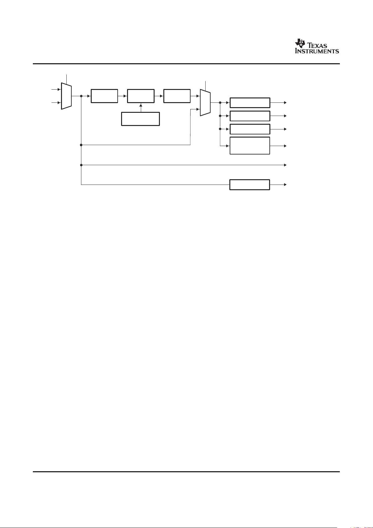
www.ti.com
PRODUCT PREVIEW
PLLDIV1(/2)
PLLDIV2(/4)
PLLDIV3(/3)
SYSCLK1
(ARMandMPEG/JPEG
Co-processor)
SYSCLK2
(peripherals)
SYSCLK3
(VPBE)
1
0
PLL
0
1
CLKMODE
CLKIN
OSCIN
PLLEN
AUXCLK
(Peripherals,
CLKOUT1)
SYSCLKBP
(CLKOUT2)
Pre-DIV
(/8)
Post-DIV
(/2or/1)
PLLM
(programmable)
BPDIV(/3)
PLLDIV4
(/4or/2)
SYSCLK4
(VPSS)
TMS320DM355
Digital Media System-on-Chip (DMSoC)
SPRS463 – SEPTEMBER 2007
Figure 3-3. PLLC1 Configuration In DM355
74 Detailed Device Description Submit Documentation Feedback
Page 75

www.ti.com
3.6.3 PLLC2
PLLDIV1(/1)
1
0
PLL
0
1
CLKMODE
CLKIN
OSCIN
PLLEN
SYSCLK1
(DDRPHY)
SYSCLKBP
(CLKOUT3)
BPDIV(/8)
PLLM
(programmable)
Pre-DIV
(programmable)
Post-DIV
(/1)
TMS320DM355
Digital Media System-on-Chip (DMSoC)
SPRS463 – SEPTEMBER 2007
PLLC2 provides the DDR PHY clock and CLKOUT3. Software controls PLLC2 operation through the
PLLC2 registers. The following list, Table 3-11 , and Figure 3-4 describe the customizations of PLLC2 in
the DM355.
• Provides DDR PHY clock and CLKOUT3
• Software configurable
• Accepts clock input or internal oscillator input (same input as PLLC1)
• PLL pre-divider value is programmable
• PLL multiplier value is programmable
• PLL post-divider value is fixed to (/1)
• Only SYSCLK[1] is used
• SYSCLK1 divider value is fixed to (/1)
• SYSCLKBP divider value is fixed to (/8)
• SYSCLK1 is routed to the DDR PHY
• SYSCLKBP is routed to the output pin CLKOUT3
• AUXCLK is not used.
Table 3-11. PLLC2 Output Clocks
Output Clock Used by PLLDIV Divider Notes
SYSCLK1 DDR PHY /1 Fixed divider
SYSCLKBP CLKOUT3 /8 Fixed divider
PLLC2 Configuration in DM355
Submit Documentation Feedback Detailed Device Description 75
Page 76
www.ti.com
PRODUCT PREVIEW
3.7 Power and Sleep Controller (PSC)
arm_clock
arm_mreset
arm_power
AINTC
ARM
module_power
module_mreset
MODx
module_clock
Alwayson
domain
Interrupt
PSC
clks
PLLC
Emulation
RESETN
VDD
DMSoC
3.8 System Control Module
TMS320DM355
Digital Media System-on-Chip (DMSoC)
SPRS463 – SEPTEMBER 2007
In the DM355 system, the Power and Sleep Controller (PSC) is responsible for managing transitions of
system power on/off, clock on/off, and reset. A block diagram of the PSC is shown in Figure 3-5 . Many of
the operations of the PSC are transparent to software, such as power-on-reset operations. However, the
PSC provides you with an interface to control several important clock and reset operations.
The PSC includes the following features:
• Manages chip power-on/off, clock on/off, and resets
• Provides a software interface to:
– Control module clock ON/OFF
– Control module resets
• Supports IcePick emulation features: power, clock, and reset
For more information on the PSC, see the ARM Subsystem User's Guide.
Figure 3-5. DM355 Power and Sleep Controller (PSC)
The DM355’s system control module is a system-level module containing status and top-level control logic
required by the device. The system control module consists of a miscellaneous set of status and control
registers, accessible by the ARM and supporting all of the following system features and operations:
• Device identification
• Device configuration
– Pin multiplexing control
– Device boot configuration status
• ARM interrupt and EDMA event multiplexing control
• Special peripheral status and control
– Timer64+
– USB PHY control
– VPSS clock and video DAC control and status
– DDR VTP control
– Clockout circuitry
– GIO de-bounce control
Detailed Device Description76 Submit Documentation Feedback
Page 77
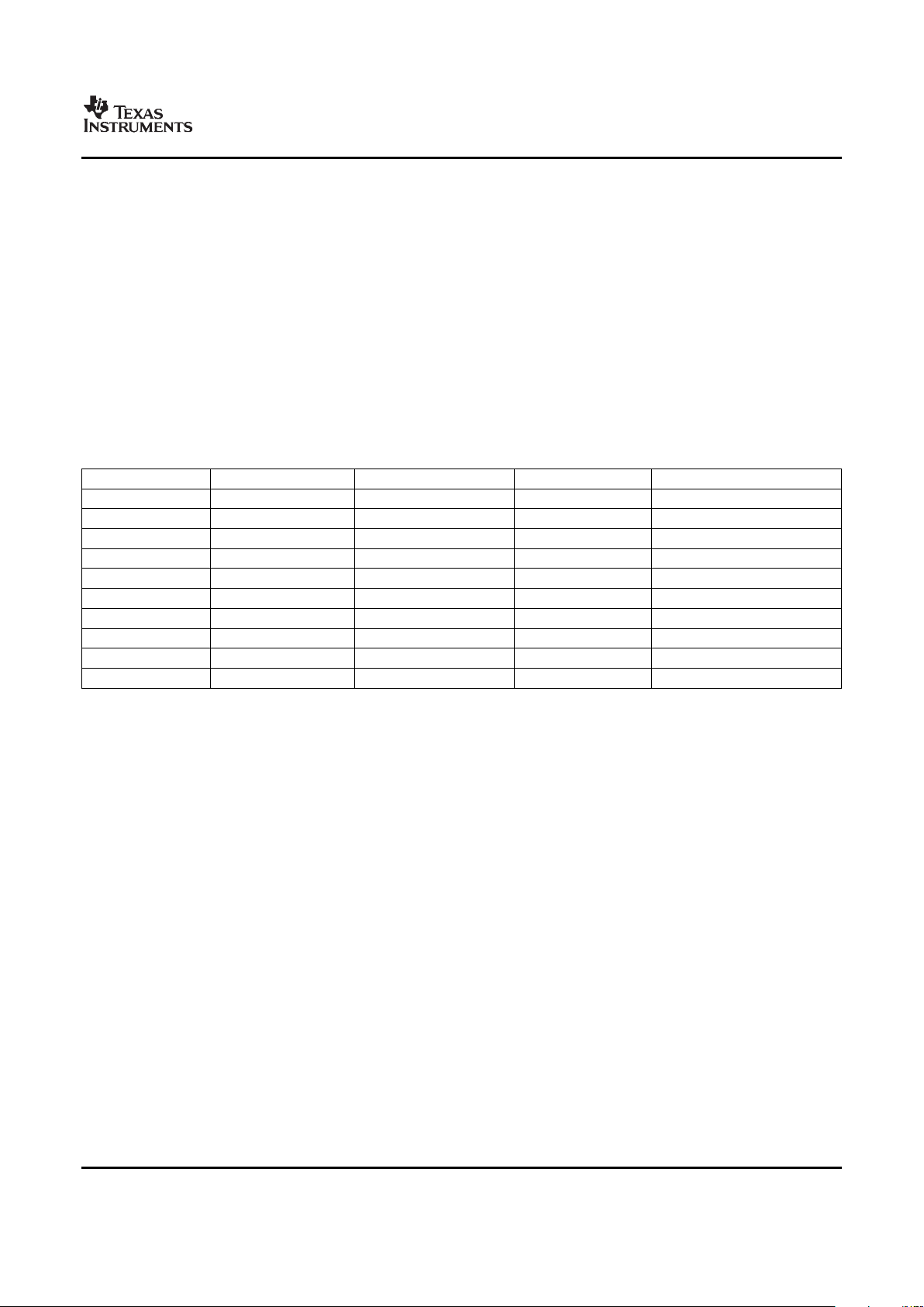
www.ti.com
3.9 Pin Multiplexing
3.9.1 Hardware Controlled Pin Multiplexing
TMS320DM355
Digital Media System-on-Chip (DMSoC)
SPRS463 – SEPTEMBER 2007
• Power management
– Deep sleep and fast NAND boot control
• Bandwidth Management
– Bus master DMA priority control
For more information on the System Control Module refer to the ARM Subsystem User's Guide.
The DM355 makes extensive use of pin multiplexing to accommodate the large number of peripheral
functions in the smallest possible package. In order to accomplish this, pin multiplexing is controlled using
a combination of hardware configuration (at device reset) and software control. No attempt is made by the
DM355 hardware to ensure that the proper pin muxing has been selected for the peripherals or interface
mode being used, thus proper pin muxing configuration is the responsibility of the board and software
designers. An overview of the pin multiplexing is shown in Table 3-12 .
Table 3-12. Peripheral Pin Mux Overview
Peripheral Muxed With Primary Function Secondary Function Tertiary Function
VPFE (video in) GPIO and SPI2 VPFE (video in) SPI2 GPIO
VPBE (video out) GPIO, PWM, and RTO VPBE (video out) PWM and RTO GPIO
AEMIF GPIO AEMIF GPIO none
ASP0 GPIO ASP0 GPIO none
MMC/SD1 GPIO and UART2 MMC/SD1 GPIO UART2
CLKOUT GPIO CLKOUT GPIO none
I2C GPIO I2C GPIO none
UART1 GPIO UART1 GPIO none
SPI1 GPIO SPI1 GPIO none
SPI0 GPIO SPI0 GPIO none
Use the Asynchronous EMIF configuration pins (AECFG[3:0]) for hardware pin mux control. AECFG[3:0]
control the partitioning of the AEMIF addresses and GPIOs at reset, which allows you to properly
configure the number of AEMIF address pins required by the boot device while unused addresses pins are
available as GPIOs. These settings may be changed by software after reset by programming the PinMux2
register The PinMux2 register is in the System Control Module. As shown in Table 3-13 , the number of
address bits enabled on the AEMIF is selectable from 0 to 16. Pins that are not assigned to another
peripheral and not enabled as address signals become GPIOs (except EM_A[2:1]). The enabled address
signals are always contiguous from EM_BA[1] upwards; bits cannot be skipped. The exception to this are
EM_A[2:1]. These signals (can be used to) represent the ALE and CLE signals for the NAND Flash mode
of the AEMIF and are always enabled. Note that EM_A[0] does not represent the lowest AEMIF address
bit. DM355 supports only 16-bit and 8-bit data widths for the AEMIF. In 16-bit mode, EM_BA[1] represents
the LS address bit (the half-word address) and EM_BA[0] represents the MS address bit (A[14]). In 8-bit
mode, EM_BA[1:0] represent the 2 LS address bits. Note that additional selections are available by
programming the PinMux2 register in software after boot. Note that AECFG selection of ‘0010’ selects
OneNAND interface. The AEMIF needs to operate in the half-rate mode (full_rate = 0) to meet frequency
requirements. Software should not change the PINMUX2 register setting to affect the AEMIF rate
operation. A soft reset of the AEMIF should be performed any time a rate change is made.
Submit Documentation Feedback Detailed Device Description 77
Page 78
www.ti.com
PRODUCT PREVIEW
3.9.2 Software Controlled Pin Multiplexing
3.10 Device Reset
TMS320DM355
Digital Media System-on-Chip (DMSoC)
SPRS463 – SEPTEMBER 2007
Table 3-13. AECFG (Async EMIF Configuration) Pin Mux Coding
1101(NAND) 1100 1010 (OneNAND) 1000 (8-bit SRAM) 0010 (16-bit SRAM) 0000
GPIO[54] GPIO[54] EM_A[14] EM_BA[0] EM_A[14] EM_BA[0]
GPIO[55] EM_BA[1] EM_BA[1] EM_BA[1] EM_BA[1] EM_BA[1]
GPIO[56] EM_A[0] EM_A[0] EM_A[0] EM_A[0] EM_A[0]
EM_A[1] EM_A[1] EM_A[1] EM_A[1] EM_A[1] EM_A[1]
EM_A[2] EM_A[2] EM_A[2] EM_A[2] EM_A[2] EM_A[2]
GPIO[57] EM_A[3] EM_A[3] EM_A[3] EM_A[3] EM_A[3]
GPIO[58] EM_A[4] EM_A[4] EM_A[4] EM_A[4] EM_A[4]
GPIO[59] EM_A[5] EM_A[5] EM_A[5] EM_A[5] EM_A[5]
GPIO[60] EM_A[6] EM_A[6] EM_A[6] EM_A[6] EM_A[6]
GPIO[61] EM_A[7] EM_A[7] EM_A[7] EM_A[7] EM_A[7]
GPIO[62] EM_A[8] EM_A[8] EM_A[8] EM_A[8] EM_A[8]
GPIO[63] EM_A[9] EM_A[9] EM_A[9] EM_A[9] EM_A[9]
GPIO[64] EM_A[10] EM_A[10] EM_A[10] EM_A[10] EM_A[10]
GPIO[65] EM_A[11] EM_A[11] EM_A[11] EM_A[11] EM_A[11]
GPIO[66] EM_A[12] EM_A[12] EM_A[12] EM_A[12] EM_A[12]
GPIO[67] EM_A[13] EM_A[13] EM_A[13] EM_A[13] EM_A[13]
GPIO[46] GPIO[46] GPIO[46] GPIO[46] EM_D[8] EM_D[8]
GPIO[47] GPIO[47] GPIO[47] GPIO[47] EM_D[9] EM_D[9]
GPIO[48] GPIO[48] GPIO[48] GPIO[48] EM_D[10] EM_D[10]
GPIO[49] GPIO[49] GPIO[49] GPIO[49] EM_D[11] EM_D[11]
GPIO[50] GPIO[50] GPIO[50] GPIO[50] EM_D[12] EM_D[12]
GPIO[51] GPIO[51] GPIO[51] GPIO[51] EM_D[13] EM_D[13]
GPIO[52] GPIO[52] GPIO[52] GPIO[52] EM_D[14] EM_D[14]
GPIO[53] GPIO[53] GPIO[53] GPIO[53] EM_D[15] EM_D[15]
All pin multiplexing options are configurable by software via pin mux registers that reside in the System
Control Module. The PinMux0 Register controls the Video In muxing, PinMux1 register controls Video Out
signals, PinMux2 register controls AEMIF signals, PinMux3 registers control the multiplexing of the GIO
signals, the PinMux4 register controls the SPI and MMC/SD0 signals. Refer to the ARM Subsystem User's
Guide for complete descriptions of the pin mux registers.
There are five types of reset in DM355. The types of reset differ by how they are initiated and/or by their
effect on the chip. Each type is briefly described in Table 3-14 and further described in the ARM
Subsystem Guide.
Table 3-14. Reset Types
Type Initiator Effect
POR (Power-On-Reset) RESET pin low and TRST low Total reset of the chip (cold reset). Resets all modules
including memory and emulation.
Warm Reset RESET pin low and TRST high (initiated by ARM Resets all modules including memory, except ARM
emulator). emulation.
Max Reset ARM emulator or Watchdog Timer (WDT). Same effect as warm reset.
System Reset ARM emulator Resets all modules except memory and ARM
emulation. It is a soft reset that maintains memory
contents and does not affect or reset clocks or power
states.
Detailed Device Description78 Submit Documentation Feedback
Page 79

www.ti.com
3.11 Default Device Configurations
3.11.1 Device Configuration Pins
TMS320DM355
Digital Media System-on-Chip (DMSoC)
SPRS463 – SEPTEMBER 2007
Table 3-14. Reset Types (continued)
Type Initiator Effect
Module Reset ARM software Resets a specific module. Allows the ARM to
independently reset any module. Module reset is
intended as a debug tool not as a tool to use in
production.
After POR, warm reset, and max reset, the chip is in its default configuration. This section highlights the
default configurations associated with PLLs, clocks, ARM boot mode, and AEMIF.
NOTE
Default configuration is the configuration immediately after POR, warm reset, and max
reset and just before the boot process begins. The boot ROM updates the configuration.
See Section 3.12 for more information on the boot process.
The device configuration pins are described in Table 3-15 . The device configuration pins are latched at
reset and allow you to configure all of the following options at reset:
• ARM Boot Mode
• Asynchronous EMIF pin configuration
These pins are described further in the following sections.
NOTE
The device configuration pins are multiplexed with AEMIF pins. After the device
configuration pins are sampled at reset, they automatically change to function as AEMIF
pins. Pin multiplexing is described in Section 3.8 .
Table 3-15. Device Configuration
Default Setting (by
internal
Device Sampled pull-up/
Configuration Input Function Pin pull-down) Device Configuration Affected
BTSEL[1:0] Selects ARM boot mode EM_A[13:12] 00 If any ROM boot mode is selected, GIO61
00 = Boot from ROM (NAND) (NAND) is used to indicated boot status.
01 = Boot from AEMIF If NAND boot is selected, CE0 is used for
10 = Boot from ROM NAND. Use AECFG[3:0] to configure
(MMC/SD) AEMIF pins for NAND.
11 = Boot from ROM (UART) If AEMIF boot is selected, CE0 is used for
AEMIF device (OneNAND, ROM). Use
AECFG[3:0] to configure AEMIF pins for
NAND.
If MMC/SD boot is selected, MMC/SD0 is
used.
AECFG[3:0] Selects AEMIF pin EM_A[11:8] 1101 Selects the AEMIF pin configuration. Refer
configuration (NAND) to pin-muxing information in Section 3.9.1 .
Note that AECFG[3:0] affects both AEMIF
(BTSEL[1:0]=01) and NAND
(BTSEL[1:0]=00) boot modes.
Submit Documentation Feedback Detailed Device Description 79
Page 80

www.ti.com
PRODUCT PREVIEW
3.11.2 PLL Configuration
3.11.3 Power Domain and Module State Configuration
TMS320DM355
Digital Media System-on-Chip (DMSoC)
SPRS463 – SEPTEMBER 2007
After POR, warm reset, and max reset, the PLLs and clocks are set to their default configurations. The
PLLs are in bypass mode and disabled by default. This means that the input reference clock at MXI1
(typically 24 MHz) drives the chip after reset. For more information on device clocking, see Section 3.5
and Section 3.6 . The default state of the PLLs is reflected in the default state of the register bits in the
PLLC registers. Refer the the ARM Subsystem User's Guide for PLLC register descriptions.
Only a subset of modules are enabled after reset by default. Table 3-16 shows which modules are
enabled after reset. Table 3-16 as shows that the following modules are enabled depending on the
sampled state of the device configuration pins: EDMA (CC and TC0), AEMIF, MMC/SD0, UART0, and
Timer0. For example, UART0 is enabled after reset when the device configuration pins (BTSEL[1:0] = 11 Enable UART) select UART boot mode. For more information on module configuration refer to the ARM
Subsystem User's Guide.
80 Detailed Device Description Submit Documentation Feedback
Page 81

www.ti.com
TMS320DM355
Digital Media System-on-Chip (DMSoC)
SPRS463 – SEPTEMBER 2007
Table 3-16. Module Configuration
Default States
Module Module Name Power Domain Power Domain State Module State
Number
0 VPSS Master AlwaysOn ON SyncRst
1 VPSS Slave AlwaysOn ON SyncRst
2 EDMA (CC) AlwaysOn ON BTSEL[1:0] = 00 – Enable (NAND)
BTSEL[1:0] = 01 – Enable (OneNAND)
3 EDMA (TC0) AlwaysOn ON BTSEL[1:0] = 10 – SyncRst (MMC/SD)
BTSEL[1:0] = 11 – Enable (UART)
4 EDMA (TC1) AlwaysOn ON SyncRst
5 Timer3 AlwaysOn ON SyncRst
6 SPI1 AlwaysOn ON SyncRst
7 MMC/SD1 AlwaysOn ON SyncRst
8 ASP1 AlwaysOn ON SyncRst
9 USB AlwaysOn ON SyncRst
10 PWM3 AlwaysOn ON SyncRst
11 SPI2 AlwaysOn ON SyncRst
12 RTO AlwaysOn ON SyncRst
13 DDR EMIF AlwaysOn ON SyncRst
14 AEMIF AlwaysOn ON BTSEL[1:0] = 00 – Enable (NAND)
BTSEL[1:0] = 01 – Enable (OneNAND)
BTSEL[1:0] = 10 – SyncRst (MMC/SD)
BTSEL[1:0] = 11 – Enable (UART)
15 MMC/SD0 AlwaysOn ON BTSEL[1:0] = 00 – Enable (NAND)
BTSEL[1:0] = 01 – Enable (OneNAND)
BTSEL[1:0] = 10 – SyncRst (MMC/SD)
BTSEL[1:0] = 11 – Enable (UART)
16 Reserved
17 ASP AlwaysOn ON SyncRst
18 I2C AlwaysOn ON SyncRst
19 UART0 AlwaysOn ON BTSEL[1:0] = 00 – Enable (NAND)
BTSEL[1:0] = 01 – Enable (OneNAND)
BTSEL[1:0] = 10 – SyncRst (MMC/SD)
BTSEL[1:0] = 11 – Enable (UART)
20 UART1 AlwaysOn ON SyncRst
21 UART2 AlwaysOn ON SyncRst
22 SPI0 AlwaysOn ON SyncRst
23 PWM0 AlwaysOn ON SyncRst
24 PWM1 AlwaysOn ON SyncRst
25 PWM2 AlwaysOn ON SyncRst
26 GPIO AlwaysOn ON SyncRst
27 TIMER0 AlwaysOn ON BTSEL[1:0] = 00 – Enable (NAND)
BTSEL[1:0] = 01 – Enable (OneNAND)
BTSEL[1:0] = 10 – SyncRst (MMC/SD)
BTSEL[1:0] = 11 – Enable (UART)
28 TIMER1 AlwaysOn ON SyncRst
29 TIMER2 AlwaysOn ON Enable
30 System Module AlwaysOn ON Enable
Submit Documentation Feedback Detailed Device Description 81
Page 82

www.ti.com
PRODUCT PREVIEW
3.11.4 ARM Boot Mode Configuration
3.11.5 AEMIF Configuration
3.12 Device Boot Modes
TMS320DM355
Digital Media System-on-Chip (DMSoC)
SPRS463 – SEPTEMBER 2007
Table 3-16. Module Configuration (continued)
Default States
31 ARM AlwaysOn ON Enable
32 BUS AlwaysOn ON Enable
33 BUS AlwaysOn ON Enable
34 BUS AlwaysOn ON Enable
35 BUS AlwaysOn ON Enable
36 BUS AlwaysOn ON Enable
37 BUS AlwaysOn ON Enable
38 BUS AlwaysOn ON Enable
39 Reserved Reserved Reserved Reserved
40 VPSS DAC Always On ON SyncRst
The input pins BTSEL[1:0] determine whether the ARM will boot from its ROM or from the Asynchronous
EMIF (AEMIF). When ROM boot is selected (BTSEL[1:0] = 00, 10, or 11), a jump to the start of internal
ROM (address 0x0000: 8000) is forced into the first fetched instruction word. The embedded ROM boot
loader code (RBL) then performs certain configuration steps, reads the BOOTCFG register to determine
the desired boot method, and branches to the appropriate boot routine (i.e., a NAND, MMC/SD, or UART
loader routine).
If AEMIF boot is selected (BTSEL[1:0] = 01), a jump to the start of AEMIF (address 0x0200: 0000) is
forced into the first fetched instruction word. The ARM then continues executing from external
asynchronous memory using the default AEMIF timings until modified by software.
NOTE
For AEMIF boot, the OneNAND must be connected to the first AEMIF chip select space
(EM_CE0). Also, the AEMIF does not support direct execution from NAND Flash.
Boot modes are further described in Section 3.12 .
3.11.5.1 AEMIF Pin Configuration
The input pins AECFG[3:0] determine the AEMIF configuration immediately after reset. Use AECFG[3:0]
to properly configure the pins of the AEMIF. Refer to the section on pin multiplexing in Section 3.9 .
Also, see the Asynchronous External Memory Interface (AEMIF) Peripheral Reference Guide (SPRUEE8)
for more information on the AEMIF.
3.11.5.2 AEMIF Timing Configuration
When AEMIF is enabled, the wait state registers are reset to the slowest possible configuration, which is
88 cycles per access (16 cycles of setup, 64 cycles of strobe, and 8 cycles of hold). Thus, with a 24 MHz
clock at MXI, the AEMIF is configured to run at 6 MHz/88 which equals approximately 68 kHz by default.
See the Asynchronous External Memory Interface (AEMIF) Peripheral Reference Guide for more
information on the AEMIF.
The DM355 ARM can boot from either Async EMIF (AEMIF/OneNand) or from ARM ROM, as determined
by the setting of the device configuration pins BTSEL[1:0]. The BTSEL[1:0] pins can define the ROM boot
mode further as well.
Detailed Device Description82 Submit Documentation Feedback
Page 83

www.ti.com
3.12.1 Boot Modes Overview
TMS320DM355
Digital Media System-on-Chip (DMSoC)
SPRS463 – SEPTEMBER 2007
The boot selection pins (BTSEL[1:0]) determine the ARM boot process. After reset (POR, warm reset, or
max reset), ARM program execution begins in ARM ROM at 0x0000: 8000, except when BTSEL[1:0] = 01,
indicating AEMIF (AEMIF/OneNand) boot. See Section 3.11.1 for information on the boot selection pins.
DM355’s ARM ROM boot loader (RBL) executes when the BOOTSEL[1:0] pins indicate a condition other
than the normal ARM EMIF boot.
• If BTSEL[1:0] = 01 - Asynchronous EMIF (AEMIF or NOR Flash) boot. This mode is handled by
hardware control and does not involve the ROM. In the case of OneNAND, the user is responsible for
putting any necessary boot code in the OneNAND's boot page. This code shall configure the AEMIF
module for the OneNAND device. After the AEMIF module is configured, booting will continue
immediately after the OneNAND’s boot page with the AEMIF module managing pages thereafter.
Furthermore, in case of Fast Boot from AEMIF/OneNAND, the user is responsible for checking the
state of the FASTBOOT bit in the BOOTCFG register in the System Module in order to respond
properly by executing any required device init, bringing mDDR out of self-refresh, and branching to
user entry point in mDDR.
• The RBL supports 3 distinct boot modes:
– BTSEL[1:0] = 00 - ARM NAND Boot
– BTSEL[1:0] = 10 - ARM MMC/SD Boot
– BTSEL[1:0] = 11 - ARM UART Boot
• If NAND boot fails, then MMC/SD mode is tried.
• If MMC/SD boot fails, then MMC/SD boot is tried again.
• If UART boot fails, then UART boot is tried again.
• RBL uses GIO61 to indicate boot status (can use to blink LED):
– After reset, GIO61 is initially driven low (e.g LED off)
– If NAND boot fails and then MMC/SD boot fails, then GIO61 shall toggle at 4Hz while MMC/SD
boot is retried.
– If MMC/SD boot fails, then GIO61 shall toggle at 4Hz while MMC/SD boot is retried
– If UART boot fails, then GIO61 shall toggle at 2Hz while UART boot is retried
– When boot is successful, just before program control is given to UBL, GIO61 is driven high (e.g.
LED on)
– DM355 Timer0 shall be used to accurately toggle GIO61 at 4Hz and 2Hz
• ARM ROM Boot - NAND Mode
– No support for a full firmware boot. Instead, copies a second stage user boot loader (UBL) from
NAND flash to ARM internal RAM (AIM) and transfers control to the user-defined UBL.
– Support for NAND with page sizes up to 2048 bytes.
– Support for magic number error detection and retry (up to 24 times) when loading UBL
– Support for up to 30KB UBL (32KB IRAM - ~2KB for RBL stack)
– Optional, user-selectable, support for use of DMA and I-cache during RBL execution (i.e.,while
loading UBL)
– Supports booting from 8-bit NAND devices (16-bit NAND devices are not supported)
– Supports 4-bit ECC (1-bit ECC is not supported)
– Supports NAND flash that requires chip select to stay low during the tR read time
– Supports Fast Boot option, which allows you to quickly boot and recover from a low power mode
• ARM ROM Boot - MMC/SD Mode
– No support for a full firmware boot. Instead, copies a second stage Uwer Boot Loader (UBL) from
MMC/SD to ARm Internal RAM (AIM) and transfers control to the user software.
– Support for MMC/SD Native protocol (MMC/SD SPI protocol is not supported)
– Support for descriptor error detection and retry (up to 24 times) when loading UBL
Submit Documentation Feedback Detailed Device Description 83
Page 84

www.ti.com
PRODUCT PREVIEW
Boot
mode
?
Reset
Boot
mode
?
Bootfrom
NANDflash
InternalROM
BootOK?
No
Yes
Bootfrom
UART
Bootfrom
MMC/SD
BootOK?
BootOK?
Yes
No
Invokeloaded
Program
Invoke
NorFlash
OrOneNAND
No
Yes
3.13 Power Management
TMS320DM355
Digital Media System-on-Chip (DMSoC)
SPRS463 – SEPTEMBER 2007
– Support for up to 30KB UBL (32KB - ~2KB for RBL stack)
• ARM ROM Boot - UART mode
– No support for a full firmware boot. Instead, loads a second stage user boot loader (UBL) via UART
to ARM internal RAM (AIM) and transfers control to the user software.
– Support for up to 30KB UBL (32KB - ~2KB for RBL stack)
The general boot sequence is shown in Figure 3-6 . For more information, refer to the ARM Subsystem
User's Guide.
Figure 3-6. Boot Mode Functional Block Diagram
The is designed for minimal power consumption. There are two components to power consumption: active
power and leakage power. Active power is the power consumed to perform work and scales with clock
frequency and the amount of computations being performed. Active power can be reduced by controlling
the clocks in such a way as to either operate at a clock setting just high enough to complete the required
operation in the required timeline or to run at a clock setting until the work is complete and then drastically
cut the clocks (e.g. to PLL Bypass mode) until additional work must be performed. Leakage power is due
Detailed Device Description84 Submit Documentation Feedback
Page 85

www.ti.com
TMS320DM355
Digital Media System-on-Chip (DMSoC)
SPRS463 – SEPTEMBER 2007
to static current leakage and occurs regardless of the clock rate. Leakage, or standby power, is
unavoidable while power is applied and scales roughly with the operating junction temperatures. Leakage
power can only be avoided by removing power completely from a device or subsystem. The DM355
includes several power management features which are briefly described in Table 12-1. Refer to the ARM
Subsystem User's Guide for more information on power management.
Table 3-17. Power Management Features
Power Management Features Description
Clock Management
Module clock disable Module clocks can be disabled to reduce switching power
Module clock frequency scaling Module clock frequency can be scaled to reduce switching power
PLL power-down The PLLs can be powered-down when not in use to reduce
switching power
ARM Sleep Mode
ARM Wait-for-Interrupt sleep mode Disable ARM clock to reduce active power
System Sleep Modes
Deep Sleep mode Stop all device clocks and power down internal oscillators to reduce
active power to a minimum. Registers and memory are preserved.
I/O Management
USB Phy power-down The USB Phy can be powered-down to reduce USB I/O power
DAC power-down The DAC's can be powered-down to reduce DAC power
DDR self-refresh and power down The DDR / mDDR device can be put into self-refresh and power
down states
Submit Documentation Feedback Detailed Device Description 85
Page 86

www.ti.com
PRODUCT PREVIEW
3.14 64-Bit Crossbar Architecture
3.14.1 Crossbar Connections
3.14.2 EDMA Controller
TMS320DM355
Digital Media System-on-Chip (DMSoC)
SPRS463 – SEPTEMBER 2007
The DM355 uses a 64-bit crossbar architecture to control access between device processors, subsystems
and peripherals. It includes an EDMA Controller consisting of a DMA Transfer Controller (TC) and a DMA
Channel Controller (CC). The TC provides two DMA channels for transfer between slave peripherals. The
CC provides a user and event interface to the EDMA system. It includes up to 64 event channels to which
all system synchronization events can be mapped and 8 auto submit “quick” channels (QDMA). In most
ways, these channels are identical. A channel refers to a specific ‘event’ that can cause a transfer to be
submitted to the TC as a Transfer Request.
There are five transfer masters (TCs have separate read and write connections) connected to the
crossbar; ARM, the Video Processing Sub-system (VPSS), the master peripherals (USB), and two EDMA
transfer controllers. These can be connected to four separate slave ports; ARM, the DDR EMIF, and CFG
bus peripherals. Not all masters may connect to all slaves. Connection paths are indicated by √ at
intersection points shown in Table 3-18
Table 3-18. Crossbar Connection Matrix
Slave Module
DMA Master ARM Internal MPEG/JPEG Config Bus Registers and DDR EMIF Memory
Memory Co-processor Memory
Memory
ARM √ √ √ √
VPSS √
DMA Master Peripherals (USB) √ √
EDMA3TC0 √ √ √ √
EDMA3TC1 √ √ √ √
The EDMA controller handles all data transfers between memories and the device slave peripherals on
the DM355 device. These are summarized as follows:
• Transfer to/from on-chip memories
– ARM program/data RAM
– MPEG/JPEG Co-processor memory
• Transfer to/from external storage
– DDR2 / mDDR SDRAM
– Asynchronous EMIF
– OneNAND flash
– NAND flash
– Smart Media, SD, MMC, xD media storage
• Transfer to/from peripherals
– ASP
– SPI
– I2C
– PWM
– RTO
– GPIO
– Timer/WDT
– UART
– MMC/SD
Detailed Device Description86 Submit Documentation Feedback
Page 87

www.ti.com
TMS320DM355
Digital Media System-on-Chip (DMSoC)
SPRS463 – SEPTEMBER 2007
The EDMA Controller consists of two major blocks: the Transfer Controller (TC) and the Channel
Controller (CC). The CC is a highly flexible Channel Controller that serves as the user interface and event
interface for the EDMA system. The CC supports 64-event channels and 8 QDMA channels. The CC
consists of a scalable Parameter RAM (PaRAM) that supports flexible ping-pong, circular buffering,
channel-chaining, auto-reloading, and memory protection.
The EDMA Channel Controller has the following features:
• Fully orthogonal transfer description
– Three transfer dimensions
– A-synchronized transfers: one dimension serviced per event
– AB- synchronized transfers: two dimensions serviced per event
– Independent indexes on source and destination
– Chaining feature allows 3-D transfer based on single event
• Flexible transfer definition
– Increment and constant addressing modes
– Linking mechanism allows automatic PaRAM set update
– Chaining allows multiple transfers to execute with one event
• Interrupt generation for:
– DMA completion
– Error conditions
• Debug visibility
– Queue watermarking/threshold
– Error and status recording to facilitate debug
• 64 DMA channels
– Event synchronization
– Manual synchronization (CPU(s) write to event set register)
– Chain synchronization (completion of one transfer chains to next)
• 8 QDMA channels
– QDMA channels are triggered automatically upon writing to a PaRAM set entry
– Support for programmable QDMA channel to PaRAM mapping
• 128 PaRAM sets
– Each PaRAM set can be used for a DMA channel, QDMA channel, or link set (remaining)
• Two transfer controllers/event queues. The system-level priority of these queues is user programmable
• 16 event entries per event queue
• External events (for example, ASP TX Evt and RX Evt)
The EDMA Transfer Controller has the following features:
• Two transfer controllers
• 64-bit wide read and write ports per channel
• Up to four in-flight transfer requests (TR)
• Programmable priority level
• Supports two dimensional transfers with independent indexes on source and destination (EDMA3CC
manages the 3rd dimension)
• Support for increment and constant addressing modes
• Interrupt and error support
Parameter RAM: Each EDMA is specified by an eight word (32-byte) parameter table contained in
Parameter RAM (PaRAM) within the CC. DM355 provides 128 PaRAM entries, one for each of the 64
DMA channels and for 64 QDMA / Linked DMA entries.
Submit Documentation Feedback Detailed Device Description 87
Page 88

www.ti.com
PRODUCT PREVIEW
TMS320DM355
Digital Media System-on-Chip (DMSoC)
SPRS463 – SEPTEMBER 2007
DMA Channels: Can be triggered by: " External events (for example, ASP TX Evt and RX Evt), " Software
writing a '1' to the given bit location, or channel, of the Event Set register, or, " Chaining to other DMAs.
QDMA: The Quick DMA (QDMA) function is contained within the CC. DM355 implements 8 QDMA
channels. Each QDMA channel has a selectable PaRAM entry used to specify the transfer. A QDMA
transfer is submitted immediately upon writing of the "trigger" parameter (as opposed to the occurrence of
an event as with EDMA). The QDMA parameter RAM may be written by any Config bus master through
the Config Bus and by DMAs through the Config Bus bridge.
QDMA Channels: Triggered by a configuration bus write to a designated 'QDMA trigger word'. QDMAs
allow a minimum number of linear writes (optimized for GEM IDMA feature) to be issued to the CC to
force a series of transfers to take place.
3.14.2.1 EDMA Channel Synchronization Events
The EDMA supports up to 64 EDMA channels which service peripheral devices and external memory.
Table 3-19 lists the source of EDMA synchronization events associated with each of the programmable
EDMA channels. For the device, the association of an event to a channel is fixed; each of the EDMA
channels has one specific event associated with it. These specific events are captured in the EDMA event
registers (ER, ERH) even if the events are disabled by the EDMA event enable registers (EER, EERH).
For more detailed information on the EDMA module and how EDMA events are enabled, captured,
processed, linked, chained, and cleared, etc., see the Document Support section for the Enhanced Direct
Memory Access (EDMA) Controller Reference Guide.
Table 3-19. EDMA Channel Synchronization Events
(1) (2)
EDMA
EVENT NAME EVENT DESCRIPTION
CHANNEL
0 TIMER3: TINT6 Timer 3 Interrupt (TINT6) Event
1 TIMER3 TINT7 Timer 3 Interrupt (TINT7) Event
2 ASP0: XEVT ASP0 Transmit Event
3 ASP0: REVT ASP0 Receive Event
4 VPSS: EVT1 VPSS Event 1
5 VPSS: EVT2 VPSS Event 2
6 VPSS: EVT3 VPSS Event 3
7 VPSS: EVT4 VPSS Event 4
ASP1: XEVT or TIMER2:
8 ASP1 Transmit Event or Timer 2 interrupt (TINT4) Event
TINT4
ASP1: REVT or TIMER2:
9 ASP1 Receive Event or Timer 2 interrupt (TINT5) Event
TINT5
10 SPI2: SPI2XEVT SPI2 Transmit Event
11 SPI2: SPI2REVT SPI2 Receive Event
12 Reserved
13 Reserved
14 SPI1: SPI1XEVT SPI1 Transmit Event
15 SPI1: SPI1REVT SPI1 Receive Event
16 SPI0: SPI0XEVT SP0I Transmit Event
17 SPI0: SPI0REVT SPI0 Receive Event
18 UART0: URXEVT0 UART 0 Receive Event
19 UART0: UTXEVT0 UART 0 Transmit Event
20 UART1: URXEVT1 UART 1 Receive Event
(1) In addition to the events shown in this table, each of the 64 channels can also be synchronized with the transfer completion or
intermediate transfer completion events. For more detailed information on EDMA event-transfer chaining, see the Document Support
section for the Enhanced Direct Memory Access (EDMA) Controller Reference Guide.
(2) The total number of EDMA events in DM355 exceeds 64, which is the maximum value of the EDMA module. Therefore, several events
are multiplexed and you must use the register EDMA_EVTMUX in the System Control Module to select the event source for multiplexed
events. Refer to the ARM Subsystem Guide for more information on the System Control Module register EDMA_EVTMUX.
Detailed Device Description88 Submit Documentation Feedback
Page 89
www.ti.com
3.15 MPEG/JPEG Overview
TMS320DM355
Digital Media System-on-Chip (DMSoC)
SPRS463 – SEPTEMBER 2007
Table 3-19. EDMA Channel Synchronization Events (continued)
EDMA
EVENT NAME EVENT DESCRIPTION
CHANNEL
21 UART1: UTXEVT1 UART 1 Transmit Event
22 UART2: URXEVT2 UART 2 Receive Event
23 UART2: UTXEVT2 UART 2 Transmit Event
24 Reserved
25 GPIO: GPINT9 GPIO 9 Interrupt Event
MMC0RXEVT or MEMSTK:
26 MMC/SD0 Receive Event
MSEVT
27 MMC0TXEVT MMC/SD0 Transmit Event
28 I2CREVT I2C Receive Event
29 I2CXEVT I2C Transmit Event
30 MMC1RXEVT MMC/SD1 Receive Event
31 MMC1TXEVT MMC/SD1 Transmit Event
32 GPINT0 GPIO 0 Interrupt Event
33 GPINT1 GPIO 1 Interrupt Event
34 GPINT2 GPIO 2 Interrupt Event
35 GPINT3 GPIO 3 Interrupt Event
36 GPINT4 GPIO 4 Interrupt Event
37 GPINT5 GPIO 5 Interrupt Event
38 GPINT6 GPIO 6 Interrupt Event
39 GPINT7 GPIO 7 Interrupt Event
40 GPBNKINT0 GPIO Bank 0 Interrupt Event
41 GPBNKINT1 GPIO Bank 1 Interrupt Event
42 GPBNKINT2 GPIO Bank 2 Interrupt Event
43 GPBNKINT3 GPIO Bank 3 Interrupt Event
44 GPBNKINT4 GPIO Bank 4 Interrupt Event
45 GPBNKINT5 GPIO Bank 5 Interrupt Event
46 GPBNKINT6 GPIO Bank 6 Interrupt Event
47 GPINT8 GPIO 8 Interrupt Event
48 TIMER0: TINT0 Timer 0 Interrupt Event
49 TIMER0: TINT1 Timer 1 Interrupt Event
50 TIMER1: TINT2 Timer 2 Interrupt Event
51 TIMER1: TINT3 Timer 3 Interrupt Event
52 PWM0 PWM 0 Event
53 PWM1 PWM 1 Event
54 PWM2 PWM 2 Event
55 PWM3 PWM 3 Event
56 - 63 Reserved
The DM355 supports the computational operations used for image processing, JPEG compression and
MPEG1,2,4 video and imaging standards.
Submit Documentation Feedback Detailed Device Description 89
Page 90

www.ti.com
PRODUCT PREVIEW
4 Device Operating Conditions
4.1 Absolute Maximum Ratings Over Operating Case Temperature Range
TMS320DM355
Digital Media System-on-Chip (DMSoC)
SPRS463 – SEPTEMBER 2007
(Unless Otherwise Noted)
(3) (4)
All 1.3 V supplies -0.5 V to 1.7 V
All digital 1.8 V supplies -0.5 V to 2.5 V
Supply voltage ranges
All analog 1.8 V supplies -0.5 V to 1.89 V
All 3.3 V supplies -0.5 V to 4.4 V
All 1.8 V I/Os -0.5 V to 2.3 V
Input voltage ranges All 3.3 V I/Os -0.5 V to 3.8 V
VBUS 0.0 V to 5.5 V
Clamp current for input or output
(1)
I
clamp
-20 mA to 20 mA
Operating case temperature ranges T
c
-0 ° C to 85 ° C
Storage temperature ranges T
stg
-65 ° C to 150 ° C
(3) Stresses beyond those listed under "absolute maximum ratings" may cause permanent damage to the device. These are stress ratings
only, and functional operation of the device at these or any other conditions beyond those indicated under "recommended operating
conditions" is not implied. Exposure to absolute-maximum-rated conditions for extended periods may affect device reliability.
(4) All voltage values are with respect to V
SS.
(1) Clamp current flows from an input or output pad to a supply rail through a clamp circuit or an intrinsic diode. Positive current results from
an applied input or output voltage that is more than 0.5 V higher (more positive) than the supply voltage, VDD/V
DD_PLL*
/V
DD_USB
/V
DD_DDR
for dual-supply macros. Negative current results from an applied voltage that is more than 0.5 V less (more negative) than the V
SS
voltage..
Device Operating Conditions90 Submit Documentation Feedback
Page 91

www.ti.com
4.2 Recommended Operating Conditions
TMS320DM355
Digital Media System-on-Chip (DMSoC)
SPRS463 – SEPTEMBER 2007
MIN NOM MAX UNIT
CV
DD
Supply voltage, Core 1.235 1.3 1.365 V
V
DD_PLL1
Supply voltage, PLL1 1.235 1.3 1.365 V
V
DD_PLL2
Supply voltage, PLL2 1.235 1.3 1.365 V
V
DDD13_USB
Supply voltage, USB Digital 1.235 1.3 1.365 V
V
DDA13_USB
Supply voltage, USB Analog 1.235 1.3 1.365 V
V
DDA33_USB
Supply voltage, USB Analog 3.135 3.3 3.465 V
Supply Voltage V
DDA33_USB_PLL
Supply voltage, USB Common PLL 3.135 3.3 3.465 V
V
DD_DDR
Supply voltage, DDR2 / MDDR 1.71 1.8 1.89 V
V
DD_VIN
Supply voltage, Digital video In 3.135 3.3 3.465 V
V
DD_VOUT
Supply voltage, Digital Video Out 3.135 3.3 3.465 V
V
DDA18
Supply voltage, Analog 1.71 1.8 1.89 V
V
DDA18_DAC
Supply voltage, DAC Analog 1.71 1.8 1.89 V
V
DD
Supply voltage, I/Os 3.135 3.3 3.465 V
V
SS
Supply ground, Core, USB Digital 0 0 0 V
V
SSA_PLL1
Supply ground, PLL1 0 0 0 V
V
SSA_PLL2
Supply ground, PLL2 0 0 0 V
V
SSA_USB
Supply ground, USB 0 0 0 V
Supply Ground V
SSA_DLL
Supply ground, DLL 0 0 0 V
V
SSA
Supply ground, Analog 0 0 0 V
V
SSA_DAC
Supply ground, DAC Analog 0 0 0 V
V
SS_MX1
MXI1 osc ground, PLL1
(1)
0 0 0 V
V
SS_MX2
MXI2 osc ground, PLL2
(1)
0 0 0 V
Voltage Input High V
IH
High-level input voltage
(2)
2 V
Voltage Input Low V
IL
Low-level input voltage
(2)
0.8 V
V
REF
DAC reference voltage 450 mV
R
BIAS
DAC full-scale current adjust resistor 2550 Ω
DAC
(3)
R
LOAD
Output resistor 499 Ω
C
BG
Bypass capacitor 0.1 μ F
Output resistor (ROUT), between TVOUT and
R
OUT
1070
VFB pins
Ω
R
FB
Feedback resistor, between VFB and IOUT pins. 1000
Video Buffer
(3)
R
BIAS
DAC full-scale current adjust resistor 2550 Ω
C
BG
Bypass capacitor 0.1 μ A
USB_VBUS USB external charge pump input 4.85 5 5.25 V
USB
R1 USB reference resistor
(4)
9.9 10 10.1 k Ω
Temperature T
c
Operating case temperature rage 0 85 ° C
(1) Oscillator ground must be kept separate from other grounds and connected directly to the crystal load capacitor ground (see
Section 5.5.1 ).
(2) These I/O specifications apply to regular 3.3 V I/Os and do not apply to DDR2/mDDR, USB I/Os. DDR2/mDDR I/Os are 1.8 V I/Os and
adhere to JESD79-2A standard, USB I/Os adhere to USB2.0 spec.
(3) See Section 5.9.2.4 . Also, resistors should be E-96 spec line (3 digits with 1% accuracy).
(4) Connect USB_R1 to VSS_USB_REF via 10K ohm, 1% resistor placed as close to the device as possible. .
Submit Documentation Feedback Device Operating Conditions 91
Page 92
www.ti.com
PRODUCT PREVIEW
4.3 Electrical Characteristics Over Recommended Ranges of Supply Voltage and Operating
TMS320DM355
Digital Media System-on-Chip (DMSoC)
SPRS463 – SEPTEMBER 2007
Case Temperature (Unless Otherwise Noted)
PARAMETER TEST CONDITIONS
(1)
MIN TYP MAX UNIT
V
OH
High-level output voltage
(2)
VDD=MIN, IOH=MAX 2.4
Voltage
V
Output
V
OL
Low-level output voltage
(2)
VDD=MIN, IOL=MAX 0.6
Input current for I/O without
I
I
VI= VSS to VDD -1 1
internal pull-up/pull-down
Input current for I/O with internal
I
I(pullup)
VI= VSS to VDD 40 190
pull-up
(3) (4)
Current
Input current for I/O with internal
I
I(pulldown)
VI= VSS to VDD -190 -40
Input/Outp μ A
pull-down
(3) (4)
ut
I
OH
High-level output current -100
I
OL
Low-level output current 4000
VO= VDD or VSS; internal pull
I
OZ
I/O off-state output current ± 10
disabled
C
I
Input capacitance 4
Capacitan
pF
ce
C
O
Output capacitance 4
Resolution Resolution 10 Bits
RLOAD = 499 Ω , Video buffer
INL Integral non-linearity, best fit 1 LSB
disabled
DAC
RLOAD = 499 Ω , Video buffer
DNL Differential non-linearity 0.5 LSB
disabled
Compliance Output compliance range IFS = 1.4 mA, RLOAD = 499 Ω 0 0.700 V
Output high voltage (top of 75%
V
OH(VIDBUF)
1.55
NTSC or PAL colorbar)
(5)
Video
V
Buffer
Outpupt low voltage (bottom of
V
OL(VIDBUF)
0.470
sync tip)
(1) For test conditions shown as MIN, MAX, or NOM, use the appropriate value specified in the recommended operating conditions table.
(2) These I/O specifications apply to regular 3.3 V I/Os and do not apply to DDR2/mDDR, USB I/Os. DDR2/mDDR I/Os are 1.8 V I/Os and
adhere to JESD79-2A standard, USB I/Os adhere to USB2.0 spec.
(3) This specification applies only to pins with an internal pullup (PU) or pulldown (PD). See Section 2.4 or Section 2.5 for pin descriptions.
(4) To pull up a signal to the opposite supply rail, a 1 k Ω resistor is recommended.
(5) 100% color bars are not supported. 100% color bars require 1.2 V peak-to-peak. The video buffer only provides 1.0 V peak-to-peak.
Device Operating Conditions92 Submit Documentation Feedback
Page 93
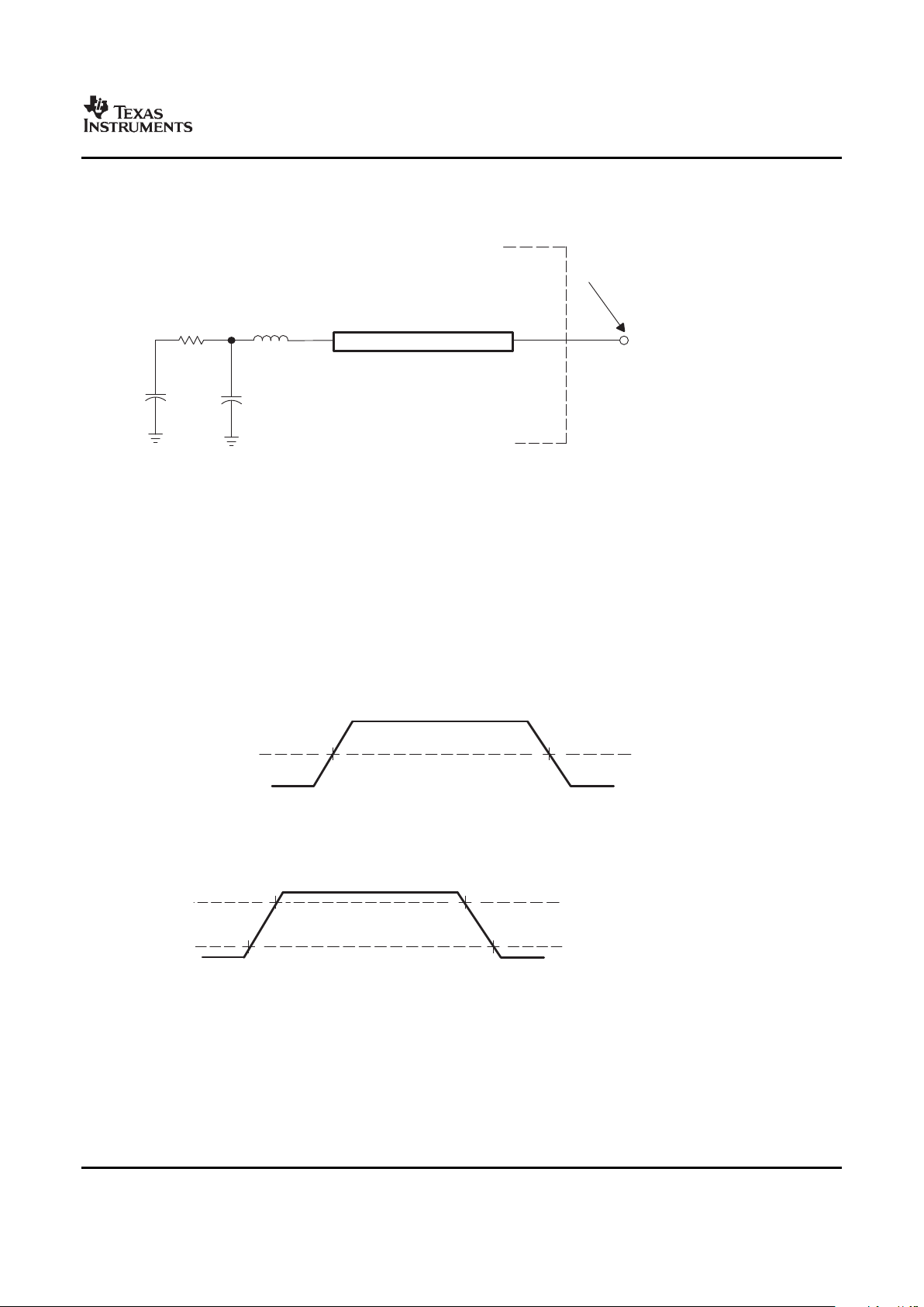
www.ti.com
5 Peripheral Information and Electrical Specifications
5.1 Parameter Information Device-Specific Information
TransmissionLine
4.0pF 1.85pF
Z0=50 Ω
(seenote)
Tester PinElectronics
Data SheetTimingReferencePoint
Output
Under
Test
42 Ω 3.5nH
DevicePin
(seenote)
5.1.1 Signal Transition Levels
V
ref
V
ref
=VILMAX(orVOLMAX)
V
ref
=VIHMIN(orVOHMIN)
TMS320DM355
Digital Media System-on-Chip (DMSoC)
SPRS463 – SEPTEMBER 2007
A. The data sheet provides timing at the device pin. For output timing analysis, the tester pin electronics and its
transmission line effects must be taken into account. A transmission line with a delay of 2 ns or longer can be used to
produce the desired transmission line effect. The transmission line is intended as a load only. It is not necessary to
add or subtract the transmission line delay (2 ns or longer) from the data sheet timings.
Input requirements in this data sheet are tested with an input slew rate of < 4 Volts per nanosecond (4 V/ns) at the
device pin.
Figure 5-1. Test Load Circuit for AC Timing Measurements
The load capacitance value stated is only for characterization and measurement of AC timing signals. This
load capacitance value does not indicate the maximum load the device is capable of driving.
All input and output timing parameters are referenced to V
ref
for both "0" and "1" logic levels. For 3.3 V I/O,
V
ref
= 1.65 V. For 1.8 V I/O, V
ref
= 0.9 V.
Figure 5-2. Input and Output Voltage Reference Levels for AC Timing Measurements
All rise and fall transition timing parameters are referenced to V
IL
MAX and V
IH
MIN for input clocks,
V
OL
MAX and V
OH
MIN for output clocks.
Figure 5-3. Rise and Fall Transition Time Voltage Reference Levels
Submit Documentation Feedback Peripheral Information and Electrical Specifications 93
Page 94

www.ti.com
PRODUCT PREVIEW
5.1.2 Timing Parameters and Board Routing Analysis
TMS320DM355
Digital Media System-on-Chip (DMSoC)
SPRS463 – SEPTEMBER 2007
The timing parameter values specified in this data sheet do not include delays by board routings. As a
good board design practice, such delays must always be taken into account. Timing values may be
adjusted by increasing/decreasing such delays. TI recommends utilizing the available I/O buffer
information specification (IBIS) models to analyze the timing characteristics correctly. To properly use IBIS
models to attain accurate timing analysis for a given system, see the Using IBIS Models for Timing
Analysis application report (literature number SPRA839). If needed, external logic hardware such as
buffers may be used to compensate any timing differences.
94 Peripheral Information and Electrical Specifications Submit Documentation Feedback
Page 95
www.ti.com
5.2 Recommended Clock and Control Signal Transition Behavior
5.3 Power Supplies
TMS320DM355
Digital Media System-on-Chip (DMSoC)
SPRS463 – SEPTEMBER 2007
All clocks and control signals should transition between V
IH
and V
IL
(or between V
IL
and VIH) in a
monotonic manner.
The power supplies of DM355 are summarized in Table 5-1 .
Table 5-1. Power Supplies
Customer Tolerance Package Chip Plane Description Comments
Board Plane Name
Supply
1.3 V ± 5% 1.3 V CV
DD
Core V
DD
V
DDA_PLL1
PLL1 V
DDA
V
DDA_PLL2
PLL2 V
DDA
V
DDD13_USB
USB 1.3 V supply
V
DDA13_USB
USB 1.3 V supply
3.3 V ± 5% 3.3 V V
DD
IO V
DD
for LVCMOS V
DDSHV
V
DD
IO V
DD
for MXI/O1 V
DDSHV
V
DD
IO V
DD
for MXI/O2 V
DDSHV1
V
DD
IO V
DD
for ISB DRVVBUS V
DDSHV2
V
DDA33_DDRDLL
DDR DLL analog V
DD
V
DDA33_USB
Analog 3.3 V power USB PHY
V
DDA33_USB_PLL
Common mode 3.3 V power for USB
PHY (PLL)
V
DD
IO V
DD
for peripherals
3.3 V ± 5% 3.3 V V
DD_VIN
IO V
DD
for VideoIN I/F
V
DD_VOUT
IO V
DD
for VideoOUT I/F
1.8 V ± 5% 1.8 V V
DD_DDR
1.8 V ± 5% 1.8 V V
DDA18
Analog 1.8 V power
1.8 V ± 5% 1.8 V V
DDA18_DAC
Place decoupling caps (0.1 μ F/10 μ f) close
to chip
0 V n/a 0 V V
SS_MX1
Connect to external crystal capacitor
ground
0 V n/a 0 V V
SS_MX2
Connect to external crystal capacitor
ground
0 V n/a 0 V V
SS
Chip ground
USB ESD ground
ground V
SS
0 V n/a 0 V V
SSA
ground Keep separate from digital ground V
SS
0 V n/a 0 V V
SA_PLL1
PLL1 V
SSA
0 V n/a 0 V V
SSA_PLL2
PLL2 V
SSA
0 V n/a 0 V V
SSA_DLL
DLL ground
0 V n/a 0 V V
SS_USB
USB ground V
SSA13_USB
V
SSA13_USB
V
SSA33_USB
V
SSA33_USB_PLL
0 V n/a 0 V V
SS_USB_REF
USB PHY reference ground V
SSREF
0 V n/a 0 V V
SSA_DAC
DAC ground Keep separate from digital ground V
SS
V
DDS
*0.5 V
DDS
*0.5 V
REFSSTL
DRR ref voltage V
DDS
divided by 2, through board resistors
5 V 5 V USB_VBUS VBUS Connect to external charge pump
Submit Documentation Feedback Peripheral Information and Electrical Specifications 95
Page 96

www.ti.com
PRODUCT PREVIEW
5.3.1 Power-Supply Sequencing
TMS320DM355
Digital Media System-on-Chip (DMSoC)
SPRS463 – SEPTEMBER 2007
In order to ensure device reliability, the DM355 requires the following power supply power-on and
power-off sequences. See table Table 5-1 for a description of DM355 power supplies.
Power-On:
1. Power on 1.3 V: CV
DD
, V
DDA_PLL1/2
, V
DDD13_USB
, V
DDA13_USB
2. Power on 1.8 V: V
DD_DDR
, V
DDA18
, V
DDA18_DAC
3. Power on 3.3 V: D
VDD
, V
DDA33_DDRDLL
, V
DDA33_USB
, V
DDA33_USBPLL
, V
DD_VIN
, V
DD_VOUT
You may power-on the 1.8 V and 3.3 V power supplies simultaneously.
Power-Off:
1. Power off 3.3 V: D
VDD
, V
DDA33_DDRDLL
, V
DDA33_USB
, V
DDA33_USBPLL
, V
DD_VIN
, V
DD_VOUT
2. Power off 1.8 V: V
DD_DDR
, V
DDA18
, V
DDA18_DAC
3. Power off 1.3 V: CV
DD
, V
DDA_PLL1/2
, V
DDD13_USB
, V
DDA13_USB
You may power-off the 1.8 V and 3.3 V power supplies simultaneously.
Note that when booting the DM355 from OneNAND, you must ensure that the OneNAND device is ready
with valid program instructions before the DM355 attempts to read program instructions from it. In
particular, before you release DM355 reset, you must allow time for OneNAND device power to stabilize
and for the OneNAND device to complete its internal copy routine. During the internal copy routine, the
OneNAND device copies boot code from its internal non-volatile memory to its internal boot memory
section. Board designers typically achieve this requirement by design of the system power and reset
supervisor circuit. Refer to your OneNAND device datasheet for OneNAND power ramp and stabilization
times and for OneNAND boot copy times.
5.3.1.1 Power-Supply Design Considerations
Core and I/O supply voltage regulators should be located close to the DM355 to minimize inductance and
resistance in the power delivery path. Additionally, when designing for high-performance applications
utilizing the device, the PC board should include separate power planes for core, I/O, and ground, all
bypassed with high-quality low-ESL/ESR capacitors.
5.3.1.2 Power-Supply Decoupling
In order to properly decouple the supply planes from system noise, place as many capacitors (caps) as
possible close to . These caps need to be close to the power pins, no more than 1.25 cm maximum
distance to be effective. Physically smaller caps, such as 0402, are better because of their lower parasitic
inductance. Proper capacitance values are also important. Small bypass caps (near 560 pF) should be
closest to the power pins. Medium bypass caps (220 nF or as large as can be obtained in a small
package) should be next closest. TI recommends no less than 8 small and 8 medium caps per supply be
placed immediately next to the BGA vias, using the "interior" BGA space and at least the corners of the
"exterior".
Larger caps for each supply can be placed further away for bulk decoupling. Large bulk caps (on the order
of 100 μ F) should be furthest away, but still as close as possible. Large caps for each supply should be
placed outside of the BGA footprint.
Any cap selection needs to be evaluated from a yield/manufacturing point-of-view. As with the selection of
any component, verification of capacitor availability over the product’s production lifetime should be
considered. See also Section 5.5.1 and Section 5.5.2 for additional recommendations on power supplies
for the oscillator/PLL supplies.
Peripheral Information and Electrical Specifications96 Submit Documentation Feedback
Page 97

www.ti.com
5.4 Reset
5.4.1 Reset Electrical Data/Timing
1
2
3
RESET
BootConfigurationPins
(BTSEL[1:0],AECFG[3:0])
TMS320DM355
Digital Media System-on-Chip (DMSoC)
SPRS463 – SEPTEMBER 2007
Table 5-2. Timing Requirements for Reset
(1) (2)
(see Figure 5-4 )
DM355
NO. UNIT
MIN MAX
1 t
w(RESET)
Active low width of the RESET pulse 12C ns
2 t
su(BOOT)
Setup time, boot configuration pins valid before RESET rising edge 12C ns
3 t
h(BOOT)
Hold time, boot configuration pins valid after RESET rising edge 12C ns
(1) BTSEL[1:0] and AECFG[4:0] are the boot configuration pins during device reset.
(2) C = MXI/CLKIN cycle time in ns. For example, when MXI/CLKIN frequency is 24 MHz use C = 41. 6 ns.
Figure 5-4. Reset Timing
Submit Documentation Feedback Peripheral Information and Electrical Specifications 97
Page 98

www.ti.com
PRODUCT PREVIEW
5.5 Oscillators and Clocks
5.5.1 MXI1 (24-MHz) Oscillator
Crystal
24MHzor
36MHz
C1 C2
MXI1/CLKIN
MXO1 V
SS_MX1
0.1 F
1 F
L1
V
DDA_PLL1
V
SSA_PLL1
C
L
C1C
2
(C1C2)
TMS320DM355
Digital Media System-on-Chip (DMSoC)
SPRS463 – SEPTEMBER 2007
has two oscillator input/output pairs (MXI1/MXO1 and MXI2/MXO2) usable with external crystals or
ceramic resonators to provide clock inputs. The optimal frequencies for the crystals are 24 MHz
(MXI1/MXO1) and 27 MHz (MXI2/MXO2). Optionally, the oscillator inputs are configurable for use with
external clock oscillators. If external clock oscillators are used, to minimize the clock jitter, a single clean
power supply should power both the and the external oscillator circuit and the minimum CLKIN rise and
fall times must be observed. The electrical requirements and characteristics are described in this section.
The timing parameters for CLKOUT[3:1] are also described in this section. The has three output clock pins
(CLKOUT[3:1]). See Section 3.5 and Section 3.6 for more information on CLKOUT[3:1].
The MXI1 (typically 24 MHz, can also be 36 MHz) oscillator provides the primary reference clock for the
device. The on-chip oscillator requires an external crystal connected across the MXI1 and MXO1 pins,
along with two load capacitors, as shown in Figure 5-5 . The external crystal load capacitors must be
connected only to the oscillator ground pin (V
SS_MX1
). Do not connect to board ground (V
SS
). Also, the PLL
power pin (V
DDA_PLL1
) should be connected to the power supply through a ferrite bead, L1 in the example
circuit shown in Figure 5-5 .
Figure 5-5. MXI1 (24-MHz) Oscillator
The load capacitors, C1 and C2, should be chosen such that the equation is satisfied (typical values are
C1 = C2 = 10 pF). CL in the equation is the load specified by the crystal manufacturer. All discrete
components used to implement the oscillator circuit should be placed as close as possible to the
associated oscillator pins (MXI1 and MXO1) and to the V
SS_MX1
pin.
Peripheral Information and Electrical Specifications98 Submit Documentation Feedback
Page 99

www.ti.com
5.5.2 MXI2 (27-MHz) Oscillator (optional oscillator)
Crystal
27MHz
C1 C2
MXI2
MXO2 V
SS_MX2
L1
V
DDA_PLL2
V
SSA_PLL2
0.1 F
1 F
C
L
C1C
2
(C1C2)
TMS320DM355
Digital Media System-on-Chip (DMSoC)
SPRS463 – SEPTEMBER 2007
Table 5-3. Switching Characteristics Over Recommended Operating Conditions for 24-MHz System
Oscillator
PARAMETER MIN TYP MAX UNIT
Start-up time (from power up until oscillating at stable frequency) 4 ms
Oscillation frequency 24 or 36 MHz
ESR 60 Ω
Frequency stability +/-50 ppm
The MXI2 (27 MHz) oscillator provides an optional reference clock for the 's VPSS module. The on-chip
oscillator requires an external 27-MHz crystal connected across the MXI2 and MXO2 pins, along with two
load capacitors, as shown in Figure 5-6 . The external crystal load capacitors must be connected only to
the 27-MHz oscillator ground pin (V
SS_MX2
). Do not connect to board ground (V
SS
). Also, the PLL power
pin (V
DDA_PLL2
) should be connected to the power supply through a ferrite bead, L1 in the example circuit
shown in Figure 5-6 .
Figure 5-6. MXI2 (27-MHz) System Oscillator
The load capacitors, C1 and C2, should be chosen such that the equation is satisfied (typical values are
C1 = C2 = 10 pF). CL in the equation is the load specified by the crystal manufacturer. All discrete
components used to implement the oscillator circuit should be placed as close as possible to the
associated oscillator pins (MXI and MXO) and to the V
SS_MX2
pin.
Table 5-4. Switching Characteristics Over Recommended Operating Conditions for 27-MHz System
Oscillator
PARAMETER MIN TYP MAX UNIT
Start-up time (from power up until oscillating at stable frequency) 4 ms
Oscillation frequency 27 MHz
ESR 60 Ω
Frequency stability +/-50 ppm
Submit Documentation Feedback Peripheral Information and Electrical Specifications 99
Page 100

www.ti.com
PRODUCT PREVIEW
5.5.3 Clock PLL Electrical Data/Timing (Input and Output Clocks)
MXI/CLKIN
2
3
4
4
5
1
MXI/CLKIN
2
3
4
4
5
1
TMS320DM355
Digital Media System-on-Chip (DMSoC)
SPRS463 – SEPTEMBER 2007
Table 5-5. Timing Requirements for MXI1/CLKIN1
(1) (2)
(see Figure 5-7 )
DM355
NO
UNIT
.
MIN TYP MAX
1 t
c(MXI1)
Cycle time, MXI1/CLKIN1 27. 7
(3)
41. 6
(3)
ns
2 t
w(MXI1H)
Pulse duration, MXI1/CLKIN1 high 0.45C 0.55C ns
3 t
w(MXI1L)
Pulse duration, MXI1/CLKIN1 low 0.45C 0.55C ns
4 t
t(MXI1)
Transition time, MXI1/CLKIN1 0.05C ns
5 t
J(MXI1)
Period jitter, MXI1/CLKIN1 0.02C ns
(1) The reference points for the rise and fall transitions are measured at VILMAX and VIHMIN.
(2) C = MXI1/CLKIN1 cycle time in ns. For example, when MXI1/CLKIN1 frequency is 24 MHz use C = 41. 6 ns.
(3) tc(MXI1) = 41. 6 ns and tc(MXI1) = 27. 7 ns are the only supported cycle times for MXI1/CLKIN1.
Figure 5-7. MXI1/CLKIN1 Timing
Table 5-6. Timing Requirements for MXI2/CLKIN2
(1) (2)
(see Figure 5-7 )
NO. DM355 UNIT
MIN TYP MAX
1 t
c(MXI2)
Cycle time, MXI2/CLKIN2 37. 037
(3)
37. 037
(3)
ns
2 t
w(MXI2H)
Pulse duration, MXI2/CLKIN2 high 0.45C 0.55C ns
3 t
w(MXI2L)
Pulse duration, MXI2/CLKIN2 low 0.45C 0.55C ns
4 t
t(MXI2)
Transition time, MXI2/CLKIN2 0.05C ns
5 t
J(MXI2)
Period jitter, MXI2/CLKIN2 0.02C ns
(1) The reference points for the rise and fall transitions are measured at VILMAX and VIHMIN.
(2) C = MXI2/CLKIN2 cycle time in ns. For example, when MXI2/CLKIN2 frequency is 27 MHz use C = 37. 037 ns.
(3) tc(MXI2) = 37. 037 ns is the only supported cycle time for MXI2/CLKIN2.
Figure 5-8. MXI2/CLKIN2 Timing
Peripheral Information and Electrical Specifications100 Submit Documentation Feedback
 Loading...