

Datasheet TMS427409ADJ-70, TMS427409ADJ-60, TMS427409ADJ-50, TMS427409ADGA-70, TMS427409ADGA-60 Datasheet (NATIONAL SEMICONDUCTOR)
...Page 1
The TMS41x409A and TMS42x409A series are
16 777216-bit dynamic random-access memory
(DRAM) devices organized as 4194304 words of
four bits each.
These devices feature maximum RAS
access
times of 50, 60, and 70 ns. All address and data-in
lines are latched on chip to simplify system
design. Data out is unlatched to allow greater
system flexibility .
description
TMS416409A, TMS417409A, TMS426409A, TMS427409A
4194304 BY 4-BIT EXTENDED DATA OUT
DYNAMIC RANDOM-ACCESS MEMORIES
SMKS893B – AUGUST 1996 – REVISED APRIL 1997
1
POST OFFICE BOX 1443 • HOUSTON, TEXAS 77251–1443
This data sheet is applicable to all
TMS41x409As and TMS42x409As symbolized
by Revision “B”, Revision “E”, and subsequent
revisions as described in the device
symbolization section.
D
Organization...4194304× 4
D
Single Power Supply (5 V or 3.3 V)
D
Performance Ranges:
ACCESS ACCESS ACCESS EDO
TIME TIME TIME CYCLE
t
RACtCAC
t
AA
t
HPC
MAX MAX MAX MIN
’41x409A-50 50 ns 13 ns 25 ns 20 ns
’41x409A-60 60 ns 15 ns 30 ns 25 ns
’41x409A-70 70 ns 18 ns 35 ns 30 ns
’42x409A-50 50 ns 13 ns 25 ns 20 ns
’42x409A-60 60 ns 15 ns 30 ns 25 ns
’42x409A-70 70 ns 18 ns 35 ns 30 ns
D
Extended-Data-Out (EDO) Operation
D
CAS-Before-RAS (CBR) Refresh
D
Low Power Dissipation
D
3-State Unlatched Output
D
High-Reliability Plastic 24/26-Lead
300-Mil-Wide Surface-Mount Small-Outline
J-Lead (SOJ) Package (DJ Suffix) and
24/26-Lead 300-Mil-Wide Surface-Mount
Thin Small-Outline Package (TSOP)
(DGA Suffix)
D
Operating Free-Air Temperature Range
0°C to 70°C
AVAILABLE OPTIONS
DEVICE
POWER
SUPPLY
SELF
REFRESH,
BATTERY
BACKUP
REFRESH
CYCLES
TMS416409A 5 V – 4096 in 64 ms
TMS417409A 5 V – 2048 in 32 ms
TMS426409A 3.3 V – 4096 in 64 ms
TMS427409A 3.3 V – 2048 in 32 ms
The TMS416409A and TMS417409A are offered in a 24/26-lead plastic surface-mount SOJ package
(DJ suffix). The TMS426409A and TMS427409A are offered in a 24/26-lead plastic surface-mount SOJ
package (DJ suffix) and a 24/26-lead plastic surface-mount TSOP (DGA suffix). These packages are designed
for operation from 0°C to 70°C.
Please be aware that an important notice concerning availability, standard warranty, and use in critical applications of
Texas Instruments semiconductor products and disclaimers thereto appears at the end of this data sheet.
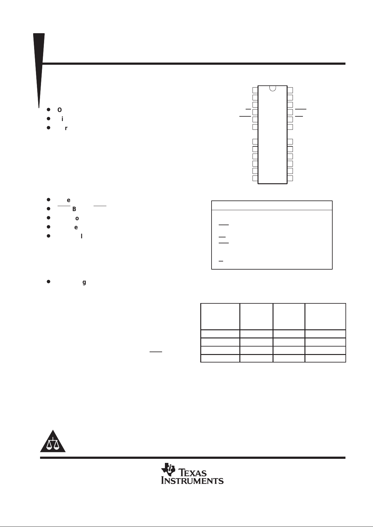
PIN NOMENCLATURE
A0–A11
†
Address Inputs
DQ1–DQ4 Data In/Data Out
CAS
Column-Address Strobe
NC No Internal Connection
OE
Output Enable
RAS
Row-Address Strobe
V
CC
5-V or 3.3-V Supply
‡
V
SS
Ground
W
Write Enable
†
A11 is NC for TMS417409A and TMS427409A.
‡
See Available Options Table
DJ/DGA PACKAGES
(TOP VIEW)
V
CC
DQ1
DQ2
W
RAS
A0
A1
A2
A3
V
CC
V
SS
DQ4
DQ3
CAS
OE
A7
A6
A5
A4
V
SS
26
25
24
23
22
18
17
16
15
14
1
2
3
4
5
9
10
11
12
13
A1 1
†
A9
216
A10 A8198
Copyright 1997, Texas Instruments Incorporated
PRODUCTION DATA information is current as of publication date.
Products conform to specifications per the terms of Texas Instruments
standard warranty. Production processing does not necessarily include
testing of all parameters.
Page 2
TMS416409A, TMS417409A, TMS426409A, TMS427409A
4194304 BY 4-BIT EXTENDED DATA OUT
DYNAMIC RANDOM-ACCESS MEMORIES
SMKS893B – AUGUST 1996 – REVISED APRIL 1997
2
POST OFFICE BOX 1443 • HOUSTON, TEXAS 77251–1443
logic symbol (TMS416409A and TMS426409A)
†
A0
A1
A2
A3
A4
A5
A6
A7
A8
RAS
CAS
W
OE
9
10
11
12
19
15
16
17
18
5
23
4
22
20D10/21D0
20D19/21D9
C20 [ROW]
G23/[REFRESH ROW]
24 [PWR DWN]
C21[COLUMN]
G24
23C22
23,21D 24,25 EN
G25
A
0
4194303
RAM 4096 K × 4
&
A9
21
2
3
24
25
A,Z26
A,22D
26
DQ1
DQ2
DQ3
DQ4
A10
8
20D21
A11
6
20D20
†
This symbol is in accordance with ANSI/IEEE Std 91-1984 and IEC Publication 647-12.
Page 3
TMS416409A, TMS417409A, TMS426409A, TMS427409A
4194304 BY 4-BIT EXTENDED DATA OUT
DYNAMIC RANDOM-ACCESS MEMORIES
SMKS893B – AUGUST 1996 – REVISED APRIL 1997
3
POST OFFICE BOX 1443 • HOUSTON, TEXAS 77251–1443
logic symbol (TMS417409A and TMS427409A)
†
A0
A1
A2
A3
A4
A5
A6
A7
A8
RAS
CAS
W
OE
9
10
11
12
19
15
16
17
18
5
23
4
22
20D11/21D0
C20 [ROW]
G23/[REFRESH ROW]
24 [PWR DWN]
C21[COLUMN]
G24
23C22
23,21D 24,25 EN
G25
A
0
4194303
RAM 4096 K × 4
&
A9
21
2
3
24
25
A,Z26
A,22D
26
DQ1
DQ2
DQ3
DQ4
A10
8
20D21/21D10
†
This symbol is in accordance with ANSI/IEEE Std 91-1984 and IEC Publication 647-12.
Page 4
TMS416409A, TMS417409A, TMS426409A, TMS427409A
4194304 BY 4-BIT EXTENDED DATA OUT
DYNAMIC RANDOM-ACCESS MEMORIES
SMKS893B – AUGUST 1996 – REVISED APRIL 1997
4
POST OFFICE BOX 1443 • HOUSTON, TEXAS 77251–1443
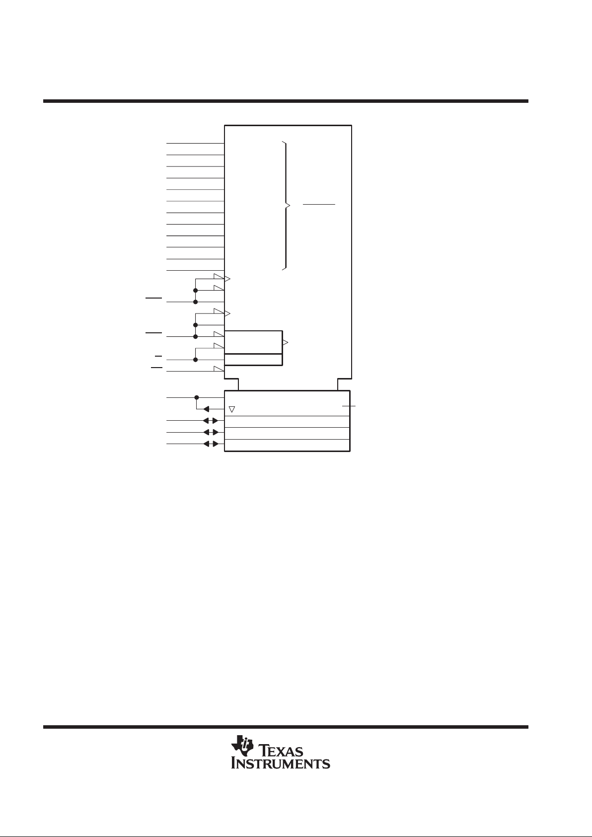
functional block diagram
TMS416409A, TMS426409A
R
o
w
D
e
c
o
d
e
A0
A1
A11
Timing and Control
ColumnAddress
Buffers
†
Row-
Address
Buffers
I/O
Buffers
Data-
In
Reg.
Data-
Out
Reg.
Column Decode
Sense Amplifiers
64
256K Array
256K Array
256K Array
RAS
CAS W
DQ1–DQ4
4
4
OE
10
12
12
4
4
†
Column addresses A10 and A11 are not used.
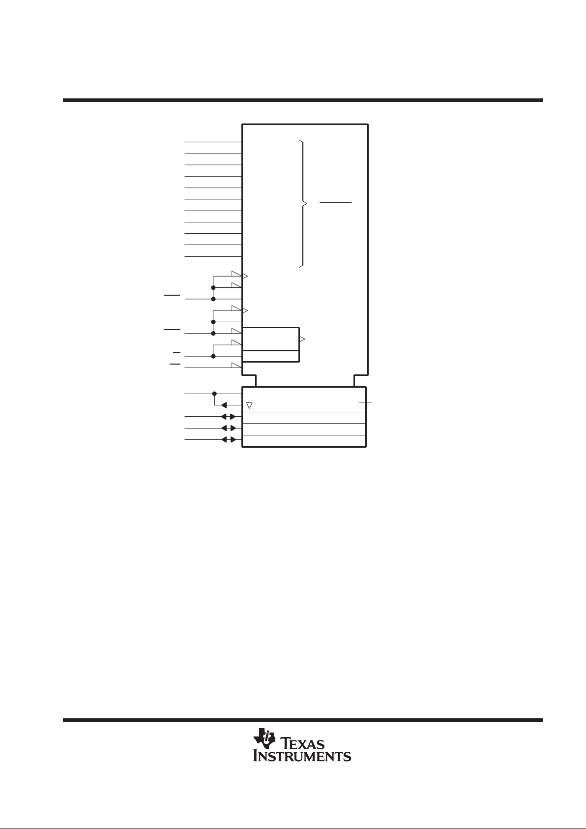
TMS417409A, TMS427409A
A0
A1
A10
32
Timing and Control
ColumnAddress
Buffers
Row-
Address
Buffers
I/O
Buffers
Data-
In
Reg.
Data-
Out
Reg.
Column Decode
Sense Amplifiers
R
o
w
D
e
c
o
d
e
32
256K Array
256K Array
256K Array
256K Array
256K Array
256K Array
RAS
CAS W
DQ1–DQ4
4
4
OE
11
11
11
4
4
Page 5

TMS416409A, TMS417409A, TMS426409A, TMS427409A
4194304 BY 4-BIT EXTENDED DATA OUT
DYNAMIC RANDOM-ACCESS MEMORIES
SMKS893B – AUGUST 1996 – REVISED APRIL 1997
5
POST OFFICE BOX 1443 • HOUSTON, TEXAS 77251–1443
operation
extended data out
Extended data out (EDO) allows data output rates of up to 50 MHz for 50-ns devices. When keeping the same
row address while selecting random column addresses, the time for row-address setup and hold and for address
multiplex is eliminated. The maximum number of columns that can be accessed is determined by t
RASP
, the
maximum RAS
low time.
Extended data out does not place the data in/data out pins (DQ pins) into the high-impedance state with the
rising edge of CAS
. The output remains valid for the system to latch the data. After CAS goes high, the DRAM
decodes the next address. OE
and W can control the output impedance. Descriptions of OE and W further
explain EDO operation benefit.
address: A0–A11 (TMS416409A and TMS426409A) and A0–A10 (TMS417409A and TMS427409A)
Twenty-two address bits are required to decode each of the 4194304 storage cell locations. For the
TMS416409A and TMS426409A,12 row-address bits are set up on A0 through A1 1 and latched onto the chip
by the row-address strobe (RAS
). T en column-address bits are set up on A0 through A9. For the TMS417409A
and TMS427409A, 1 1 row-address bits are set up on inputs A0 through A10 and latched onto the chip by RAS
.
Eleven column-address bits are set up on A0 through A10. All addresses must be stable on or before the falling
edge of RAS
and CAS. RAS is similar to a chip enable because it activates the sense amplifiers as well as the
row decoder. CAS
is used as a chip select, activating the output buffers and latching the address bits into the
column-address buffers.
output enable (OE
)
OE
controls the impedance of the output buffers. While CAS and RAS are low and W is high, OE can be brought
low or high and the DQs transition between valid data and high impedance (see Figure 8). There are two
methods for placing the DQs into the high-impedance state and maintaining that state during CAS
high time.
The first method is to transition OE
high before CAS transitions high and keep OE high for t
CHO
(hold time, OE
from CAS) past the CAS transition. This disables the DQs and they remain disabled, regardless of OE, until CAS
falls again. The second method is to have OE low as CAS transitions high. Then OE can pulse high for a
minimum of t
OEP
(precharge time, OE) anytime during CAS high time, disabling the DQs regardless of further
transitions on OE
until CAS falls again (see Figure 8).
write enable (W
)
The read or write mode is selected through W
. A logic high on W selects the read mode, and a logic low selects
the write mode. The data inputs are disabled when the read mode is selected. When W
goes low prior to CAS
(early write), data out remains in the high-impedance state for the entire cycle, permitting a write operation with
OE
grounded. If W goes low in an extended-data-out read cycle, the DQs are disabled so long as CAS is high
(see Figure 9).
data in/data out (DQ1–DQ4)
Data is written during a write or read-modify-write cycle. Depending on the mode of operation, the later falling
edge of CAS
or W strobes data into the on-chip data latch with setup and hold times referenced to the later edge.
The DQs drive valid data after all access times are met and remain valid except in cases described in the W
and OE sections.
Page 6

TMS416409A, TMS417409A, TMS426409A, TMS427409A
4194304 BY 4-BIT EXTENDED DATA OUT
DYNAMIC RANDOM-ACCESS MEMORIES
SMKS893B – AUGUST 1996 – REVISED APRIL 1997
6
POST OFFICE BOX 1443 • HOUSTON, TEXAS 77251–1443
RAS-only refresh
TMS416409A, TMS426409A
A refresh operation must be performed at least once every 64 ms to retain data. This can be achieved by strobing
each of the 4096 rows (A0–A11). A normal read or write cycle refreshes all bits in each row that is selected.
A RAS
-only operation can be used by holding CAS at the high (inactive) level, conserving power as the output
buffers remain in the high-impedance state. Externally generated addresses must be used for a RAS
-only
refresh.
TMS417409A, TMS427409A
A refresh operation must be performed at least once every 32 ms to retain data. This can be achieved by strobing
each of the 2048 rows (A0–A10). A normal read or write cycle refreshes all bits in each row that is selected.
A RAS
-only operation can be used by holding CAS at the high (inactive) level, conserving power as the output
buffers remain in the high-impedance state. Externally generated addresses must be used for a RAS
-only
refresh.
hidden refresh
A hidden refresh can be performed while maintaining valid data at the output pin. This is accomplished by
holding CAS
at VIL after a read operation and cycling RAS after a specified precharge period, similar to a
RAS
-only refresh cycle. The external address is ignored, and the refresh address is generated internally.
CAS
-before-RAS (CBR) refresh
CBR refresh is performed by bringing CAS
low earlier than RAS (see parameter t
CSR
) and holding it low after
RAS
falls (see parameter t
CHR
). For successive CBR refresh cycles, CAS can remain low while cycling RAS.
The external address is ignored, and the refresh address is generated internally.
power up
T o achieve proper device operation, an initial pause of 200 µs followed by a minimum of eight initialization cycles
is required after power up to the full V
CC
level. These eight initialization cycles must include at least one refresh
(RAS
-only or CBR) cycle.
test mode
The test mode (see Figure 1) is initiated with a CBR-refresh cycle while simultaneously holding the W
input low.
The entry cycle performs an internal refresh cycle while internally setting the device to perform parallel read or
write on subsequent cycles. While in the test mode, any data sequence can be performed. The device exits test
mode if a CBR refresh cycle with W
held high or a RAS-only refresh cycle is performed.
In the test mode, the device is configured as 1024K bits × 4 bits for each DQ. Each DQ pin has a separate 4-bit
parallel read and write data bus that ignores column addresses A0 and A1. During a read cycle, the four internal
bits are compared for each DQ pin. If the four bits agree, DQ goes high; if not, DQ goes low. Test time is reduced
by a factor of four for this series.
Page 7
TMS416409A, TMS417409A, TMS426409A, TMS427409A
4194304 BY 4-BIT EXTENDED DATA OUT
DYNAMIC RANDOM-ACCESS MEMORIES
SMKS893B – AUGUST 1996 – REVISED APRIL 1997
7
POST OFFICE BOX 1443 • HOUSTON, TEXAS 77251–1443
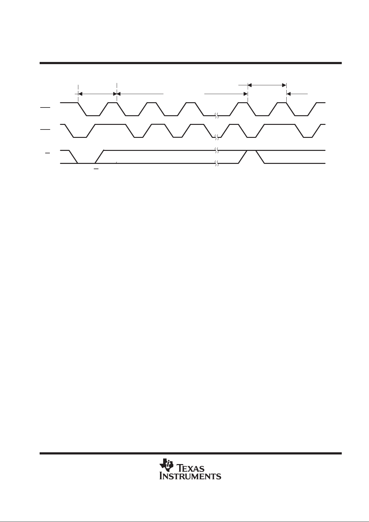
test mode (continued)
Test Mode CycleEntry Cycle
Exit Cycle
Normal
Mode
RAS
CAS
W
NOTE A: The states of W, data in, and address are defined by the type of cycle used during test mode.
Figure 1. Test-Mode Cycle
Page 8
TMS416409A, TMS417409A, TMS426409A, TMS427409A
4194304 BY 4-BIT EXTENDED DATA OUT
DYNAMIC RANDOM-ACCESS MEMORIES
SMKS893B – AUGUST 1996 – REVISED APRIL 1997
8
POST OFFICE BOX 1443 • HOUSTON, TEXAS 77251–1443
absolute maximum ratings over operating free-air temperature range (unless otherwise noted)
†
Supply voltage range, V
CC
(TMS41x409A) – 1 V to 7 V. . . . . . . . . . . . . . . . . . . . . . . . . . . . . . . . . . . . . . . . . . . . . .
Supply voltage range, V
CC
(TMS42x409A) – 0.5 V to 4.6 V. . . . . . . . . . . . . . . . . . . . . . . . . . . . . . . . . . . . . . . . . .
Voltage range on any pin (TMS41x409A) (see Note 1) – 1 V to 7 V. . . . . . . . . . . . . . . . . . . . . . . . . . . . . . . . . . . .
Voltage range on any pin (TMS42x409A) (see Note 1) – 0.5 V to 4.6 V. . . . . . . . . . . . . . . . . . . . . . . . . . . . . . . .
Short-circuit output current 50 mA. . . . . . . . . . . . . . . . . . . . . . . . . . . . . . . . . . . . . . . . . . . . . . . . . . . . . . . . . . . . . . . .
Power dissipation 1 W. . . . . . . . . . . . . . . . . . . . . . . . . . . . . . . . . . . . . . . . . . . . . . . . . . . . . . . . . . . . . . . . . . . . . . . . . .
Operating free-air temperature range, T
A
0°C to 70°C. . . . . . . . . . . . . . . . . . . . . . . . . . . . . . . . . . . . . . . . . . . . . .
Storage temperature range, T
stg
–55°C to 125°C. . . . . . . . . . . . . . . . . . . . . . . . . . . . . . . . . . . . . . . . . . . . . . . . . .
†
Stresses beyond those listed under “absolute maximum ratings” may cause permanent damage to the device. These are stress ratings only, and
functional operation of the device at these or any other conditions beyond those indicated under “recommended operating conditions” is not
implied. Exposure to absolute-maximum-rated conditions for extended periods may affect device reliability.
NOTE 1: All voltage values are with respect to VSS.
recommended operating conditions
TMS41x409A TMS42x409A
MIN NOM MAX MIN NOM MAX UNIT
V
CC
Supply voltage 4.5 5 5.5 3 3.3 3.6 V
V
SS
Supply voltage 0 0 V
V
IH
High-level input voltage 2.4 6.5 2 VCC + 0.3 V
V
IL
Low-level input voltage (see Note 2) –1 0.8 – 0.3 0.8 V
T
A
Operating free-air temperature 0 70 0 70
°C
NOTE 2: The algebraic convention, where the more negative (less positive) limit is designated as minimum, is used for logic-voltage levels only.
Page 9
TMS416409A, TMS417409A, TMS426409A, TMS427409A
4194304 BY 4-BIT EXTENDED DATA OUT
DYNAMIC RANDOM-ACCESS MEMORIES
SMKS893B – AUGUST 1996 – REVISED APRIL 1997
9
POST OFFICE BOX 1443 • HOUSTON, TEXAS 77251–1443
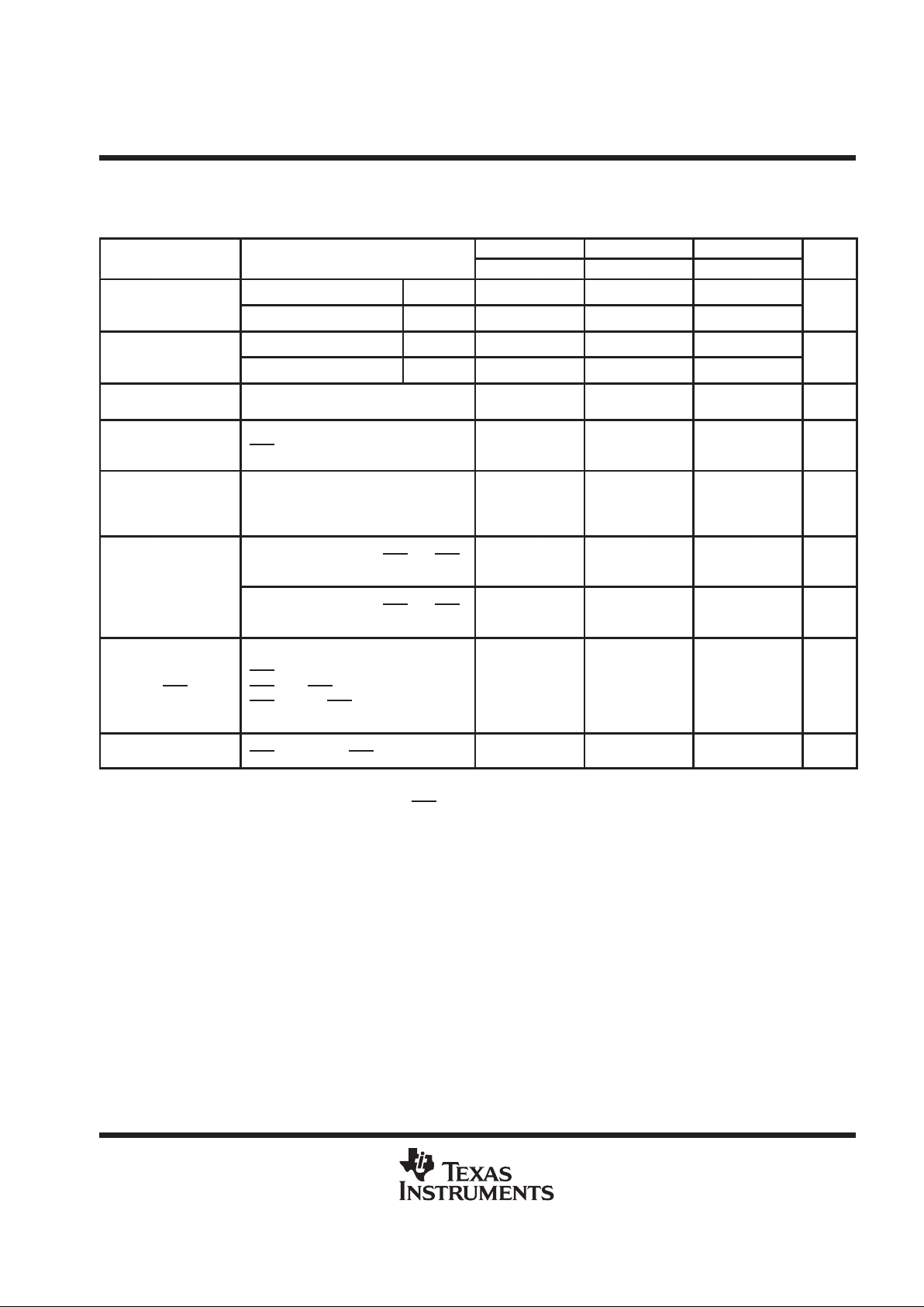
electrical characteristics over recommended ranges of supply voltage and operating free-air
temperature (unless otherwise noted)
TMS416409A
’416409A-50 ’416409A-60 ’416409A-70
PARAMETER
TEST CONDITIONS
†
MIN MAX MIN MAX MIN MAX
UNIT
V
OH
High-level output
voltage
IOH = – 5 mA 2.4 2.4 2.4 V
V
OL
Low-level output voltage IOL = 4.2 mA 0.4 0.4 0.4 V
I
I
Input current (leakage)
VCC = 5.5 V, VI = 0 V to 6.5 V,
All others = 0 V to V
CC
± 10 ± 10 ± 10 µA
I
O
Output current
(leakage)
VCC = 5.5 V, VO = 0 V to VCC,
CAS
high
± 10 ± 10 ± 10 µA
I
CC1
‡§
Average read- or
write-cycle current
VCC = 5.5 V, Minimum cycle 100 80 70 mA
Average standby
VIH = 2.4 V (TTL),
After one memory cycle,
RAS
and CAS high
2 2 2 mA
I
CC2
gy
current
VIH = VCC – 0.2 V (CMOS),
After one memory cycle,
RAS
and CAS high
1 1 1 mA
I
CC3
‡§
Average refresh current
(RAS
-only refresh or
CBR)
VCC = 5.5 V, Minimum cycle,
RAS
cycling,
CAS
high (RAS only),
RAS
low after CAS low (CBR)
100 80 70 mA
I
CC4
‡¶
Average EDO current
VCC = 5.5 V, t
HPC
= MIN,
RAS
low, CAS cycling
100 90 80 mA
†
For conditions shown as MIN/MAX, use the appropriate value specified in the timing requirements.
‡
Measured with outputs open
§
Measured with a maximum of one address change while RAS
= V
IL
¶
Measured with a maximum of one address change during each EDO cycle, t
HPC
Page 10
TMS416409A, TMS417409A, TMS426409A, TMS427409A
4194304 BY 4-BIT EXTENDED DATA OUT
DYNAMIC RANDOM-ACCESS MEMORIES
SMKS893B – AUGUST 1996 – REVISED APRIL 1997
10
POST OFFICE BOX 1443 • HOUSTON, TEXAS 77251–1443
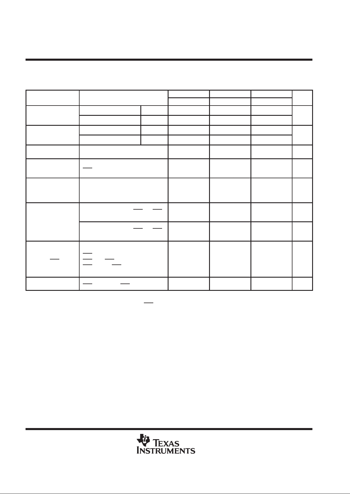
electrical characteristics over recommended ranges of supply voltage and operating free-air
temperature (unless otherwise noted) (continued)
TMS417409A
’417409A-50 ’417409A-60 ’417409A-70
PARAMETER
TEST CONDITIONS
†
MIN MAX MIN MAX MIN MAX
UNIT
V
OH
High-level output
voltage
IOH = – 5 mA 2.4 2.4 2.4 V
V
OL
Low-level output voltage IOL = 4.2 mA 0.4 0.4 0.4 V
I
I
Input current (leakage)
VCC = 5.5 V, VI = 0 V to 6.5 V,
All others = 0 V to V
CC
± 10 ± 10 ± 10 µA
I
O
Output current
(leakage)
VCC = 5.5 V, VO = 0 V to VCC,
CAS
high
± 10 ± 10 ± 10 µA
I
CC1
‡§
Average read- or
write-cycle current
VCC = 5.5 V, Minimum cycle 130 110 100 mA
Average standby
VIH = 2.4 V (TTL),
After one memory cycle,
RAS
and CAS high
2 2 2 mA
I
CC2
gy
current
VIH = VCC – 0.2 V (CMOS),
After one memory cycle,
RAS
and CAS high
1 1 1 mA
I
CC3
‡§
Average refresh current
(RAS
-only refresh or
CBR)
VCC = 5.5 V, Minimum cycle,
RAS
cycling, CAS high (RAS only),
RAS
low after CAS low (CBR)
130 110 100 mA
I
CC4
‡¶
Average EDO current
VCC = 5.5 V, t
HPC
= MIN,
RAS
low, CAS cycling
110 90 80 mA
†
For conditions shown as MIN/MAX, use the appropriate value specified in the timing requirements.
‡
Measured with outputs open
§
Measured with a maximum of one address change while RAS
= V
IL
¶
Measured with a maximum of one address change during each EDO cycle, t
HPC
Page 11
TMS416409A, TMS417409A, TMS426409A, TMS427409A
4194304 BY 4-BIT EXTENDED DATA OUT
DYNAMIC RANDOM-ACCESS MEMORIES
SMKS893B – AUGUST 1996 – REVISED APRIL 1997
11
POST OFFICE BOX 1443 • HOUSTON, TEXAS 77251–1443
electrical characteristics over recommended ranges of supply voltage and operating free-air
temperature (unless otherwise noted) (continued)
TMS426409A
’426409A-50 ’426409A-60 ’426409A-70
PARAMETER
TEST CONDITIONS
†
MIN MAX MIN MAX MIN MAX
UNIT
High-level
p
IOH = – 2 mA LVTTL 2.4 2.4 2.4
V
OH
outpu
t
voltage
IOH = – 100 µA
LVCMOS VCC–0.2 VCC–0.2 VCC–0.2
V
Low-level
p
IOL = 2 mA LVTTL 0.4 0.4 0.4
V
OL
outpu
t
voltage
IOL = 100 µA
LVCMOS 0.2 0.2 0.2
V
I
I
Input current
(leakage)
VCC = 3.6 V, VI = 0 V to 3.9 V,
All others = 0 V to V
CC
± 10 ± 10 ± 10 µA
I
O
Output
current
(leakage)
VCC = 3.6 V, VO = 0 V to VCC,
CAS
high
± 10 ± 10 ± 10 µA
I
CC1
‡§
Average
read- or
write- cycle
current
VCC = 3.6 V, Minimum cycle 90 70 60 mA
Average
VIH = 2 V (LVTTL)
After one memory cycle, RAS
and CAS
high
2 2 2 mA
I
CC2
standby
current
VIH = VCC – 0.2 V (LVCMOS),
After one memory cycle, RAS and CAS
high
1 1 1 mA
I
CC3
‡§
Average
refresh
current
(RAS
-only
refresh
or CBR)
VCC = 3.6 V, Minimum cycle,
RAS
cycling,
CAS
high (RAS-only refresh),
RAS
low after CAS low (CBR)
90 70 60 mA
I
CC4
‡¶
Average
EDO current
VCC = 3.6 V, t
HPC
= MIN,
RAS
low, CAS cycling
100 90 80 mA
†
For conditions shown as MIN/MAX, use the appropriate value specified in the timing requirements.
‡
Measured with outputs open
§
Measured with a maximum of one address change while RAS
= V
IL
¶
Measured with a maximum of one address change during each EDO cycle, t
HPC
Page 12
TMS416409A, TMS417409A, TMS426409A, TMS427409A
4194304 BY 4-BIT EXTENDED DATA OUT
DYNAMIC RANDOM-ACCESS MEMORIES
SMKS893B – AUGUST 1996 – REVISED APRIL 1997
12
POST OFFICE BOX 1443 • HOUSTON, TEXAS 77251–1443
electrical characteristics over recommended ranges of supply voltage and operating free-air
temperature (unless otherwise noted) (continued)
TMS427409A
’427409A-50 ’427409A-60 ’427409A-70
PARAMETER
TEST CONDITIONS
†
MIN MAX MIN MAX MIN MAX
UNIT
High-level
p
IOH = – 2 mA LVTTL 2.4 2.4 2.4
V
OH
outpu
t
voltage
IOH = – 100 µA
LVCMOS VCC–0.2 VCC–0.2 VCC–0.2
V
Low-level
p
IOL = 2 mA LVTTL 0.4 0.4 0.4
V
OL
outpu
t
voltage
IOL = 100 µA
LVCMOS 0.2 0.2 0.2
V
I
I
Input current
(leakage)
VCC = 3.6 V, VI = 0 V to 3.9 V,
All others = 0 V to V
CC
± 10 ± 10 ± 10 µA
I
O
Output
current
(leakage)
VCC = 3.6 V, VO = 0 V to VCC,
CAS
high
± 10 ± 10 ± 10 µA
I
CC1
‡§
Average
read- or
write- cycle
current
VCC = 3.6 V, Minimum cycle 120 100 90 mA
Average
VIH = 2 V (LVTTL)
After one memory cycle, RAS
and CAS
high
2 2 2 mA
I
CC2
standby
current
VIH = VCC – 0.2 V (LVCMOS),
After one memory cycle, RAS and CAS
high
1 1 1 mA
I
CC3
‡§
Average
refresh
current
(RAS
-only
refresh
or CBR)
VCC = 3.6 V, Minimum cycle,
RAS
cycling,
CAS
high (RAS-only refresh),
RAS
low after CAS low (CBR)
120 100 90 mA
I
CC4
‡¶
Average
EDO current
VCC = 3.6 V, t
HPC
= MIN,
RAS
low, CAS cycling
110 90 80 mA
†
For conditions shown as MIN/MAX, use the appropriate value specified in the timing requirements.
‡
Measured with outputs open
§
Measured with a maximum of one address change while RAS
= V
IL
¶
Measured with a maximum of one address change during each EDO cycle, t
HPC
Page 13

TMS416409A, TMS417409A, TMS426409A, TMS427409A
4194304 BY 4-BIT EXTENDED DATA OUT
DYNAMIC RANDOM-ACCESS MEMORIES
SMKS893B – AUGUST 1996 – REVISED APRIL 1997
13
POST OFFICE BOX 1443 • HOUSTON, TEXAS 77251–1443
capacitance over recommended ranges of supply voltage and operating free-air temperature,
f = 1 MHz (see Note 3)
PARAMETER MIN MAX UNIT
C
i(A)
Input capacitance, A0–A11
†
5 pF
C
i(OE)
Input capacitance, OE 7 pF
C
i(RC)
Input capacitance, CAS and RAS 7 pF
C
i(W)
Input capacitance, W 7 pF
C
o
Output capacitance
‡
7 pF
†
A11 is NC (no internal connection) for TMS417409A and TMS427409A.
‡
CAS
and OE = VIH to disable outputs
NOTE 3: VCC = NOM supply voltage ±10%, and the bias on pins under test is 0 V.
switching characteristics over recommended ranges of supply voltage and operating free-air
temperature (see Note 4)
PARAMETER
’41x409A-50
’42x409A-50
’41x409A-60
’42x409A-60
’41x409A-70
’42x409A-70
UNIT
MIN MAX MIN MAX MIN MAX
t
AA
Access time from column address (see Note 5) 25 30 35 ns
t
CAC
Access time from CAS (see Note 5) 13 15 18 ns
t
CPA
Access time from CAS precharge (see Note 5) 28 35 40 ns
t
RAC
Access time from RAS (see Note 5) 50 60 70 ns
t
OEA
Access time from OE (see Note 5) 13 15 18 ns
t
CLZ
Delay time, CAS to output in low impedance 0 0 0 ns
t
REZ
Output buffer turn off delay from RAS (see Note 6) 3 13 3 15 3 18 ns
t
CEZ
Output buffer turn off delay from CAS (see Note 6) 3 13 3 15 3 18 ns
t
OEZ
Output buffer turn off delay from OE (see Note 6) 3 13 3 15 3 18 ns
t
WEZ
Output buffer turn off delay from W (see Note 6) 3 13 3 15 3 18 ns
NOTES: 4. With ac parameters, it is assumed that tT = 2 ns.
5. For TMS42x409A, access times are measured with output reference levels of VOH = 2 V and VOL = 0.8 V.
6. The maximum values of t
REZ
, t
CEZ
, t
OEZ
, and t
WEZ
are specified when the output is no longer driven. Data in should not be driven
until one of the applicable maximum specifications is satisfied.
Page 14

TMS416409A, TMS417409A, TMS426409A, TMS427409A
4194304 BY 4-BIT EXTENDED DATA OUT
DYNAMIC RANDOM-ACCESS MEMORIES
SMKS893B – AUGUST 1996 – REVISED APRIL 1997
14
POST OFFICE BOX 1443 • HOUSTON, TEXAS 77251–1443
EDO timing requirements over recommended ranges of supply voltage and operating free-air
temperature (see Note 4)
’41x409A-50
’42x409A-50
’41x409A-60
’42x409A-60
’41x409A-70
’42x409A-70
UNIT
MIN MAX MIN MAX MIN MAX
t
HPC
Cycle time, EDO page mode, read-write 20 25 30 ns
t
PRWC
Cycle time, EDO read-write 57 68 78 ns
t
CSH
Delay time, RAS active to CAS precharge 40 48 58 ns
t
CHO
Hold time, OE from CAS 7 10 10 ns
t
DOH
Hold time, output from CAS 5 5 5 ns
t
CAS
Pulse duration, CAS active (see Note 7) 8 10000 10 10000 12 10000 ns
t
WPE
Pulse duration, W active (output disable only) 7 7 7 ns
t
OCH
Setup time, OE before CAS 8 10 10 ns
t
CP
Pulse duration, CAS precharge 8 10 10 ns
t
OEP
Precharge time, OE 5 5 5 ns
NOTES: 4: With ac parameters, it is assumed that tT = 2 ns.
7. In a read-write cycle, t
CWD
and t
CWL
must be observed.
Page 15

TMS416409A, TMS417409A, TMS426409A, TMS427409A
4194304 BY 4-BIT EXTENDED DATA OUT
DYNAMIC RANDOM-ACCESS MEMORIES
SMKS893B – AUGUST 1996 – REVISED APRIL 1997
15
POST OFFICE BOX 1443 • HOUSTON, TEXAS 77251–1443
timing requirements over recommended ranges of supply voltage and operating free-air
temperature (see Note 4)
’41x409A-50
’42x409A-50
’41x409A-60
’42x409A-60
’41x409A-70
’42x409A-70
UNIT
MIN MAX MIN MAX MIN MAX
t
RC
Cycle time, random read or write 84 104 124 ns
t
RWC
Cycle time, read-write 111 135 160 ns
t
RASP
Pulse duration, RAS active, fast page mode (see Note 8) 50 100000 60 100 000 70 100000 ns
t
RAS
Pulse duration, RAS active, non-page mode (see Note 8) 50 10 000 60 10 000 70 10 000 ns
t
RP
Pulse duration, RAS precharge 30 40 50 ns
t
WP
Pulse duration, write command 8 10 10 ns
t
ASC
Setup time, column address 0 0 0 ns
t
ASR
Setup time, row address 0 0 0 ns
t
DS
Setup time, data in (see Note 9) 0 0 0 ns
t
RCS
Setup time, read command 0 0 0 ns
t
CWL
Setup time, write command before CAS precharge 8 10 12 ns
t
RWL
Setup time, write command before RAS precharge 8 10 12 ns
t
WCS
Setup time, write command before CAS active
(early-write only)
0 0 0 ns
t
WRP
Setup time, W high before RAS low (CBR refresh only) 10 10 10 ns
t
WTS
Setup time, W low before RAS low (test mode only) 10 10 10 ns
t
CSR
Setup time, CAS referenced to RAS (CBR refresh only) 5 5 5 ns
t
CAH
Hold time, column address 8 10 12 ns
t
DH
Hold time, data in (see Note 9) 8 10 12 ns
t
RAH
Hold time, row address 8 10 10 ns
t
RCH
Hold time, read command referenced to CAS (see Note 10) 0 0 0 ns
t
RRH
Hold time, read command referenced to RAS (see Note 10) 0 0 0 ns
t
WCH
Hold time, write command during CAS active
(early-write only)
8 10 12 ns
t
ROH
Hold time, RAS referenced to OE 8 10 10 ns
t
WRH
Hold time, W high after RAS low (CBR refresh) 10 10 10 ns
t
WTH
Hold time, W low after RAS low (test mode only) 10 10 10 ns
t
CHR
Hold time, CAS referenced to RAS (CBR refresh only) 10 10 10 ns
t
OEH
Hold time, OE command 13 15 18 ns
t
RHCP
Hold time, RAS active from CAS precharge 28 35 40 ns
NOTES: 4. With ac parameters, it is assumed that tT = 2 ns.
8. In a read-write cycle, t
RWD
and t
RWL
must be observed.
9. Referenced to the later of CAS
or W in write operations
10. Either t
RRH
or t
RCH
must be satisfied for a read cycle.
Page 16

TMS416409A, TMS417409A, TMS426409A, TMS427409A
4194304 BY 4-BIT EXTENDED DATA OUT
DYNAMIC RANDOM-ACCESS MEMORIES
SMKS893B – AUGUST 1996 – REVISED APRIL 1997
16
POST OFFICE BOX 1443 • HOUSTON, TEXAS 77251–1443
timing requirements over recommended ranges of supply voltage and operating free-air
temperature (see Note 4) (continued)
’41x409A-50
’42x409A-50
’41x409A-60
’42x409A-60
’41x409A-70
’42x409A-70
UNIT
MIN MAX MIN MAX MIN MAX
t
AWD
Delay time, column address to write command
(read-write only)
42 49 57 ns
t
CPW
Delay time, W low after xCAS precharge (read-write only) 45 54 62 ns
t
CRP
Delay time, CAS precharge to RAS 5 5 5 ns
t
CWD
Delay time, CAS to write command (read-write only) 30 34 40 ns
t
OED
Delay time, OE to data in 13 15 18 ns
t
RAD
Delay time, RAS to column address (see Note 11) 10 25 12 30 12 35 ns
t
RAL
Delay time, column address to RAS precharge 25 30 35 ns
t
CAL
Delay time, column address to CAS precharge 18 20 25 ns
t
RCD
Delay time, RAS to CAS (see Note 11) 12 37 14 45 14 52 ns
t
RPC
Delay time, RAS precharge to CAS 5 5 5 ns
t
RSH
Delay time, CAS active to RAS precharge 8 10 12 ns
t
RWD
Delay time, RAS to write command (read-write only) 67 79 92 ns
t
TAA
Access time from address (test mode) 30 35 40 ns
t
TCPA
Access time, from column precharge (test mode) 35 40 45 ns
t
TRAC
Access time, from RAS (test mode) 55 65 75 ns
t
T
Transition time 2 30 2 30 2 30 ns
’4x6409A 64 64 64 ms
t
REF
Refresh time interval
’4x7409A 32 32 32 ms
NOTES: 4. With ac parameters, it is assumed that tT = 2 ns.
11. The maximum value is specified only to ensure access time.
Page 17

TMS416409A, TMS417409A, TMS426409A, TMS427409A
4194304 BY 4-BIT EXTENDED DATA OUT
DYNAMIC RANDOM-ACCESS MEMORIES
SMKS893B – AUGUST 1996 – REVISED APRIL 1997
17
POST OFFICE BOX 1443 • HOUSTON, TEXAS 77251–1443
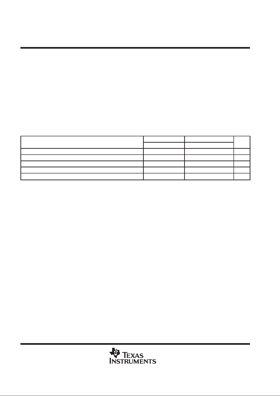
PARAMETER MEASUREMENT INFORMATION
V
TH
V
CC
CL = 100 pF
(see Note A)
Output Under TestOutput Under Test
CL = 100 pF
(see Note A)
(b) ALTERNATE LOAD CIRCUIT(a) LOAD CIRCUIT
NOTE A: CL includes probe and fixture capacitance.
R
L
R
1
R
2
DEVICE VCC (V) R1 (W) R2 (W) VTH (V) RL (W)
’41x409A 5 828 295 1.31 218
’42x409A 3.3 1178 868 1.4 500
Figure 2. Load Circuits for Timing Parameters
Page 18

TMS416409A, TMS417409A, TMS426409A, TMS427409A
4194304 BY 4-BIT EXTENDED DATA OUT
DYNAMIC RANDOM-ACCESS MEMORIES
SMKS893B – AUGUST 1996 – REVISED APRIL 1997
18
POST OFFICE BOX 1443 • HOUSTON, TEXAS 77251–1443
PARAMETER MEASUREMENT INFORMATION
RAS
CAS
Address
W
OE
DQ1–DQ4
t
RC
Row Column
Don’t Care
Don’t Care
Don’t Care
Don’t Care
Don’t Care
Valid Data Out
t
RAS
t
RP
t
CSH
t
T
t
RCD
t
RSH
t
CRP
t
CAS
t
RAD
t
ASC
t
RAL
t
ASR
t
RCS
t
CAH
t
RRH
t
RCH
t
CAC
t
CEZ
t
AA
t
CLZ
t
RAC
t
OEA
t
ROH
t
OEZ
t
CP
See Note A
Hi-Z
t
RAH
t
REZ
t
WEZ
t
WPE
t
CAL
NOTE A: Output can go from the high-impedance state to an invalid-data state prior to the specified access time.
Figure 3. Read-Cycle Timing
Page 19

TMS416409A, TMS417409A, TMS426409A, TMS427409A
4194304 BY 4-BIT EXTENDED DATA OUT
DYNAMIC RANDOM-ACCESS MEMORIES
SMKS893B – AUGUST 1996 – REVISED APRIL 1997
19
POST OFFICE BOX 1443 • HOUSTON, TEXAS 77251–1443
PARAMETER MEASUREMENT INFORMATION
RAS
CAS
Address
W
OE
DQ1–DQ4
t
RC
Row Column
Don’t Care
Don’t Care
Don’t Care
Don’t Care
Valid Data
Don’t Care
t
RP
t
RAS
t
RSH
t
CRP
t
CAS
t
RCD
t
T
t
CSH
t
ASC
t
ASR
t
RAL
t
CAH
t
CP
t
RAD
t
CWL
t
RWL
t
WCH
t
DH
t
DS
t
RAH
t
WCS
t
CAL
Figure 4. Early-Write-Cycle Timing
Page 20

TMS416409A, TMS417409A, TMS426409A, TMS427409A
4194304 BY 4-BIT EXTENDED DATA OUT
DYNAMIC RANDOM-ACCESS MEMORIES
SMKS893B – AUGUST 1996 – REVISED APRIL 1997
20
POST OFFICE BOX 1443 • HOUSTON, TEXAS 77251–1443
PARAMETER MEASUREMENT INFORMATION
RAS
CAS
Address
W
OE
DQ1–DQ4
t
RC
Row Column
Don’t Care
Don’t Care
Don’t Care
Don’t Care
Don’t Care
t
RAS
t
RP
t
RSH
t
CRP
t
CAS
t
RCD
t
CSH
t
T
t
ASR
t
RAH
t
ASC
t
RAL
t
CAH
t
RAD
t
CWL
t
RWL
t
WP
t
CLZ
t
DH
t
OED
t
OEH
t
CP
t
DS
Don’t Care
Invalid Data Out
Valid Data In
t
CAL
Figure 5. Write-Cycle Timing
Page 21

TMS416409A, TMS417409A, TMS426409A, TMS427409A
4194304 BY 4-BIT EXTENDED DATA OUT
DYNAMIC RANDOM-ACCESS MEMORIES
SMKS893B – AUGUST 1996 – REVISED APRIL 1997
21
POST OFFICE BOX 1443 • HOUSTON, TEXAS 77251–1443
PARAMETER MEASUREMENT INFORMATION
RAS
CAS
Address
W
OE
DQ1–DQ4
t
RWC
Row Column
Don’t Care
Don’t Care
Don’t Care
Data
Out
Don’t Care
Don’t Care
Data
In
t
RAS
t
RCD
t
T
t
CAS
t
RP
t
CRP
t
CP
t
T
t
CAH
t
ASC
t
RAH
t
ASR
t
RAD
t
RCS
t
RWD
t
RWL
t
WP
t
AWD
t
CWD
t
CAC
t
DS
t
DH
t
AA
t
CLZ
t
RAC
t
OEA
t
OEZ
t
OED
t
OEH
See Note A
t
CWL
Hi-Z
NOTE A: Output can go from the high-impedance state to an invalid-data state prior to the specified access time.
Figure 6. Read-Write-Cycle Timing
Page 22

TMS416409A, TMS417409A, TMS426409A, TMS427409A
4194304 BY 4-BIT EXTENDED DATA OUT
DYNAMIC RANDOM-ACCESS MEMORIES
SMKS893B – AUGUST 1996 – REVISED APRIL 1997
22
POST OFFICE BOX 1443 • HOUSTON, TEXAS 77251–1443
PARAMETER MEASUREMENT INFORMATION
Data #3Data #2Data #1
Column #3Column #2Column #1Row
DQ1–DQ4
W
OE
Address
CAS
RAS
t
CEZ
t
CLZ
t
ASC
t
CRP
t
CAS
t
RCH
t
DOH
t
CAC
t
RAD
t
CAH
t
RAH
t
ASR
t
CP
t
T
t
RP
t
RCS
t
RAC
t
AA
t
AA
t
CPA
t
REZ
t
RRH
t
OEA
t
RAL
t
RSH
t
HPC
t
CSH
t
RCD
t
RASP
t
CAL
t
CAC
t
RHCP
See Note A
See Note
C
NOTES: A. Output can go from the high-impedance state to an invalid-data state prior to the specified access time.
B. Access time is t
CPA
-, tAA-, or t
CAC
-dependent.
C. Output is turned off by t
CEZ
if RAS
goes high during CAS low.
Figure 7. EDO Read Cycle
Page 23

TMS416409A, TMS417409A, TMS426409A, TMS427409A
4194304 BY 4-BIT EXTENDED DATA OUT
DYNAMIC RANDOM-ACCESS MEMORIES
SMKS893B – AUGUST 1996 – REVISED APRIL 1997
23
POST OFFICE BOX 1443 • HOUSTON, TEXAS 77251–1443
PARAMETER MEASUREMENT INFORMATION
t
OEZ
t
CAC
t
OEA
t
OEP
t
CHO
t
OEP
t
CAH
t
ASC
t
RAH
t
ASR
t
AA
t
CAC
t
CLZ
t
DOH
t
REZ
t
RCH
t
RRH
t
RAD
t
RSH
t
RP
DQ1–DQ4
W
OE
Address
CAS
RAS
t
CPA
t
AA
t
RAC
t
RCS
t
OEA
t
HPC
t
CSH
t
RASP
t
RAL
Row Column #1 Column #2 Column #3
Data #1 Data #1 Data #2 Data #3
t
CAS
t
CP
t
OEZ
t
CEZ
t
OCH
t
RHCP
t
CAL
See Note A
NOTE A: Output is turned off by t
CEZ
if RAS
goes high during CAS low.
Figure 8. EDO Read-Cycle With OE Control
Page 24

TMS416409A, TMS417409A, TMS426409A, TMS427409A
4194304 BY 4-BIT EXTENDED DATA OUT
DYNAMIC RANDOM-ACCESS MEMORIES
SMKS893B – AUGUST 1996 – REVISED APRIL 1997
24
POST OFFICE BOX 1443 • HOUSTON, TEXAS 77251–1443
PARAMETER MEASUREMENT INFORMATION
Column #3Column #2Column #1Row
Data #3Data #2Data #1
DQ1–DQ4
W
OE
Address
CAS
RAS
t
CRP
t
RSH
t
ASR
t
RAH
t
ASC
t
CAH
t
RRH
t
RCH
t
CAC
t
WPE
t
CLZ
t
CAC
t
CEZ
t
REZ
t
WEZ
t
CAS
t
CAC
t
AA
t
CPA
t
AA
t
CPA
t
AA
t
RAC
t
RCS
t
OEA
t
RAD
t
RASP
t
HPC
t
CSH
t
CP
t
RP
t
CAL
t
RHCP
t
DOH
t
RAL
Figure 9. EDO Read-Cycle With W Control
Page 25

TMS416409A, TMS417409A, TMS426409A, TMS427409A
4194304 BY 4-BIT EXTENDED DATA OUT
DYNAMIC RANDOM-ACCESS MEMORIES
SMKS893B – AUGUST 1996 – REVISED APRIL 1997
25
POST OFFICE BOX 1443 • HOUSTON, TEXAS 77251–1443
PARAMETER MEASUREMENT INFORMATION
RAS
CAS
Address
W
OE
DQ1–DQ4
Row Column
Don’t Care
t
RP
Data In
Don’t Care
Don’t Care
Don’t Care
Don’t Care
Column
t
CSH
t
HPC
t
RSH
t
CAS
t
RCD
t
ASC
t
RAH
t
CAH
t
CP
t
ASR
t
WCH
t
CWL
t
RWL
t
DH
t
DS
t
RAL
t
CRP
t
CWL
t
RAD
t
CAL
Don’t Care
Data In
t
RASP
t
RHCP
t
WCS
NOTE A: A read cycle or a read-write cycle can be intermixed with write cycles as long as read and read-write timing specifications are not violated.
Figure 10. EDO Early-Write-Cycle Timing
Page 26

TMS416409A, TMS417409A, TMS426409A, TMS427409A
4194304 BY 4-BIT EXTENDED DATA OUT
DYNAMIC RANDOM-ACCESS MEMORIES
SMKS893B – AUGUST 1996 – REVISED APRIL 1997
26
POST OFFICE BOX 1443 • HOUSTON, TEXAS 77251–1443
PARAMETER MEASUREMENT INFORMATION
RAS
CAS
Address
W
OE
DQ1–DQ4
Row Column
Don’t Care
Don’t Care
Valid
In
t
RP
Valid Data In
Don’t Care
Don’t Care
Don’t Care Don’t Care
Column
t
RASP
t
CSH
t
HPC
t
CRP
t
RSH
t
CAS
t
RCD
t
ASC
t
RAH
t
CAH
t
CP
t
ASR
t
RAD
t
CWL
t
WP
t
OEH
t
OEH
t
OED
t
RAL
t
CAL
t
RHCP
t
DS
t
DH
Don’t Care
t
CLZ
Don’t Care
t
CWL
t
RWL
Invalid Data out
NOTE A: A read cycle or a read-write cycle can be intermixed with write cycles as long as read and read-write timing specifications are not violated.
Figure 11. EDO Write-Cycle Timing
Page 27

TMS416409A, TMS417409A, TMS426409A, TMS427409A
4194304 BY 4-BIT EXTENDED DATA OUT
DYNAMIC RANDOM-ACCESS MEMORIES
SMKS893B – AUGUST 1996 – REVISED APRIL 1997
27
POST OFFICE BOX 1443 • HOUSTON, TEXAS 77251–1443
PARAMETER MEASUREMENT INFORMATION
RAS
CAS
Address
W
OE
DQ1–DQ4
Row Column 1
Don’t Care
Valid
In 2
Column 2
t
RASP
Valid
In 1
t
RP
t
CSH
t
PRWC
t
RCD
t
CP
t
CRP
t
RSH
t
ASC
t
CAH
t
RAD
t
ASR
t
CWD
t
RAH
t
AWD
t
CWL
t
RWL
t
WP
t
RWD
t
CPA
t
OEH
t
DH
t
DS
t
AA
t
RCS
t
RAC
t
CAC
t
CLZ
t
OEA
t
OEZ
t
OEH
t
OED
t
CAS
Valid Out 2
(see Note A)
Valid
Out 1
t
CAL
t
RAL
t
CPW
NOTES: A. Output can go from the high-impedance state to an invalid-data state prior to the specified access time.
B. A read or write cycle can be intermixed with read-write cycles as long as the read- and write-timing specifications are not violated.
Figure 12. EDO Read-Write-Cycle Timing
Page 28

TMS416409A, TMS417409A, TMS426409A, TMS427409A
4194304 BY 4-BIT EXTENDED DATA OUT
DYNAMIC RANDOM-ACCESS MEMORIES
SMKS893B – AUGUST 1996 – REVISED APRIL 1997
28
POST OFFICE BOX 1443 • HOUSTON, TEXAS 77251–1443
PARAMETER MEASUREMENT INFORMATION
t
RC
t
RAS
t
RP
t
T
t
ASR
t
RAH
t
CRP
t
RPC
RAS
CAS
Address
W
DQ1–DQ4
OE
Don’t Care
Don’t Care Row RowDon’t Care
Don’t Care
Hi Z
Don’t Care
Figure 13. RAS-Only Refresh-Cycle Timing
Page 29

TMS416409A, TMS417409A, TMS426409A, TMS427409A
4194304 BY 4-BIT EXTENDED DATA OUT
DYNAMIC RANDOM-ACCESS MEMORIES
SMKS893B – AUGUST 1996 – REVISED APRIL 1997
29
POST OFFICE BOX 1443 • HOUSTON, TEXAS 77251–1443
PARAMETER MEASUREMENT INFORMATION
RAS
CAS
W
Address
OE
DQ1–DQ4
t
RC
Don’t Care
Don’t Care
Hi-Z
t
RAS
t
RP
t
CSR
t
RPC
t
T
t
CHR
t
WRP
t
WRH
Figure 14. Automatic-CBR-Refresh-Cycle Timing
Page 30

TMS416409A, TMS417409A, TMS426409A, TMS427409A
4194304 BY 4-BIT EXTENDED DATA OUT
DYNAMIC RANDOM-ACCESS MEMORIES
SMKS893B – AUGUST 1996 – REVISED APRIL 1997
30
POST OFFICE BOX 1443 • HOUSTON, TEXAS 77251–1443
PARAMETER MEASUREMENT INFORMATION
RAS
CAS
Address
Row Col
Don’t Care
W
OE
DQ1–DQ4
Valid Data Out
t
RAS
t
RP
t
RP
t
RAS
t
CAS
t
CAH
t
ASC
t
RAH
t
ASR
t
RCS
t
RRH
t
WRP
t
WRH
t
WRH
t
WRP
t
CAC
t
AA
t
RAC
t
CEZ
t
CLZ
t
OEA
t
OEZ
t
CHR
Refresh Cycle
Refresh Cycle
Memory Cycle
t
WRH
t
WRP
t
REZ
t
WEZ
Figure 15. Hidden-Refresh-Cycle (Read) Timing
Page 31

TMS416409A, TMS417409A, TMS426409A, TMS427409A
4194304 BY 4-BIT EXTENDED DATA OUT
DYNAMIC RANDOM-ACCESS MEMORIES
SMKS893B – AUGUST 1996 – REVISED APRIL 1997
31
POST OFFICE BOX 1443 • HOUSTON, TEXAS 77251–1443
PARAMETER MEASUREMENT INFORMATION
RAS
CAS
Address
W
DQ1–DQ4
OE
Row Col
Don’t Care
Valid Data
Don’t Care
Don’t Care
Refresh Cycle
Memory Cycle
Refresh Cycle
t
RAS
t
RP
t
RAS
t
RP
t
CHR
t
CAS
t
CAH
t
ASC
t
RAH
t
ASR
t
WCS
t
WP
t
WRP
t
WRH
t
DH
t
DS
t
WCH
Figure 16. Hidden-Refresh-Cycle (Write) Timing
Page 32

TMS416409A, TMS417409A, TMS426409A, TMS427409A
4194304 BY 4-BIT EXTENDED DATA OUT
DYNAMIC RANDOM-ACCESS MEMORIES
SMKS893B – AUGUST 1996 – REVISED APRIL 1997
32
POST OFFICE BOX 1443 • HOUSTON, TEXAS 77251–1443
PARAMETER MEASUREMENT INFORMATION
RAS
CAS
W
Address
OE
DQ1–DQ4
t
RC
Don’t Care
Don’t Care
Hi-Z
t
RAS
t
RP
t
CSR
t
RPC
t
T
t
CHR
t
WTS
t
WTH
Don’t Care
Figure 17. Test-Mode-Entry-Cycle Timing
RAS
CAS
Address
W
DQ1–DQ4
t
RP
t
RC
t
RAS
t
RPC
t
CSR
t
T
t
CHR
t
WRP
t
WRH
Don’t CareDon’t Care
Don’t Care
t
CEZ
Hi-Z
Don’t Care
t
REZ
Figure 18. Test-Mode-Exit-Cycle CBR-Refresh-Cycle Timing
Page 33

TMS416409A, TMS417409A, TMS426409A, TMS427409A
4194304 BY 4-BIT EXTENDED DATA OUT
DYNAMIC RANDOM-ACCESS MEMORIES
SMKS893B – AUGUST 1996 – REVISED APRIL 1997
33
POST OFFICE BOX 1443 • HOUSTON, TEXAS 77251–1443
MECHANICAL DATA
DJ (R-PDSO-J24/26) PLASTIC SMALL-OUTLINE J-LEAD PACKAGE
4040092-3/B 02/95
0.340 (8,64)
0.330 (8,38)
0.106 (2,69) TYP 0.008 (0,20) NOM
0.275 (6,99)
0.260 (6,60)
Seating Plane
14
13
1921
86
0.670 (17,02)
0.680 (17,27)
0.026 (0,66)
0.032 (0,81)
26
1
0.148 (3,76)
0.020 (0,51)
0.016 (0,41)
0.128 (3,25)
0.295 (7,49)
0.305 (7,75)
0.004 (0,10)
M
0.007 (0,18)
0.050 (1,27)
NOTES: A. All linear dimensions are in inches (millimeters).
B. This drawing is subject to change without notice.
C. Plastic body dimensions do not include mold protrusion. Maximum mold protrusion is 0.005 (0,125).
Page 34

TMS416409A, TMS417409A, TMS426409A, TMS427409A
4194304 BY 4-BIT EXTENDED DATA OUT
DYNAMIC RANDOM-ACCESS MEMORIES
SMKS893B – AUGUST 1996 – REVISED APRIL 1997
34
POST OFFICE BOX 1443 • HOUSTON, TEXAS 77251–1443
MECHANICAL DATA
DGA (R-PDSO-G24/26) PLASTIC SMALL-OUTLINE PACKAGE
4040265-3/C 11/95
0.304 (7,72)
0.296 (7,52)
0.047 (1,19) MAX 0.002 (0,05) MIN
1
26
0.679 (17,24)
0.671 (17,04)
13
0.020 (0,50)
0.012 (0,30)
14
0.016 (0,40)
Seating Plane
0.006 (0,15) NOM
0.371 (9,42)
0.355 (9,02)
Gage Plane
0.010 (0,25)
0.024 (0,60)
0.004 (0,10)
M
0.008 (0,21)
0.050 (1,27)
0°–5°
NOTES: A. All linear dimensions are in inches (millimeters).
B. This drawing is subject to change without notice.
C. Body dimensions do not include mold flash or protrusion.
Page 35

TMS416409A, TMS417409A, TMS426409A, TMS427409A
4194304 BY 4-BIT EXTENDED DATA OUT
DYNAMIC RANDOM-ACCESS MEMORIES
SMKS893B – AUGUST 1996 – REVISED APRIL 1997
35
POST OFFICE BOX 1443 • HOUSTON, TEXAS 77251–1443
device symbolization (TMS416409A illustrated)
Speed ( -50, -60, -70)
Package Code
-SS
TMS416409A DJ
Assembly Site Code
Lot Traceability Code
Year Code
Die Revision Code
Wafer Fab Code
PLLLLYEW M
Month Code
TI
Page 36

TMS416409A, TMS417409A, TMS426409A, TMS427409A
4194304 BY 4-BIT EXTENDED DATA OUT
DYNAMIC RANDOM-ACCESS MEMORIES
SMKS893B – AUGUST 1996 – REVISED APRIL 1997
36
POST OFFICE BOX 1443 • HOUSTON, TEXAS 77251–1443
Page 37

IMPORTANT NOTICE
T exas Instruments (TI) reserves the right to make changes to its products or to discontinue any semiconductor
product or service without notice, and advises its customers to obtain the latest version of relevant information
to verify, before placing orders, that the information being relied on is current.
TI warrants performance of its semiconductor products and related software to the specifications applicable at
the time of sale in accordance with TI’s standard warranty. Testing and other quality control techniques are
utilized to the extent TI deems necessary to support this warranty. Specific testing of all parameters of each
device is not necessarily performed, except those mandated by government requirements.
Certain applications using semiconductor products may involve potential risks of death, personal injury, or
severe property or environmental damage (“Critical Applications”).
TI SEMICONDUCTOR PRODUCTS ARE NOT DESIGNED, INTENDED, AUTHORIZED, OR WARRANTED
TO BE SUITABLE FOR USE IN LIFE-SUPPORT APPLICATIONS, DEVICES OR SYSTEMS OR OTHER
CRITICAL APPLICATIONS.
Inclusion of TI products in such applications is understood to be fully at the risk of the customer. Use of TI
products in such applications requires the written approval of an appropriate TI officer. Questions concerning
potential risk applications should be directed to TI through a local SC sales office.
In order to minimize risks associated with the customer’s applications, adequate design and operating
safeguards should be provided by the customer to minimize inherent or procedural hazards.
TI assumes no liability for applications assistance, customer product design, software performance, or
infringement of patents or services described herein. Nor does TI warrant or represent that any license, either
express or implied, is granted under any patent right, copyright, mask work right, or other intellectual property
right of TI covering or relating to any combination, machine, or process in which such semiconductor products
or services might be or are used.
Copyright 1998, Texas Instruments Incorporated
 Loading...