

Page 1
TLV840CADL29
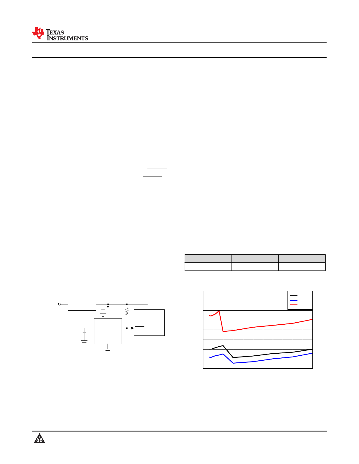
VDD
GND
RESET
Microcontroller
VDD
5 V
RESET
LDO
3.3 V
CT
IN
OUT
*R
pu
*R
pu
only for open-drain output
VDD (V)
I
DD
(µA)
0.5 1 1.5 2 2.5 3 3.5 4 4.5 5 5.5 6
0.08
0.12
0.16
0.2
0.24
0.28
0.32
0.36
0.4
IDDv
25°C
-40°C
125°C
TLV840
www.ti.com
SNVSBC3C – DECEMBER 2019 – REVISED SEPTEMBER 2020
SNVSBC3C – DECEMBER 2019 – REVISED SEPTEMBER 2020
TLV840
TLV840 Nano-Power Ultra-Low Voltage Supervisor with Adjustable Reset Time Delay
1 Features
• Operating voltage range : 0.7 V to 6 V
• Nano supply current : 120 nA (Typical)
• Fixed threshold voltage (V
): 0.8 V to 5.4 V
IT-
– Threshold voltages available in 100mV steps
– High accuracy: ±0.5% (Typical)
– Built-in hysteresis (V
): 5% (Typical)
HYS
• Reset time delay (tD): capacitor-based
programmable (TLV840C, TLV840M)
– Minimum time delay: 40 µs (typical) without
capacitor
• Active-low manual reset (MR) (TLV840M)
• Four output topologies:
– TLV840xxDL: open-drain, active-low (RESET)
– TLV840xxPL: push-pull, active-low (RESET)
– TLV840xxDH: open-drain, active-high (RESET)
– TLV840xxPH: push-pull, active-high (RESET)
• Wide temperature range: –40°C to +125°C
• Package: SOT23-5 (DBV)
2 Applications
• Motor Drives
• Factory Automation and Control
• Home Theater and Entertainment
• Electronic Point of Sale
• Grid Infrastructure
• Data Center and Enterprise Computing
• Multifunction Printer
3 Description
The TLV840 family of voltage supervisors or reset ICs
can operate at high voltage levels while maintaining
very low quiescent current across the whole VDD and
temperature range. TLV840 offers best combination of
low power consumption, high accuracy and low
propagation delay (t
Reset output signal is asserted when the voltage at
VDD drops below the negative voltage threshold
(V
). Reset signal is cleared when VDD rise above
IT-
V
plus hysteresis (V
IT-
(tD) expires. Reset time delay can be programmed by
connecting a capacitor between the CT pin and
ground for TLV840C and TLV840M. For a minimum
reset delay time the CT pin can be left floating.
TLV840N does not offer a programmable delay and
offers fixed reset delay timing options: 40 µs, 2 ms, 10
ms, 30 ms, 50 ms, 80 ms, 100 ms, 150 ms, 200 ms.
Additional features: Low power-on reset voltage
(V
), built-in glitch immunity protection for VDD,
POR
built-in hysteresis, low open-drain output leakage
current (I
). TLV840 is a perfect voltage
lkg(OD)
monitoring solution for industrial applications and
battery-powered / low-power applications.
Device Information
PART NUMBER PACKAGE
TLV840 SOT-23 (5) (DBV) 2.90 mm × 1.60 mm
(1) For package details, see the mechanical drawing addendum
at the end of the data sheet.
= 30 µs typical).
p_HL
) and the reset time delay
HYS
(1)
BODY SIZE (NOM)
Typical Application Circuit
Copyright © 2020 Texas Instruments Incorporated
An IMPORTANT NOTICE at the end of this data sheet addresses availability, warranty, changes, use in safety-critical applications,
intellectual property matters and other important disclaimers. PRODUCTION DATA.
Product Folder Links: TLV840
Typical Supply Current
Submit Document Feedback
1
Page 2

TLV840
SNVSBC3C – DECEMBER 2019 – REVISED SEPTEMBER 2020
www.ti.com
Table of Contents
1 Features............................................................................1
2 Applications..................................................................... 1
3 Description.......................................................................1
4 Revision History.............................................................. 2
5 Device Comparison......................................................... 3
6 Pin Configuration and Functions...................................4
Pin Functions.................................................................... 4
7 Specifications.................................................................. 5
7.1 Absolute Maximum Ratings ....................................... 5
7.2 ESD Ratings .............................................................. 5
7.3 Recommended Operating Conditions ........................5
7.4 Thermal Information ...................................................5
7.5 Electrical Characteristics ............................................6
7.6 Timing Requirements .................................................7
7.7 Timing Diagrams ........................................................8
7.8 Typical Characteristics................................................9
8 Detailed Description......................................................10
8.1 Overview................................................................... 10
8.2 Functional Block Diagram......................................... 10
8.3 Feature Description...................................................10
8.4 Device Functional Modes..........................................14
9 Application and Implementation.................................. 15
9.1 Application Information............................................. 15
9.2 Typical Application.................................................... 15
10 Power Supply Recommendations..............................18
11 Layout...........................................................................19
11.1 Layout Guidelines................................................... 19
11.2 Layout Example...................................................... 19
12 Device and Documentation Support..........................20
12.1 Device Nomenclature..............................................20
12.2 Receiving Notification of Documentation Updates..21
12.3 Support Resources................................................. 21
12.4 Trademarks.............................................................21
13 Mechanical, Packaging, and Orderable
Information.................................................................... 21
4 Revision History
NOTE: Page numbers for previous revisions may differ from page numbers in the current version.
Changes from Revision B (July 2020) to Revision C (September 2020) Page
• Updated the numbering format for tables, figures, and cross-references throughout the document..................1
• Updated Pin Connections................................................................................................................................... 4
• Added Timing Diagram....................................................................................................................................... 8
• New Typical Characteristics................................................................................................................................9
Changes from Revision A (February 2020) to Revision B (July 2020) Page
• APL to RTM release............................................................................................................................................1
Changes from Revision * (December 2019) to Revision A (February 2020) Page
• Initial APL Release............................................................................................................................................. 1
2 Submit Document Feedback
Product Folder Links: TLV840
Copyright © 2020 Texas Instruments Incorporated
Page 3
TLV 840 X X XX XX XXX
Feature Option
N: no capacitor delay (CT),
no manual reset (MR)
C: Capacitor delay (CT)
M: Capacitor delay (CT) and
manual reset (MR)
Output Type
DL: Open-drain,
active-low
PL: Push-pull,
active-low
DH: Open-drain,
active-high
PH: Push-pull,
active-high
Detect Voltage Threshold
08: 0.8V
...
54: 5.4V
Delay Optio n
A: 40 µs
B: 2 ms
C: 10 ms
D: 30 ms
E: 50 ms
F: 80 ms
G: 100 ms
H: 150 ms
I: 200 ms
Package
DBV: SOT23
www.ti.com
SNVSBC3C – DECEMBER 2019 – REVISED SEPTEMBER 2020
5 Device Comparison
Figure 5-1 shows the device naming nomenclature to compare the different device variants. See Table 12-1 for a
more detailed explanation.
Figure 5-1. Device Naming Nomenclature
TLV840
Orderable part numbers starting with TLV840C and TLV840M are only available with the delay option A.
However, longer delays can be achieved through an external capacitor on the CT pin. Leaving the CT pin
floating will result in typical 40us delay for these 2 feature options.
Copyright © 2020 Texas Instruments Incorporated
Product Folder Links: TLV840
Submit Document Feedback
3
Page 4
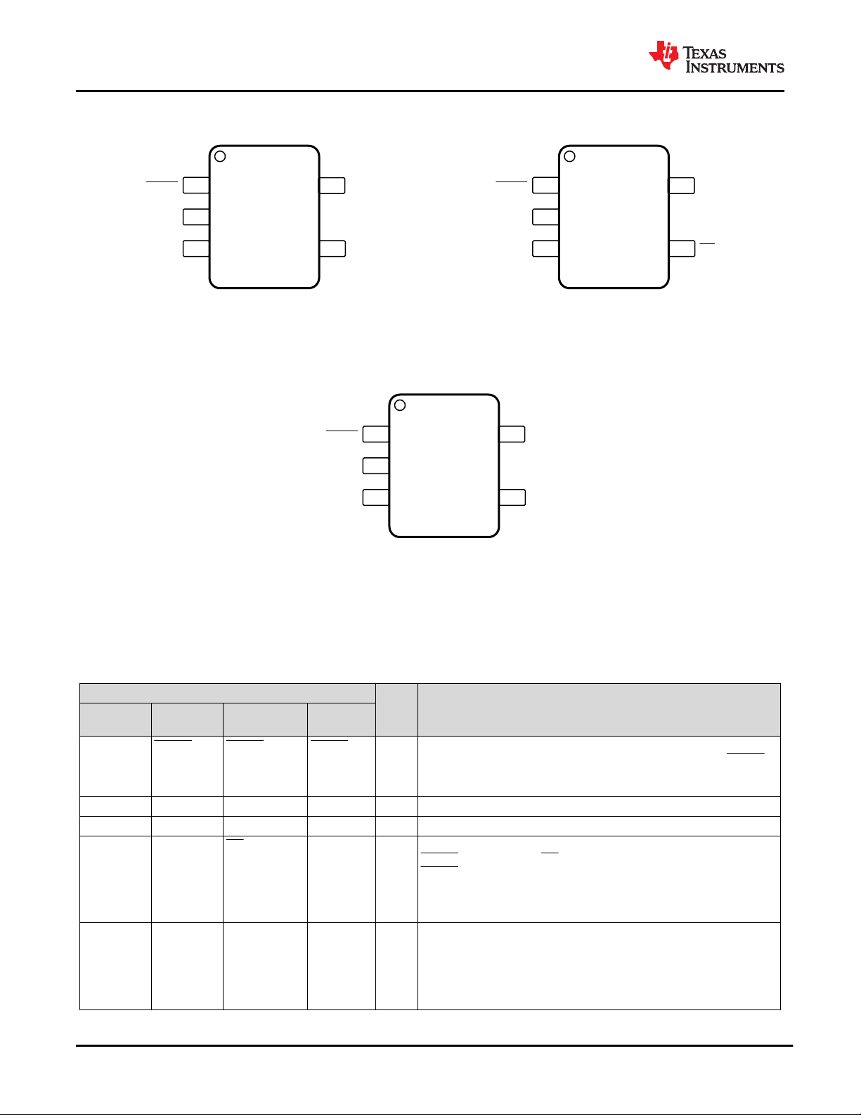
1RESET
2VDD
3GND 4
5
CT
Not to scale
NC
1RESET
2VDD
3GND 4
5
CT
Not to scale
MR
1RESET
2VDD
3GND 4
5 NC
Not to scale
NC
TLV840
SNVSBC3C – DECEMBER 2019 – REVISED SEPTEMBER 2020
6 Pin Configuration and Functions
www.ti.com
Figure 6-1. Pin Configuration TLV840C,
DBV Package, 5-Pin SOT-23,
TLV840C Top View
Figure 6-2. Pin Configuration TLV840M,
DBV Package, 5-Pin SOT-23,
TLV840M Top View
Figure 6-3. Pin Configuration TLV840N,
DBV Package, 5-Pin SOT-23,
TLV840N Top View
Pin Functions
PIN
PIN
TLV840CxL TLV840MxL TLV840NxL
NUMBER
1 RESET RESET RESET O Active-Low Output Reset Signal: This pin is driven logic low when
2 VDD VDD VDD I Input Supply Voltage TLV840 monitors VDD voltage
3 GND GND GND _ Ground
4 NC MR NC I Manual Reset Pull this pin to a logic low to assert a reset signal in the
5 CT CT NC - Capacitor Time Delay Pin. The CT pin offers a user-programmable
I/O DESCRIPTION
VDD voltage falls below the negative voltage threshold (V
remains low (asserted) for the delay time period (tD) after VDD voltage
rises above V
IT+=VIT-+VHYS
.
RESET output pin. After MR pin is left floating or pulls to logic high, the
RESET output deasserts to the nominal state after the reset delay time
(tD)expires.
NC stands for “No Connect”. The pin can be left floating.
Recommended connection to GND.
delay time. Connect an external capacitor on this pin to adjust time
delay. When not in use leave pin floating for the smallest fixed time
delay.
NC stands for “No Connect”. The pin can be left floating.
Recommended connection to GND.
). RESET
IT-
4 Submit Document Feedback
Copyright © 2020 Texas Instruments Incorporated
Product Folder Links: TLV840
Page 5
www.ti.com
SNVSBC3C – DECEMBER 2019 – REVISED SEPTEMBER 2020
7 Specifications
TLV840
7.1 Absolute Maximum Ratings
over operating free-air temperature range, unless otherwise noted
Voltage VDD –0.3 6.5 V
Voltage
CT, MR
RESET (TLV840xxDL) –0.3 6.5
Current RESET, RESET pin –20 20 mA
Temperature
Temperature
(4)
(4)
Operating ambient temperature, T
Storage, T
(1) Stresses beyond those listed under Absolute Maximum Rating may cause permanent damage to the device. These are stress ratings
only, which do not imply functional operation of the device at these or any other conditions beyond those indicated under
Recommended Operating Condition. Exposure to absolute-maximum-rated conditions for extended periods may affect device
reliability.
(2) If the logic signal driving
MR is less than VDD, then additional current flows into VDD and out of MR.
(3) The absolute maximum rating is (VDD + 0.3) V or 6.5 V, whichever is smaller
(4) As a result of the low dissipated power in this device, it is assumed that TJ = TA.
(2)
, RESET (TLV840xxPL) –0.3 VDD+0.3
A
stg
7.2 ESD Ratings
Human body model (HBM), per ANSI/ESDA/JEDEC
(1)
V
(ESD)
Electrostatic discharge
JS-001
Charged device model (CDM), per JEDEC specification
JESD22-C101
(2)
(1)
MIN MAX UNIT
(3)
V
–40 125
–65 150
℃
VALUE UNIT
± 2000
V
± 750
(1) JEDEC document JEP155 states that 500-V HBM allows safe manufacturing with a standard ESD control process.
(2) JEDEC document JEP157 states that 250-V CDM allows safe manufacturing with a standard ESD control process.
7.3 Recommended Operating Conditions
over operating free-air temperature range (unless otherwise noted)
MIN NOM MAX UNIT
Voltage
Current RESET pin current –5 5 mA
T
A
VDD (TLV840xxxL) 0.7 6
CT, RESET (TLV840xxxL), MR 0 6
Operating ambient temperature –40 125 ℃
V
7.4 Thermal Information
TLV840
THERMAL METRIC
R
θJA
R
θJC(top)
R
θJB
ψ
JT
ψ
JB
R
θJC(bot)
Junction-to-ambient thermal resistance 193.5 °C/W
Junction-to-case (top) thermal resistance 117.9 °C/W
Junction-to-board thermal resistance 98.5 °C/W
Junction-to-top characterization parameter 43.4 °C/W
Junction-to-board characterization parameter 97.8 °C/W
Junction-to-case (bottom) thermal resistance N/A °C/W
(1) For more information about traditional and new thermal metrics, see the Semiconductor and IC Package Thermal Metrics application
report.
(1)
UNITDBV (SOT23-5)
5 PINS
Copyright © 2020 Texas Instruments Incorporated
Product Folder Links: TLV840
Submit Document Feedback
5
Page 6
TLV840
SNVSBC3C – DECEMBER 2019 – REVISED SEPTEMBER 2020
7.5 Electrical Characteristics
At 0.7 V ≤ VDD ≤ 6 V, CT = MR = Open, RESET pull-up resistor (R
load (C
VDD ramp rate ≤ 100 mV/µs. Typical values are at TA = 25℃
COMMON PARAMETERS
V
DD
V
IT–
V
HYS
I
DD
V
MR_L
V
MR_H
R
MR
R
CT
TLV840xxDL (Open-drain active-low)
V
POR
V
OL
I
lkg(OD)
TLV840xxPL (Push-pull active-low)
V
POR
V
OL
V
OH
) = 10 pF and over operating free-air temperature range –40℃ to 125℃, unless otherwise noted.
LOAD
PARAMETER TEST CONDITIONS MIN TYP MAX UNIT
Input supply voltage TLV840xxxL 0.7 6 V
V
= 0.8 V to 1.7 V –2.5 ±0.5 2.5
Negative-going input threshold accuracy
(1)
Hysteresis on V
pin 2.5 5 7 %
IT–
IT-
V
= 1.8 V to 5.4 V –2 ±0.5 2
IT-
VDD = 2 V
V
= 0.8 V to 1.8 V
IT–
Supply current into VDD pin
(2)
VDD = 6 V
V
= 0.8 V to 5.5 V
IT–
Manual reset logic low input
Manual reset logic high input
(2)
(2)
Manual reset internal pull-up resistance 100 kΩ
CT pin internal resistance 500 kΩ
V
= 300 mV
Power on Reset Voltage
(3)
Low level output voltage
Open-Drain output leakage current
Power on Reset Voltage
(3)
Low level output voltage
High level output voltage
OL(max)
I
OUT(Sink)
= 15 µA
VDD = 0.7 V, 0.8 V ≤ V
I
OUT(Sink)
= 15 µA
VDD =1.5 V, 1.6 V ≤ V
I
OUT(Sink)
= 500 µA
VDD = 3.3 V, 3.4 V ≤ V
I
VDD = V
OUT(Sink)
= 2 mA
PULLUP
= 6V
TA = –40℃ to 85℃
VDD = V
V
OL(max)
I
OUT(Sink)
= 6V 10 350 nA
PULLUP
= 300 mV
= 15 µA
VDD = 0.7 V, 0.8 V ≤ V
I
OUT(Sink)
= 15 µA
VDD = 1.5 V, 1.6 V ≤ V
I
OUT(Sink)
= 500 µA
VDD = 3.3 V, 3.4 V ≤ V
I
V
I
V
I
V
I
= 2 mA
OUT(Sink)
= 1.8 V, 0.8 V ≤ V
DD
OUT(Source)
DD
OUT(Source)
DD
OUT(Source)
= 500 µA
= 3.3 V, 1.5 V ≤ V
= 500 µA
= 6 V, 3.1 V ≤ V
= 2 mA
IT–
IT–
IT–
IT–
IT–
IT–
IT–
IT–
≤ 5.5 V
IT–
) = 100 kΩ to VDD, output reset
pull-up
TA = –40℃ to
85℃
TA = –40℃ to
85℃
≤ 1.5 V
≤ 3.3 V
≤ 5.5 V
≤ 1.5 V
≤ 3.3 V
≤ 5.5 V
≤ 1.4 V
≤ 3.0 V
0.7V
0.8V
0.8V
0.8V
DD
DD
DD
DD
www.ti.com
0.12 0.3
0.12 1.0
0.15 0.4
0.15 1.2
0.3V
DD
700 mV
300
300
300
10 100 nA
700 mV
300
300
300
%
µA
V
V
mV
mV
V
(1) V
threshold voltage range from 0.8 V to 5.4 V (for DL, PL versions) in 100 mV steps
IT–
(2) If the logic signal driving MR is less than VDD, then I
(3) V
is the minimum VDD voltage level for a controlled output state
POR
6 Submit Document Feedback
current increases based on voltage differential
DD
Product Folder Links: TLV840
Copyright © 2020 Texas Instruments Incorporated
Page 7
www.ti.com
7.6 Timing Requirements
At 0.7 V ≤ VDD ≤ 6 V, CT = MR = Open, RESET pull-up resistor (R
load (C
VDD ramp rate ≤ 100 mV/µs. Typical values are at TA = 25℃
t
P_HL
t
D
t
GI_VIT–
t
MR_PW
t
MR_RES
t
MR_tD
) = 10 pF and over operating free-air temperature range –40℃ to 125℃, unless otherwise noted.
LOAD
PARAMETER TEST CONDITIONS MIN TYP MAX UNIT
Propagation detect delay for VDD falling
below V
IT–
TLV840xA
Reset time delay
TLV840CA,
TLV840MA
Glitch immunity V
MR pin pulse duration to assert reset
IT–
(3)
Propagation delay from MR low to reset
assertion
Delay from MR release to reset deassert
V
: (V
DD
(1)
+ 10%) to (V
IT+
CT pin = Open or NC
(V
- 10%) to (V
IT-
IT+
CT pin = 10 nF 6.2 ms
CT pin = 1 µF 619 ms
5% V
overdrive
IT–
(2)
VDD = 3.3 V,
MR = V
MR_H
to V
MR_L
VDD = 3.3 V,
MR = V
MR_L
to V
MR_H
SNVSBC3C – DECEMBER 2019 – REVISED SEPTEMBER 2020
) = 100 kΩ to VDD, output reset
pull-up
– 10%)
IT–
+ 10%)
30 50 µs
40 80 µs
10 µs
500 ns
1 µs
t
D
TLV840
ms
(1) t
(2) Overdrive % = [(VDD/ V
measured from threshold trip point (V
P_HL
) – 1] × 100%
IT–
) to RESET assert. V
IT–
(3) Refer section on Manual Reset Input for min pulse width needed on
= V
IT+
MR pin
IT–
+ V
HYS
Copyright © 2020 Texas Instruments Incorporated
Product Folder Links: TLV840
Submit Document Feedback
7
Page 8
t
D
t
P_HL
VDD
V
POR
V
OH
V
OL
V
IT+
V
IT-
RESET
t
P_HL
V
DD(0v)
tD
t
D
t
D
t
P_HL
VDD
V
POR
V
OH
V
OL
V
IT+
V
IT-
RESET
t
P_HL
t
D
t
D
TLV840
SNVSBC3C – DECEMBER 2019 – REVISED SEPTEMBER 2020
7.7 Timing Diagrams
www.ti.com
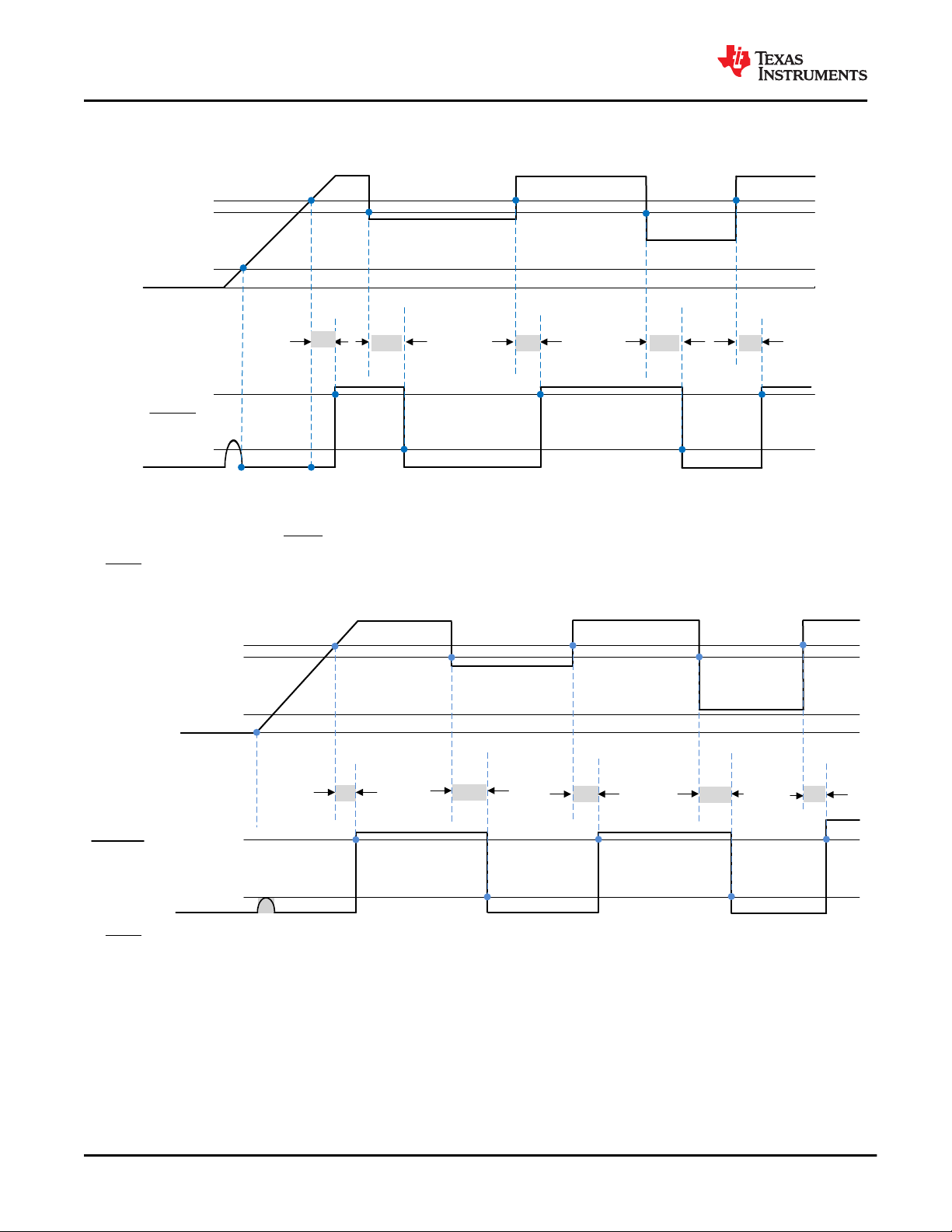
(1) Open-Drain timing diagram where RESET is pulled up to VDD via a pull-up resistor
(2) RESET output is undefined when VDD is < V
POR
Figure 7-1. Timing Diagram TLV840DL (Open-Drain Active-Low)
(3) RESET output is undefined when VDD is < V
Figure 7-2. Timing Diagram TLV840PL (Push-Pull Active-Low)
and limited to VOL for VDD slew rate = 100mV / μS
POR
8 Submit Document Feedback
Copyright © 2020 Texas Instruments Incorporated
Product Folder Links: TLV840
Page 9
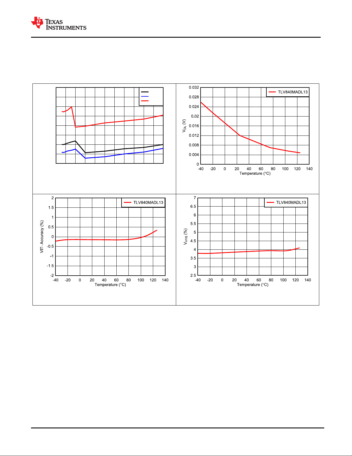
VDD (V)
I
DD
(µA)
0.5 1 1.5 2 2.5 3 3.5 4 4.5 5 5.5 6
0.08
0.12
0.16
0.2
0.24
0.28
0.32
0.36
0.4
IDDv
25°C
-40°C
125°C
www.ti.com
SNVSBC3C – DECEMBER 2019 – REVISED SEPTEMBER 2020
7.8 Typical Characteristics
Typical characteristics show the typical performance of the TLV840 device. Test conditions are TA = 25°C,
TLV840
VDD = 3.3 V, R
Pull-Up
= 100 kΩ, C
= 50 pF, unless otherwise noted.
LOAD
Figure 7-3. Supply Current vs Supply Voltage for
TLV840MADL13
Figure 7-4. Low Output Voltage (VOL) vs
Temperature for TLV840MADL13 (VDD = 0.7 V)
Figure 7-5. Voltage Threshold Accuracy vs
Temperature for TLV840MADL13
Copyright © 2020 Texas Instruments Incorporated
Figure 7-6. Voltage Hysteresis vs Temperature for
Product Folder Links: TLV840
TLV840MADL13
Submit Document Feedback
9
Page 10

+
±
Ref erence
GND
VDD
RESET
GND
VDD
RESET
LOGIC
TIMER
CT
Push-pull (TLV840xxxPx)
version only
R
CT
TLV840C,
TLV840M
only
R
MR
VDD
TLV840M
only
MR
TLV840
SNVSBC3C – DECEMBER 2019 – REVISED SEPTEMBER 2020
www.ti.com
8 Detailed Description
8.1 Overview
The TLV840 is a family of nano-quiescent current voltage detectors with fixed threshold voltage. TLV840
features include programable reset time delay using external capacitor, active-low manual reset, 0.5% typical
monitor threshold accuracy with hysteresis and glitch immunity.
Fixed negative threshold voltages (V
) can be factory set from 0.8 V to 5.4 V. TLV840 is available in
IT-
SOT-23 5-pin industry standard package.
8.2 Functional Block Diagram
8.3 Feature Description
8.3.1 Input Voltage (VDD)
VDD pin is monitored by the internal comparator to indicate when VDD falls below the fixed threshold voltage.
VDD also functions as the supply for the internal bandgap, internal regulator, state machine, buffers and other
control logic blocks. Good design practice involve placing a 0.1 μF to 1 μF bypass capacitor at VDD input for
noisy applications to ensure enough charge is available for the device to power up correctly.
10 Submit Document Feedback
Product Folder Links: TLV840
Copyright © 2020 Texas Instruments Incorporated
Page 11

Hystersis Width
V
IT+
V
IT-
RESET
RESET
Hystersis Width
V
IT+
V
IT-
Overdrive
Pulse
Duration
VDD
V
IT-
V
IT+
www.ti.com
SNVSBC3C – DECEMBER 2019 – REVISED SEPTEMBER 2020
8.3.1.1 VDD Hysteresis
The internal comparator has built-in hysteresis to avoid erroneous output reset release. If the voltage at the VDD
TLV840
pin falls below V
(V
) the output reset is deasserted after tD delay.
HYS
the output reset is asserted. When the voltage at the VDD pin goes above V
IT-
plus hysteresis
IT-
Figure 8-1. Hysteresis Diagram
8.3.1.2 VDD Transient Immunity
The TLV840 is immune to quick voltage transients or excursion on VDD. Sensitivity to transients depends on
both pulse duration (t
) found in Section 7.6 and overdrive. Overdrive is defined by how much VDD deviates
GI_VIT-
from the specified threshold. Threshold overdrive is calculated as a percent of the threshold in question, as
shown in Equation 1.
Overdrive = | (V
DD
/ V
– 1) × 100% |
IT-
(1)
Figure 8-2. Overdrive vs Pulse Duration
Copyright © 2020 Texas Instruments Incorporated
Product Folder Links: TLV840
Submit Document Feedback
11
Page 12

VDD Fault Underoltage (V)
Fault Time to Reset Delay Time Ratio (%)
0.6 0.8 1 1.2 1.4 1.6 1.8 2
5
10
15
20
25
30
35
40
45
50
55
CTR_
25°C
TLV840
SNVSBC3C – DECEMBER 2019 – REVISED SEPTEMBER 2020
www.ti.com
8.3.2 User-Programmable Reset Time Delay
The reset time delay can be set to a minimum value of 80 µs by leaving the CT pin floating, or a maximum value
of approximately 6.2 seconds by connecting 10 µF delay capacitor. The reset time delay (tD) can be
programmed by connecting a capacitor no larger than 10 µF between CT pin and GND.
The relationship between external capacitor (CCT) in µF at CT pin and the time delay (tD) in seconds is given by
Equation 2.
tD = -ln (0.29) x RCT x CCT + tD (CT pin = Open)
(2)
Equation 2 is simplified to Equation 3 by plugging RCT and tD (CT pin = Open) given in Section 7.5 section:
tD = 618937 x CCT + 80µs
(3)
Equation 4 solves for external capacitor value (CCT) in units of µF where tD is in units of seconds
C
= (tD- 80µs) ÷ 618937
CT
(4)
The recommended maximum delay capacitor for the TLV840 is limited to 10 µF as this ensures there is enough
time for the capacitor to fully discharge when the reset condition occurs. When a voltage fault occurs, the
previously charged up capacitor discharges, and if the monitored voltage returns from the fault condition before
the delay capacitor discharges completely, the reset delay will be shorter than expected because the delay
capacitor will begin charging from a voltage above zero. Larger delay capacitors can be used so long as the
capacitor has enough time to fully discharge during the duration of the voltage fault. The amount of time required
to discharge the delay capacitor relative to the reset delay increases as VDD overdrive increases as shown in
Figure 8-3.
Figure 8-3. CCT Discharge Time During Fault Condition (V
12 Submit Document Feedback
Product Folder Links: TLV840
= 2.1 V, CCT = 1 µF)
IT-
Copyright © 2020 Texas Instruments Incorporated
Page 13

V
IT+
t
P_HL
V
HYS
V
IT-
t
D
V
IT+
V
HYS
V
IT-
t
MR_tD
V
MR_L
Time
t
MR_RES
t
MR_PW
(1)
MR
VDD
RESET
V
MR_H
(2)
(1) MR pulse width too small to assert RESET
(2) MR voltage not low enough to assert RESET
www.ti.com
SNVSBC3C – DECEMBER 2019 – REVISED SEPTEMBER 2020
8.3.3 Manual Reset (MR) Input for TLV840M Only
The manual reset (MR) input allows a processor GPIO or other logic circuits to initiate a reset. A logic low on MR
TLV840
with pulse duration longer than t
(V
) and VDD is above V
MR_H
MR_PW
, reset is deasserted after the user programmed reset time delay (tD) expires.
IT+
The minimum duration for which MR is held under V
reset delay will be shorter roughly by the difference between 1% of t
will cause the reset output to assert. After MR returns to a logic high
must be at least 1% of t
MR_L
MR_tD
and the actual MR pulse width. For
. Otherwise, the effective
MR_tD
large capacitor based delays this difference could be noticeable unless care is taken to lengthen the MR pulse
width.
MR is internally connected to VDD through a pull-up resistor R
shown in Section 8.2. If the logic signal
MR
controlling MR is less than VDD, then additional current flows from VDD into MR internally. For minimum current
consumption, drive MR to either VDD or GND. V
should not be higher than VDD voltage.
MR
Figure 8-4. Timing Diagram MR and RESET (TLV840M)
Copyright © 2020 Texas Instruments Incorporated
Product Folder Links: TLV840
Submit Document Feedback
13
Page 14

TLV840
SNVSBC3C – DECEMBER 2019 – REVISED SEPTEMBER 2020
www.ti.com
8.3.4 Output Logic
8.3.4.1 RESET Output, Active-Low
RESET (Active-Low) applies to TLV840DL (Open-Drain) and TLV840PL (Push-Pull) hence the "L" in the device
name. RESET remains high (deasserted) as long as VDD is above the negative threshold (V
floating or above V
. If VDD falls below the negative threshold (V
MR_H
) or if MR is driven low, then RESET is
IT-
) and the MR pin is
IT-
asserted.
When MR is again logic high or floating and VDD rise above V
, the delay circuit will hold RESET low for the
IT+
specified reset time delay (tD). When the reset time delay has elapsed, the RESET pin goes back to logic high
voltage (VOH).
The TLV840DL (Open-Drain) version, denoted with "D" in the device name, requires a pull-up resistor to hold
RESET pin high. Connect the pull-up resistor to the desired pull-up voltage source and RESET can be pulled up
to any voltage up to 6.5 V independent of the VDD voltage. To ensure proper voltage levels, give some
consideration when choosing the pull-up resistor values. The pull-up resistor value determines the actual VOL,
the output capacitive loading, and the output leakage current (I
lkg(OD)
).
The Push-Pull variants (TLV840PL and TLV840PH), denoted with "P" in the device name, does not require an
external pull-up resistor.
8.4 Device Functional Modes
Table 8-1 summarizes the various functional modes of the device. Logic high is represented by "H" and logic low
is represented by "L".
Table 8-1. Truth Table
VDD MR RESET RESET
VDD < V
V
POR
VDD ≥ V
VDD ≥ V
VDD ≥ V
POR
< VDD < V
IT-
IT-
IT-
IT-
Ignored Undefined Undefined
Ignored H L
L H L
H L H
Floating L H
8.4.1 Normal Operation (VDD > VPOR)
When VDD is greater than VPOR, the reset signal is determined by the voltage on the VDD pin with respect to
the trip point (V
IT-
)
• MR high: the reset signal corresponds to VDD with respect to the threshold voltage.
• MR low: in this mode, the reset is asserted regardless of the threshold voltage.
8.4.2 Below Power-On-Reset (VDD < V
When the voltage on VDD is lower than V
)
POR
, the device does not have enough bias voltage to internally pull the
POR
asserted output low or high and reset voltage level is undefined.
14 Submit Document Feedback
Product Folder Links: TLV840
Copyright © 2020 Texas Instruments Incorporated
Page 15

TLV840CAPL29
VDD
GNDCT
RESET
TLV840CADL09
VDD
GND
RESET
CT
Microcontroller
V
CORE
3.3 V
RESET
VDD
LDO
EN
1.2 V
0.047µF
VI/O
NC
1 µF 1 µF
40kŸ
www.ti.com
SNVSBC3C – DECEMBER 2019 – REVISED SEPTEMBER 2020
9 Application and Implementation
Note
Information in the following applications sections is not part of the TI component specification, and TI
does not warrant its accuracy or completeness. TI’s customers are responsible for determining
suitability of components for their purposes. Customers should validate and test their design
implementation to confirm system functionality.
9.1 Application Information
The following sections describe in detail how to properly use this device, depending on the requirements of the
final application.
9.2 Typical Application
9.2.1 Design 1: Dual Rail Monitoring with Power-up Sequencing
A typical application for the TLV840 is voltage rail monitoring and power-up sequencing as shown in Figure 9-1.
The TLV840 can be used to monitor any rail above 0.9 V. In this design application, two TLV840 devices monitor
two separate voltage rails and sequences the rails upon power-up. The TLV840CAPL29 is used to monitor the
3.3-V main power rail and the TLV840CADL09 is used to monitor the 1.2-V rail provided by the LDO for other
TLV840
system peripherals. The
reset event is initiated on either voltage supervisor when the VDD voltage is less than V
RESET output of the TLV840CAPL29 is connected to the ENABLE input of the LDO. A
.
IT-
Copyright © 2020 Texas Instruments Incorporated
Figure 9-1. TLV840 Voltage Rail Monitor and Power-Up Sequencer Design Block Diagram
Product Folder Links: TLV840
Submit Document Feedback
15
Page 16

VDD
RESET
(LDO Enable)
V (LDO)
OUT
30ms delay from VDD (3.3 V) to LDO Enable set by 0.047 µF on CT of TLV840CAPL29
Negligible delay from LDO Enable to 1.2 V V
OUT
TLV840
SNVSBC3C – DECEMBER 2019 – REVISED SEPTEMBER 2020
www.ti.com
9.2.1.1 Design Requirements
This design requires voltage supervision on two separate rails: 3.3-V and 1.2-V rails. The voltage rail needs to
sequence upon power up with the 3.3-V rail coming up first followed by the 1.2-V rail at least 25 ms after.
PARAMETER DESIGN REQUIREMENT DESIGN RESULT
Two Rail Voltage Supervision Monitor 3.3-V and 1.2-V rails
Voltage Rail Sequencing
Maximum device current
consumption
Power up the 3.3-V rail first followed by 1.2-V rail
25 ms after
1 µA Each TLV840 requires 350 nA typical
Two TLV840 devices provide voltage monitoring
with 1% accuracy with device options available in
0.1 V variations
The CT capacitor on TLV840CAPL29 is set to
0.047 µF for a reset time delay of 29 ms typical
9.2.1.2 Detailed Design Procedure
The primary constraint for this application is choosing the correct device to monitor the supply voltage of the
microprocessor. The TLV840 can monitor any voltage between 0.8 V and 5.4 V. Depending on how far away
from the nominal voltage rail the user wants the voltage supervisor to trigger determines the correct voltage
supervisor variant to choose. In this example, the first TLV840 triggers when the 3.3-V rail falls to 2.9 V. The
second TLV840 triggers a reset when the 1.2-V rail falls to 0.9 V. The secondary constraint for this application is
the reset time delay that must be at least 25 ms to allow the microprocessor, and all other devices using the
3.3-V rail, enough time to startup correctly before the 1.2-V rail is enabled via the LDO. Because a minimum time
is required, the user must account for capacitor tolerance. For applications with ambient temperatures ranging
from –40°C to +125°C, CCT can be calculated using RCT and solving for CCT in Equation 2. Solving Equation 2
for 25 ms gives a minimum capacitor value of 0.04 µF which is rounded up to a standard value 0.047 µF to
account for capacitor tolerance.
A 1 µF decoupling capacitor is connected to the VDD pin as a good analog design practice. The pull-up resistor
is only required for the Open-Drain device variants and is calculated to ensure that VOL does not exceed max
limit given the Isink possible at the expected supply voltage. In this design example nominal VDD is 1.2 V but
dropping to 0.9 V. The Recommended Operating Conditions table provides 15 µA I sink for 0.7 V VDD, which is
the closest voltage to this design example. Using 15 µA of Isink and 300 mV max VOL, gives us 40 kΩ for the
pull-up resistor. Any value higher than 40 kΩ would ensure that VOL will not exceed 300 mV max specification.
9.2.1.3 Application Curves
Figure 9-2. Startup Sequence Highlighting the Delay Between 3.3V and 1.2V Rails
16 Submit Document Feedback
Product Folder Links: TLV840
Copyright © 2020 Texas Instruments Incorporated
Page 17

VDD
RESET
Reset Delay (tD)= 57.6 µs
VDD
RESET
Reset Delay (tD)= 5.42 ms
VDD
RESET
Reset Delay (tD)= 56.8 ms
www.ti.com
SNVSBC3C – DECEMBER 2019 – REVISED SEPTEMBER 2020
9.2.2 Application Curve: TLV840EVM
These application curves are taken with the TLV840EVM. Please see the TLV840EVM User Guide for more
information.
TLV840
Figure 9-3. TLV840EVM RESET Time Delay (tD) with
No Capacitor
Figure 9-5. TLV840EVM RESET Time Delay (tD) with 0.1-µF Capacitor
Figure 9-4. TLV840EVM RESET Time Delay (tD) with
0.01-µF Capacitor
Copyright © 2020 Texas Instruments Incorporated
Product Folder Links: TLV840
Submit Document Feedback
17
Page 18

TLV840
SNVSBC3C – DECEMBER 2019 – REVISED SEPTEMBER 2020
www.ti.com
10 Power Supply Recommendations
These devices are designed to operate from an input supply with a voltage range between 0.7 V and 6 V. TI
recommends an input supply capacitor between the VDD pin and GND pin. This device has a 6.5 V absolute
maximum rating on the VDD pin. If the voltage supply providing power to VDD is susceptible to any large voltage
transient that can exceed 6.5 V, additional precautions must be taken.
18 Submit Document Feedback
Copyright © 2020 Texas Instruments Incorporated
Product Folder Links: TLV840
Page 19

GND
C
IN
GND
VDD
C
CT
R
pull-up
RESET
CT
NC
VDD
Pull-up resistor required for Open-Drain
(TLV840XXDX) only
www.ti.com
SNVSBC3C – DECEMBER 2019 – REVISED SEPTEMBER 2020
11 Layout
11.1 Layout Guidelines
Make sure that the connection to the VDD pin is low impedance. Good analog design practice recommends
placing a minimum 0.1 µF ceramic capacitor as near as possible to the VDD pin. If a capacitor is not connected
to the CT pin, then minimize parasitic capacitance on this pin so the rest time delay is not adversely affected.
• Make sure that the connection to the VDD pin is low impedance. Good analog design practice is to place a
>0.1 µF ceramic capacitor as near as possible to the VDD pin.
• If a CCT capacitor is used, place these components as close as possible to the CT pin. If the CT pin is left
unconnected, make sure to minimize the amount of parasitic capacitance on the pin to <5 pF.
TLV840
• Place the pull-up resistors on
11.2 Layout Example
The layout example in shows how the TLV840 is laid out on a printed circuit board (PCB) with a user-defined
delay.
RESET pin as close to the pin as possible.
Copyright © 2020 Texas Instruments Incorporated
Figure 11-1. TLV840C Recommended Layout
Product Folder Links: TLV840
Submit Document Feedback
19
Page 20

TLV840
SNVSBC3C – DECEMBER 2019 – REVISED SEPTEMBER 2020
www.ti.com
12 Device and Documentation Support
12.1 Device Nomenclature
Table 12-1 shows how to decode the function of the device based on its part number
Table 12-1. Device Naming Convention
DESCRIPTION NOMENCLATURE VALUE
Generic Part number TLV840 TLV840
Feature Option N No capacitor adjustable delay or manual
1
C
1
M
Delay Option A 40 µs (No internal reset time delay)
B 2 ms reset time delay
C 10 ms reset time delay
D 30 ms reset time delay
E 50 ms reset time delay
F 80 ms reset time delay
G 100 ms reset time delay
H 150 ms reset time delay
I 200 ms reset time delay
Variant code (Output Topology) DL Open-Drain, Active-Low
PL Push-Pull, Active-Low
DH Open-Drain, Active-High
PH Push-Pull, Active-High
Detect Voltage Option ## (two characters) Example: 12 stands for 1.2 V threshold
Package DBV SOT23-5
Reel R Large Reel
reset options
CT pin for programmable delay using
external capacitor
Manual Reset option in addition to CT pin
1. Orderable part numbers starting with TLV840C and TLV840M are only available with the delay option A.
However, longer delays can be achieved through an external capacitor on the CT pin. Leaving the CT pin
floating will result in typical 40us delay for these 2 feature options
20 Submit Document Feedback
Product Folder Links: TLV840
Copyright © 2020 Texas Instruments Incorporated
Page 21

www.ti.com
SNVSBC3C – DECEMBER 2019 – REVISED SEPTEMBER 2020
TLV840
12.2 Receiving Notification of Documentation Updates
To receive notification of documentation updates, navigate to the device product folder on ti.com. In the upper
right corner, click on Alert me to register and receive a weekly digest of any product information that has
changed. For change details, review the revision history included in any revised document.
12.3 Support Resources
12.4 Trademarks
All other trademarks are the property of their respective owners.
13 Mechanical, Packaging, and Orderable Information
The following pages include mechanical, packaging, and orderable information. This information is the most
current data available for the designated devices. This data is subject to change without notice and revision of
this document. For browser-based versions of this data sheet, refer to the left-hand navigation.
Copyright © 2020 Texas Instruments Incorporated
Product Folder Links: TLV840
Submit Document Feedback
21
Page 22

PACKAGE OPTION ADDENDUM
www.ti.com
PACKAGING INFORMATION
Orderable Device Status
TLV840CADL11DBVR ACTIVE SOT-23 DBV 5 3000 RoHS & Green NIPDAU Level-1-260C-UNLIM -40 to 125 2CLF
TLV840CADL14DBVR ACTIVE SOT-23 DBV 5 3000 RoHS & Green NIPDAU Level-1-260C-UNLIM -40 to 125 2G1F
TLV840CADL28DBVR ACTIVE SOT-23 DBV 5 3000 RoHS & Green NIPDAU Level-1-260C-UNLIM -40 to 125 2CKF
TLV840CADL29DBVR ACTIVE SOT-23 DBV 5 3000 RoHS & Green NIPDAU Level-1-260C-UNLIM -40 to 125 2CNF
TLV840CADL40DBVR ACTIVE SOT-23 DBV 5 3000 RoHS & Green NIPDAU Level-1-260C-UNLIM -40 to 125 2ILF
TLV840MADL10DBVR ACTIVE SOT-23 DBV 5 3000 RoHS & Green NIPDAU Level-1-260C-UNLIM -40 to 125 2G2F
TLV840MADL13DBVR ACTIVE SOT-23 DBV 5 3000 RoHS & Green NIPDAU Level-1-260C-UNLIM -40 to 125 2CMF
TLV840MADL29DBVR ACTIVE SOT-23 DBV 5 3000 RoHS & Green NIPDAU Level-1-260C-UNLIM -40 to 125 2G3F
TLV840MADL30DBVR ACTIVE SOT-23 DBV 5 3000 RoHS & Green NIPDAU Level-1-260C-UNLIM -40 to 125 2G4F
TLV840NADL20DBVR ACTIVE SOT-23 DBV 5 3000 RoHS & Green NIPDAU Level-1-260C-UNLIM -40 to 125 2G6F
Package Type Package
(1)
Drawing
Pins Package
Qty
Eco Plan
(2)
Lead finish/
Ball material
(6)
MSL Peak Temp
(3)
Op Temp (°C) Device Marking
7-Apr-2021
Samples
(4/5)
TLV840NADL33DBVR ACTIVE SOT-23 DBV 5 3000 RoHS & Green NIPDAU Level-1-260C-UNLIM -40 to 125 2CIF
TLV840NADL35DBVR ACTIVE SOT-23 DBV 5 3000 RoHS & Green NIPDAU Level-1-260C-UNLIM -40 to 125 2CJF
TLV840NADL46DBVR ACTIVE SOT-23 DBV 5 3000 RoHS & Green NIPDAU Level-1-260C-UNLIM -40 to 125 2G7F
TLV840NAPL50DBVR ACTIVE SOT-23 DBV 5 3000 RoHS & Green NIPDAU Level-1-260C-UNLIM -40 to 125 2GOF
(1)
The marketing status values are defined as follows:
ACTIVE: Product device recommended for new designs.
LIFEBUY: TI has announced that the device will be discontinued, and a lifetime-buy period is in effect.
NRND: Not recommended for new designs. Device is in production to support existing customers, but TI does not recommend using this part in a new design.
PREVIEW: Device has been announced but is not in production. Samples may or may not be available.
OBSOLETE: TI has discontinued the production of the device.
(2)
RoHS: TI defines "RoHS" to mean semiconductor products that are compliant with the current EU RoHS requirements for all 10 RoHS substances, including the requirement that RoHS substance
do not exceed 0.1% by weight in homogeneous materials. Where designed to be soldered at high temperatures, "RoHS" products are suitable for use in specified lead-free processes. TI may
reference these types of products as "Pb-Free".
Addendum-Page 1
Page 23

PACKAGE OPTION ADDENDUM
www.ti.com
RoHS Exempt: TI defines "RoHS Exempt" to mean products that contain lead but are compliant with EU RoHS pursuant to a specific EU RoHS exemption.
Green: TI defines "Green" to mean the content of Chlorine (Cl) and Bromine (Br) based flame retardants meet JS709B low halogen requirements of <=1000ppm threshold. Antimony trioxide based
flame retardants must also meet the <=1000ppm threshold requirement.
(3)
MSL, Peak Temp. - The Moisture Sensitivity Level rating according to the JEDEC industry standard classifications, and peak solder temperature.
(4)
There may be additional marking, which relates to the logo, the lot trace code information, or the environmental category on the device.
(5)
Multiple Device Markings will be inside parentheses. Only one Device Marking contained in parentheses and separated by a "~" will appear on a device. If a line is indented then it is a continuation
of the previous line and the two combined represent the entire Device Marking for that device.
(6)
Lead finish/Ball material - Orderable Devices may have multiple material finish options. Finish options are separated by a vertical ruled line. Lead finish/Ball material values may wrap to two
lines if the finish value exceeds the maximum column width.
Important Information and Disclaimer:The information provided on this page represents TI's knowledge and belief as of the date that it is provided. TI bases its knowledge and belief on information
provided by third parties, and makes no representation or warranty as to the accuracy of such information. Efforts are underway to better integrate information from third parties. TI has taken and
continues to take reasonable steps to provide representative and accurate information but may not have conducted destructive testing or chemical analysis on incoming materials and chemicals.
TI and TI suppliers consider certain information to be proprietary, and thus CAS numbers and other limited information may not be available for release.
In no event shall TI's liability arising out of such information exceed the total purchase price of the TI part(s) at issue in this document sold by TI to Customer on an annual basis.
OTHER QUALIFIED VERSIONS OF TLV840 :
Automotive : TLV840-Q1
•
7-Apr-2021
NOTE: Qualified Version Definitions:
Automotive - Q100 devices qualified for high-reliability automotive applications targeting zero defects
•
Addendum-Page 2
Page 24

PACKAGE MATERIALS INFORMATION
www.ti.com 1-May-2021
TAPE AND REEL INFORMATION
*All dimensions are nominal
Device Package
TLV840CADL11DBVR SOT-23 DBV 5 3000 180.0 8.4 3.2 3.2 1.4 4.0 8.0 Q3
TLV840CADL11DBVR SOT-23 DBV 5 3000 178.0 9.0 3.3 3.2 1.4 4.0 8.0 Q3
TLV840CADL14DBVR SOT-23 DBV 5 3000 178.0 9.0 3.3 3.2 1.4 4.0 8.0 Q3
TLV840CADL14DBVR SOT-23 DBV 5 3000 180.0 8.4 3.2 3.2 1.4 4.0 8.0 Q3
TLV840CADL28DBVR SOT-23 DBV 5 3000 180.0 8.4 3.2 3.2 1.4 4.0 8.0 Q3
TLV840CADL28DBVR SOT-23 DBV 5 3000 178.0 9.0 3.3 3.2 1.4 4.0 8.0 Q3
TLV840CADL29DBVR SOT-23 DBV 5 3000 180.0 8.4 3.2 3.2 1.4 4.0 8.0 Q3
TLV840CADL29DBVR SOT-23 DBV 5 3000 178.0 9.0 3.3 3.2 1.4 4.0 8.0 Q3
TLV840CADL40DBVR SOT-23 DBV 5 3000 180.0 8.4 3.2 3.2 1.4 4.0 8.0 Q3
TLV840MADL10DBVR SOT-23 DBV 5 3000 178.0 9.0 3.3 3.2 1.4 4.0 8.0 Q3
TLV840MADL10DBVR SOT-23 DBV 5 3000 180.0 8.4 3.2 3.2 1.4 4.0 8.0 Q3
TLV840MADL13DBVR SOT-23 DBV 5 3000 178.0 9.0 3.3 3.2 1.4 4.0 8.0 Q3
TLV840MADL13DBVR SOT-23 DBV 5 3000 180.0 8.4 3.2 3.2 1.4 4.0 8.0 Q3
TLV840MADL29DBVR SOT-23 DBV 5 3000 178.0 9.0 3.3 3.2 1.4 4.0 8.0 Q3
TLV840MADL29DBVR SOT-23 DBV 5 3000 180.0 8.4 3.2 3.2 1.4 4.0 8.0 Q3
TLV840MADL30DBVR SOT-23 DBV 5 3000 178.0 9.0 3.3 3.2 1.4 4.0 8.0 Q3
TLV840MADL30DBVR SOT-23 DBV 5 3000 180.0 8.4 3.2 3.2 1.4 4.0 8.0 Q3
TLV840NADL20DBVR SOT-23 DBV 5 3000 180.0 8.4 3.2 3.2 1.4 4.0 8.0 Q3
Type
Package
Drawing
Pins SPQ Reel
Diameter
(mm)
Reel
Width
W1 (mm)
A0
(mm)B0(mm)K0(mm)P1(mm)W(mm)
Pin1
Quadrant
Pack Materials-Page 1
Page 25

PACKAGE MATERIALS INFORMATION
www.ti.com 1-May-2021
Device Package
TLV840NADL20DBVR SOT-23 DBV 5 3000 178.0 9.0 3.3 3.2 1.4 4.0 8.0 Q3
TLV840NADL33DBVR SOT-23 DBV 5 3000 180.0 8.4 3.2 3.2 1.4 4.0 8.0 Q3
TLV840NADL33DBVR SOT-23 DBV 5 3000 178.0 9.0 3.3 3.2 1.4 4.0 8.0 Q3
TLV840NADL35DBVR SOT-23 DBV 5 3000 178.0 9.0 3.3 3.2 1.4 4.0 8.0 Q3
TLV840NADL35DBVR SOT-23 DBV 5 3000 180.0 8.4 3.2 3.2 1.4 4.0 8.0 Q3
TLV840NADL46DBVR SOT-23 DBV 5 3000 178.0 9.0 3.3 3.2 1.4 4.0 8.0 Q3
TLV840NADL46DBVR SOT-23 DBV 5 3000 180.0 8.4 3.2 3.2 1.4 4.0 8.0 Q3
TLV840NAPL50DBVR SOT-23 DBV 5 3000 180.0 8.4 3.2 3.2 1.4 4.0 8.0 Q3
TLV840NAPL50DBVR SOT-23 DBV 5 3000 178.0 9.0 3.3 3.2 1.4 4.0 8.0 Q3
Type
Package
Drawing
Pins SPQ Reel
Diameter
(mm)
Reel
Width
W1 (mm)
A0
(mm)B0(mm)K0(mm)P1(mm)W(mm)
Pin1
Quadrant
*All dimensions are nominal
Device Package Type Package Drawing Pins SPQ Length (mm) Width (mm) Height (mm)
TLV840CADL11DBVR SOT-23 DBV 5 3000 210.0 185.0 35.0
TLV840CADL11DBVR SOT-23 DBV 5 3000 180.0 180.0 18.0
TLV840CADL14DBVR SOT-23 DBV 5 3000 180.0 180.0 18.0
TLV840CADL14DBVR SOT-23 DBV 5 3000 210.0 185.0 35.0
TLV840CADL28DBVR SOT-23 DBV 5 3000 210.0 185.0 35.0
TLV840CADL28DBVR SOT-23 DBV 5 3000 180.0 180.0 18.0
TLV840CADL29DBVR SOT-23 DBV 5 3000 210.0 185.0 35.0
TLV840CADL29DBVR SOT-23 DBV 5 3000 180.0 180.0 18.0
Pack Materials-Page 2
Page 26

PACKAGE MATERIALS INFORMATION
www.ti.com 1-May-2021
Device Package Type Package Drawing Pins SPQ Length (mm) Width (mm) Height (mm)
TLV840CADL40DBVR SOT-23 DBV 5 3000 210.0 185.0 35.0
TLV840MADL10DBVR SOT-23 DBV 5 3000 180.0 180.0 18.0
TLV840MADL10DBVR SOT-23 DBV 5 3000 210.0 185.0 35.0
TLV840MADL13DBVR SOT-23 DBV 5 3000 180.0 180.0 18.0
TLV840MADL13DBVR SOT-23 DBV 5 3000 210.0 185.0 35.0
TLV840MADL29DBVR SOT-23 DBV 5 3000 180.0 180.0 18.0
TLV840MADL29DBVR SOT-23 DBV 5 3000 210.0 185.0 35.0
TLV840MADL30DBVR SOT-23 DBV 5 3000 180.0 180.0 18.0
TLV840MADL30DBVR SOT-23 DBV 5 3000 210.0 185.0 35.0
TLV840NADL20DBVR SOT-23 DBV 5 3000 210.0 185.0 35.0
TLV840NADL20DBVR SOT-23 DBV 5 3000 180.0 180.0 18.0
TLV840NADL33DBVR SOT-23 DBV 5 3000 210.0 185.0 35.0
TLV840NADL33DBVR SOT-23 DBV 5 3000 180.0 180.0 18.0
TLV840NADL35DBVR SOT-23 DBV 5 3000 180.0 180.0 18.0
TLV840NADL35DBVR SOT-23 DBV 5 3000 210.0 185.0 35.0
TLV840NADL46DBVR SOT-23 DBV 5 3000 180.0 180.0 18.0
TLV840NADL46DBVR SOT-23 DBV 5 3000 210.0 185.0 35.0
TLV840NAPL50DBVR SOT-23 DBV 5 3000 210.0 185.0 35.0
TLV840NAPL50DBVR SOT-23 DBV 5 3000 180.0 180.0 18.0
Pack Materials-Page 3
Page 27

PACKAGE OUTLINE
PIN 1
INDEX AREA
2X 0.95
1.9
0.5
5X
0.3
0.2 C A B
A
3.05
2.75
SOT-23 - 1.45 mm max heightDBV0005A
SMALL OUTLINE TRANSISTOR
C
0.1 C
1.45
0.90
(1.1)
0.15
0.00
TYP
SCALE 4.000
3.0
2.6
1.75
1.45
1
2
3
B
5
1.9
4
0.25
GAGE PLANE
8
TYP
0
0.6
0.3
TYP
SEATING PLANE
0.22
0.08
TYP
4214839/E 09/2019
NOTES:
1. All linear dimensions are in millimeters. Any dimensions in parenthesis are for reference only. Dimensioning and tolerancing
per ASME Y14.5M.
2. This drawing is subject to change without notice.
3. Refernce JEDEC MO-178.
4. Body dimensions do not include mold flash, protrusions, or gate burrs. Mold flash, protrusions, or gate burrs shall not
exceed 0.15 mm per side.
www.ti.com
Page 28

EXAMPLE BOARD LAYOUT
SOT-23 - 1.45 mm max heightDBV0005A
SMALL OUTLINE TRANSISTOR
2X (0.95)
(R0.05) TYP
SOLDER MASK
OPENING
5X (0.6)
5X (1.1)
PKG
1
2
3
(2.6)
LAND PATTERN EXAMPLE
EXPOSED METAL SHOWN
SCALE:15X
METAL
METAL UNDER
SOLDER MASK
5
SYMM
(1.9)
4
SOLDER MASK
OPENING
EXPOSED METAL
0.07 MAX
ARROUND
NON SOLDER MASK
DEFINED
(PREFERRED)
EXPOSED METAL
0.07 MIN
ARROUND
SOLDER MASK
DEFINED
SOLDER MASK DETAILS
NOTES: (continued)
5. Publication IPC-7351 may have alternate designs.
6. Solder mask tolerances between and around signal pads can vary based on board fabrication site.
4214839/E 09/2019
www.ti.com
Page 29

5X (0.6)
2X(0.95)
1
2
EXAMPLE STENCIL DESIGN
SOT-23 - 1.45 mm max heightDBV0005A
SMALL OUTLINE TRANSISTOR
PKG
5X (1.1)
5
SYMM
(1.9)
(R0.05) TYP
3
(2.6)
SOLDER PASTE EXAMPLE
BASED ON 0.125 mm THICK STENCIL
SCALE:15X
4
4214839/E 09/2019
NOTES: (continued)
7. Laser cutting apertures with trapezoidal walls and rounded corners may offer better paste release. IPC-7525 may have alternate
design recommendations.
8. Board assembly site may have different recommendations for stencil design.
www.ti.com
Page 30

IMPORTANT NOTICE AND DISCLAIMER
TI PROVIDES TECHNICAL AND RELIABILITY DATA (INCLUDING DATASHEETS), DESIGN RESOURCES (INCLUDING REFERENCE
DESIGNS), APPLICATION OR OTHER DESIGN ADVICE, WEB TOOLS, SAFETY INFORMATION, AND OTHER RESOURCES “AS IS”
AND WITH ALL FAULTS, AND DISCLAIMS ALL WARRANTIES, EXPRESS AND IMPLIED, INCLUDING WITHOUT LIMITATION ANY
IMPLIED WARRANTIES OF MERCHANTABILITY, FITNESS FOR A PARTICULAR PURPOSE OR NON-INFRINGEMENT OF THIRD
PARTY INTELLECTUAL PROPERTY RIGHTS.
These resources are intended for skilled developers designing with TI products. You are solely responsible for (1) selecting the appropriate
TI products for your application, (2) designing, validating and testing your application, and (3) ensuring your application meets applicable
standards, and any other safety, security, or other requirements. These resources are subject to change without notice. TI grants you
permission to use these resources only for development of an application that uses the TI products described in the resource. Other
reproduction and display of these resources is prohibited. No license is granted to any other TI intellectual property right or to any third party
intellectual property right. TI disclaims responsibility for, and you will fully indemnify TI and its representatives against, any claims, damages,
costs, losses, and liabilities arising out of your use of these resources.
TI’s products are provided subject to TI’s Terms of Sale (https:www.ti.com/legal/termsofsale.html) or other applicable terms available either
on ti.com or provided in conjunction with such TI products. TI’s provision of these resources does not expand or otherwise alter TI’s
applicable warranties or warranty disclaimers for TI products.IMPORTANT NOTICE
Mailing Address: Texas Instruments, Post Office Box 655303, Dallas, Texas 75265
Copyright © 2021, Texas Instruments Incorporated
 Loading...