

Datasheet TLV5639IPWR, TLV5639IPW, TLV5639IDWR, TLV5639IDW, TLV5639CPWR Datasheet (Texas Instruments)
...Page 1
TLV5639C, TLV5639I
2.7 V TO 5.5 V LOW POWER 12-BIT DIGITAL-TO-ANALOG
CONVERTERS WITH INTERNAL REFERENCE AND POWER DOWN
SLAS189 – MARCH 1999
1
POST OFFICE BOX 655303 • DALLAS, TEXAS 75265
D
12-Bit Voltage Output DAC
D
Programmable Internal Reference
D
Programmable Settling Time vs Power
Consumption
1 µs in Fast Mode
3.5 µs in Slow Mode
D
Compatible With TMS320
D
Differential Nonlinearity...<0.5 LSB Typ
D
Voltage Output Range ... 2x the
Reference V oltage
D
Monotonic Over Temperature
applications
D
Digital Servo Control Loops
D
Digital Offset and Gain Adjustment
D
Industrial Process Control
D
Machine and Motion Control Devices
D
Mass Storage Devices
description
The TLV5639 is a 12-bit voltage output digital-to-analog converter (DAC) with a microprocessor compatible
parallel interface. It is programmed with a 16-bit data word containing 4 control and 12 data bits. Developed for
a wide range of supply voltages, the TLV5639 can be operated from 2.7 V to 5.5 V.
The resistor string output voltage is buffered by a x2 gain rail-to-rail output buffer . The buffer features a Class AB
output stage to improve stability and reduce settling time. The programmable settling time of the DAC allows
the designer to optimize speed versus power dissipation. Because of its ability to source up to 1 mA, the internal
reference can also be used as a system reference. With its on-chip programmable precision voltage reference,
the TLV5639 simplifies overall system design. The settling time and the reference voltage can be chosen by
the control bits within the 16-bit data word.
Implemented with a CMOS process, the device is designed for single supply operation from 2.7 V to 5.5 V. It
is available in 20-pin SOIC and TSSOP packages in standard commercial and industrial temperature ranges.
AVAILABLE OPTIONS
PACKAGE
T
A
SOIC
(DW)
TSSOP
(PW)
0°C to 70°C TLV5639CDW TLV5639CPW
–40°C to 85°C TLV5639IDW TLV5639IPW
Please be aware that an important notice concerning availability, standard warranty, and use in critical applications of
Texas Instruments semiconductor products and disclaimers thereto appears at the end of this data sheet.
Copyright 1999, Texas Instruments Incorporated
PRODUCTION DATA information is current as of publication date.
Products conform to specifications per the terms of Texas Instruments
standard warranty. Production processing does not necessarily include
testing of all parameters.
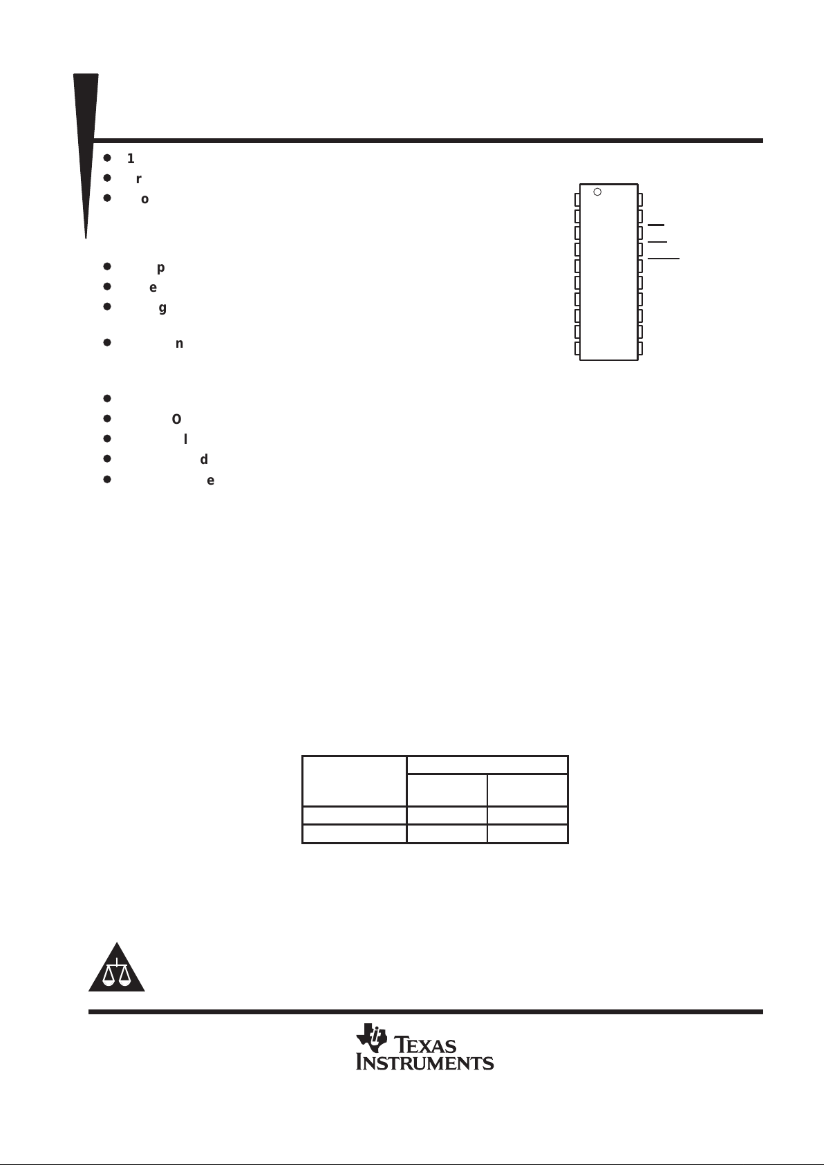
1
2
3
4
5
6
7
8
9
10
20
19
18
17
16
15
14
13
12
11
D2
D3
D4
D5
D6
D7
D8
D9
D10
D11
D1
D0
CS
WE
LDAC
REG
AGND
OUT
REF
V
DD
DW OR PW PACKAGE
(TOP VIEW)
Page 2
TLV5639C, TLV5639I
2.7 V TO 5.5 V LOW POWER 12-BIT DIGITAL-TO-ANALOG
CONVERTERS WITH INTERNAL REFERENCE AND POWER DOWN
SLAS189 – MARCH 1999
2
POST OFFICE BOX 655303 • DALLAS, TEXAS 75265
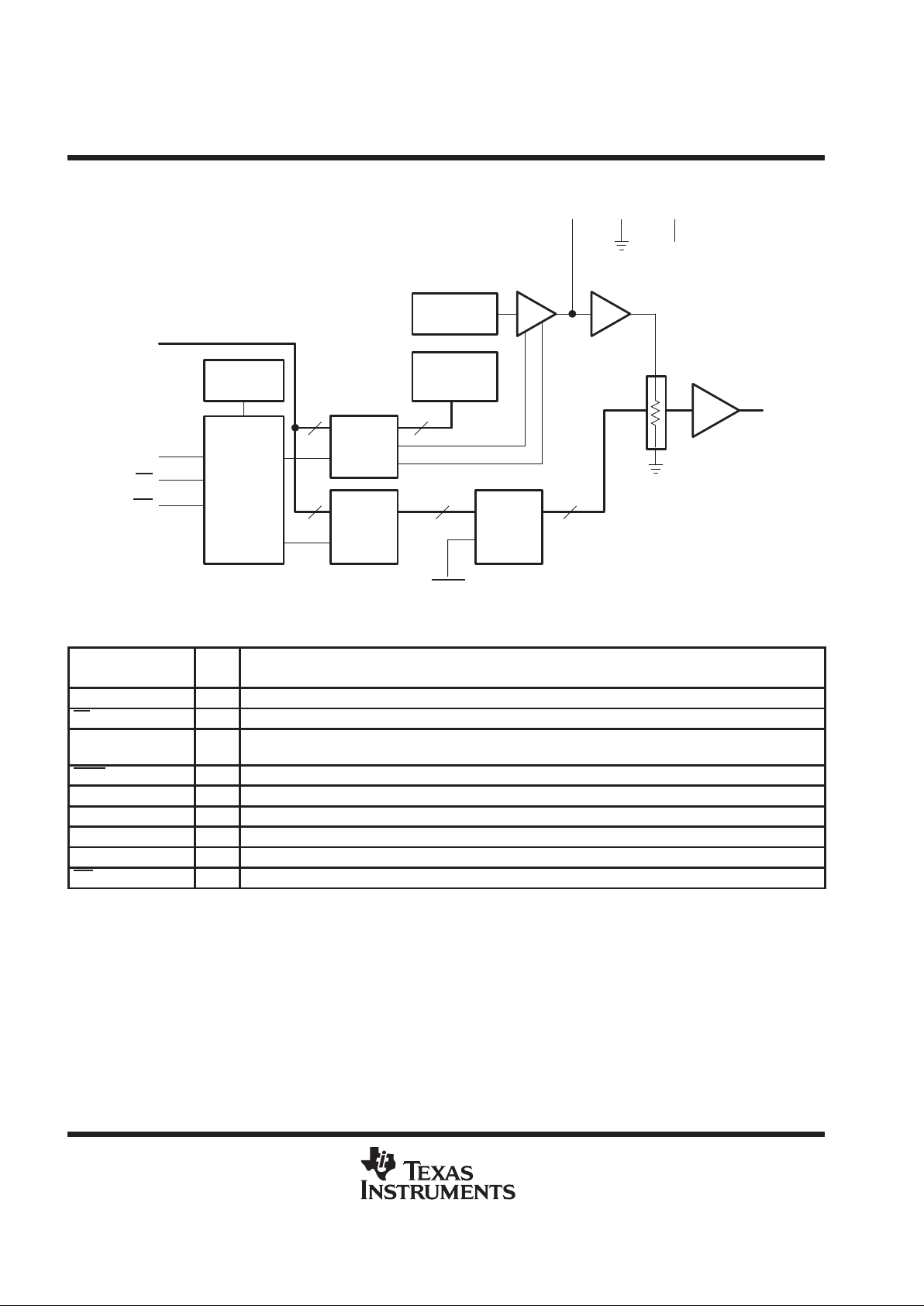
functional block diagram
Interface
Control
12-Bit
DAC
Holding
Latch
D(0–11)
CS
REG
WE
OUT
Power-On
Reset
x2
12
4-Bit
Control
Latch
4
Powerdown
and Speed
Control
2
Voltage
Bandgap
PGA With
Output Enable
12-Bit
DAC
Register
12 12
REF AGND V
DD
LDAC
Terminal Functions
TERMINAL
NAME NO.
I/O/P
DESCRIPTION
AGND 14 P Ground
CS 18 I Chip select. Digital input active low, used to enable/disable inputs
D0 – D11 1 – 10,
19, 20
I Data input
LDAC 16 I Load DAC. Digital input active low, used to load DAC output
OUT 13 O DAC analog voltage output
REG 15 I Register select. Digital input, used to access control register
REF 12 I/O Analog reference voltage input/output
V
DD
11 P Positive power supply
WE 17 I Write enable. Digital input active low, used to latch data
Page 3
TLV5639C, TLV5639I
2.7 V TO 5.5 V LOW POWER 12-BIT DIGITAL-TO-ANALOG
CONVERTERS WITH INTERNAL REFERENCE AND POWER DOWN
SLAS189 – MARCH 1999
3
POST OFFICE BOX 655303 • DALLAS, TEXAS 75265
absolute maximum ratings over operating free-air temperature range (unless otherwise noted)
†
Supply voltage (V
DD
to AGND) 7 V. . . . . . . . . . . . . . . . . . . . . . . . . . . . . . . . . . . . . . . . . . . . . . . . . . . . . . . . . . . . . . .
Reference input voltage range – 0.3 V to V
DD
+ 0.3 V. . . . . . . . . . . . . . . . . . . . . . . . . . . . . . . . . . . . . . . . . . . . . . .
Digital input voltage range – 0.3 V to V
DD
+ 0.3 V. . . . . . . . . . . . . . . . . . . . . . . . . . . . . . . . . . . . . . . . . . . . . . . . . .
Operating free-air temperature range, T
A
: TLV5639C 0°C to 70°C. . . . . . . . . . . . . . . . . . . . . . . . . . . . . . . . . . . .
TLV5639I –40°C to 85°C. . . . . . . . . . . . . . . . . . . . . . . . . . . . . . . . . . .
Storage temperature range, T
stg
–65°C to 150° C. . . . . . . . . . . . . . . . . . . . . . . . . . . . . . . . . . . . . . . . . . . . . . . . . . .
Lead temperature 1,6 mm (1/16 inch) from case for 10 seconds 260°C. . . . . . . . . . . . . . . . . . . . . . . . . . . . . . .
†
Stresses beyond those listed under “absolute maximum ratings” may cause permanent damage to the device. These are stress ratings only, and
functional operation of the device at these or any other conditions beyond those indicated under “recommended operating conditions” is not
implied. Exposure to absolute-maximum-rated conditions for extended periods may affect device reliability.
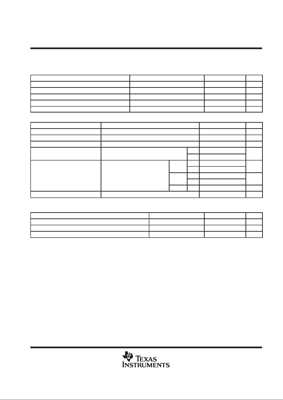
recommended operating conditions
MIN NOM MAX UNIT
pp
VDD = 5 V 4.5 5 5.5 V
Suppl
y v
oltage, V
DD
VDD = 3 V 2.7 3 3.3 V
Power on threshold voltage, POR 0.55 2 V
High-level digital input voltage, V
IH
VDD = 2.7 V to 5.5 V 2 V
Low-level digital input voltage, V
IL
VDD = 2.7 V to 5.5 V 0.8 V
Reference voltage, V
ref
to REF terminal VDD = 5 V (see Note 1) AGND 2.048 VDD–1.5 V
Reference voltage, V
ref
to REF terminal VDD = 3 V (see Note 1) AGND 1.024 VDD–1.5 V
Load resistance, R
L
2 kΩ
Load capacitance, C
L
100 pF
p
p
TLV5639C 0 70
°
Operating free-air temperature, T
A
TLV5639I –40 85
°C
NOTE 1: Due to the x2 output buffer , a reference input voltage ≥ V
DD/2
causes clipping of the transfer function. The output buffer of the internal
reference must be disabled, if an external reference is used.
Page 4
TLV5639C, TLV5639I
2.7 V TO 5.5 V LOW POWER 12-BIT DIGITAL-TO-ANALOG
CONVERTERS WITH INTERNAL REFERENCE AND POWER DOWN
SLAS189 – MARCH 1999
4
POST OFFICE BOX 655303 • DALLAS, TEXAS 75265
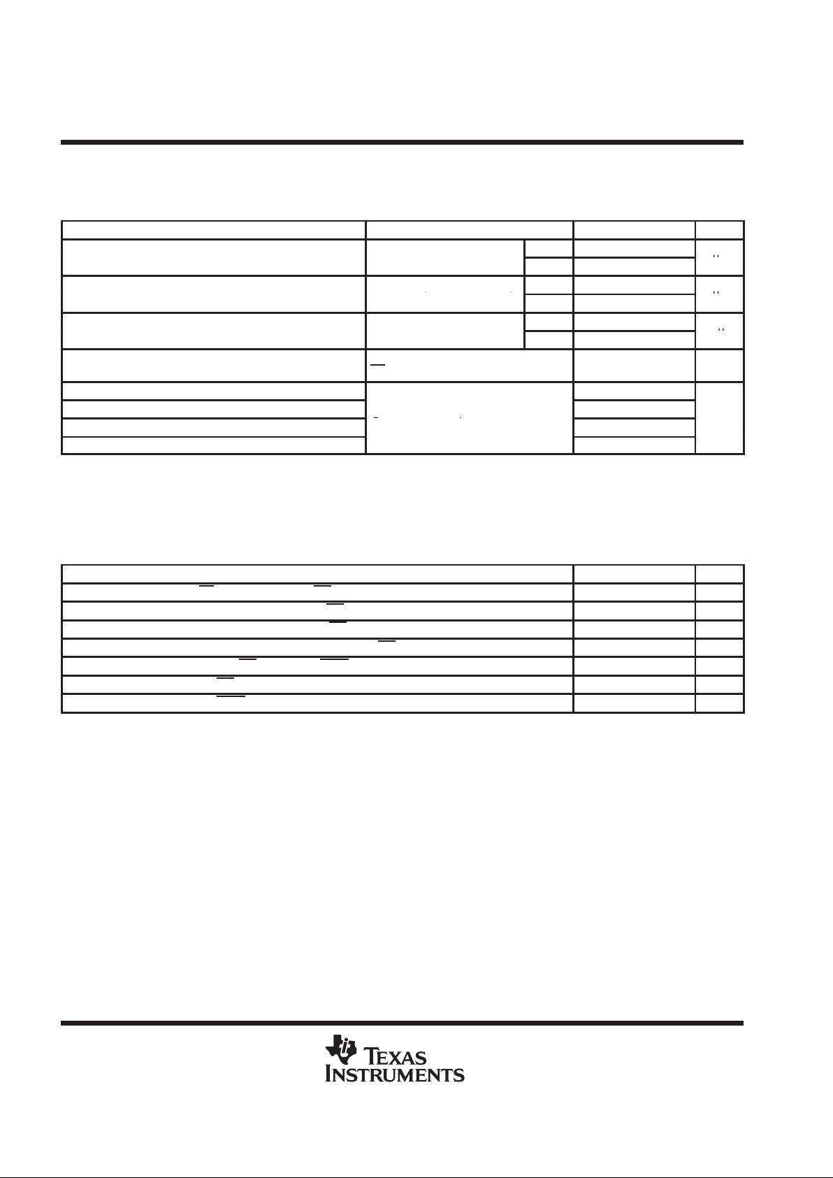
electrical characteristics over recommended operating free-air temperature range, V
ref
= 2.048 V,
V
ref
= 1.024 V (unless otherwise noted)
power supply
PARAMETER TEST CONDITIONS MIN TYP MAX
UNIT
REF
Fast 2.3 2.8 mA
on
Slow 1.3 1.6 mA
V
DD
= 5
V
REF
Fast 1.9 2.4 mA
pp
No load,
p
off
Slow 0.9 1.2 mA
IDDPower supply current
All inputs
=
AGND or V
DD
,
DAC latch = 0x800
REF
Fast 2.1 2.6 mA
on
Slow 1.2 1.5 mA
V
DD
=
3 V
REF
Fast 1.8 2.3 mA
off
Slow 0.9 1.1 mA
Power down supply current 0.01 1 µA
pp
Zero scale, See Note 2, External reference –60
PSRR
Power supply rejection ratio
Full scale, See Note 3, External reference –60
dB
NOTES: 2. Power supply rejection ratio at zero scale is measured by varying VDD and is given by:
PSRR = 20 log [(EZS(VDDmax) – EZS(VDDmin))/VDDmax]
3. Power supply rejection ratio at full scale is measured by varying VDD and is given by:
PSRR = 20 log [(EG(VDDmax) – EG(VDDmin))/VDDmax]
static DAC specifications
PARAMETER TEST CONDITIONS MIN TYP MAX UNIT
Resolution 12 bits
INL Integral nonlinearity , end point adjusted RL = 10 kΩ, CL = 100 pF, See Note 4 ±1.2 ±3 LSB
DNL Differential nonlinearity RL = 10 kΩ, CL = 100 pF, See Note 5 ±0.3 ±0.5 LSB
E
ZS
Zero-scale error (offset error at zero scale) See Note 6 ±12 LSB
EZS TC Zero-scale-error temperature coefficient See Note 7 20 ppm/°C
E
G
Gain error See Note 8 ±0.3
% full
scale V
EG TCGain error temperature coefficient See Note 9 20 ppm/°C
NOTES: 4. The relative accuracy or integral nonlinearity (INL) sometimes referred to as linearity error, is the maximum deviation of the output
from the line between zero and full scale excluding the effects of zero code and full-scale errors (see text).
5. The differential nonlinearity (DNL) sometimes referred to as differential error, is the dif ference between the measured and ideal 1
LSB amplitude change of any two adjacent codes. Monotonic means the output voltage changes in the same direction (or remains
constant) as a change in the digital input code.
6. Zero-scale error is the deviation from zero voltage output when the digital input code is zero (see text).
7. Zero-scale-error temperature coefficient is given by: EZSTC = [EZS(T
max
) – EZS(T
min
)]/2V
ref
× 106/(T
max
– T
min
).
8. Gain error is the deviation from the ideal output (2V
ref
– 1 LSB) with an output load of 10 k excluding the effects of the zero-error.
9. Gain temperature coefficient is given by: EGTC = [EG(T
max
) – EG (T
min
)]/2V
ref
× 106/(T
max
– T
min
).
output specifications
PARAMETER TEST CONDITIONS MIN TYP MAX UNIT
V
O
Output voltage RL = 10 kΩ VDD–0.4 V
Output load regulation accuracy VO = 4.096 V , 2.048 V RL = 2 kΩ ±0.29
% full
scale V
Page 5
TLV5639C, TLV5639I
2.7 V TO 5.5 V LOW POWER 12-BIT DIGITAL-TO-ANALOG
CONVERTERS WITH INTERNAL REFERENCE AND POWER DOWN
SLAS189 – MARCH 1999
5
POST OFFICE BOX 655303 • DALLAS, TEXAS 75265
electrical characteristics over recommended operating free-air temperature range, V
ref
= 2.048 V,
V
ref
= 1.024 V (unless otherwise noted) (Continued)
reference pin configured as output (REF)
PARAMETER TEST CONDITIONS MIN TYP MAX UNIT
V
ref(OUTL)
Low reference voltage 1.003 1.024 1.045 V
V
ref(OUTH)
High reference voltage VDD > 4.75 V 2.027 2.048 2.069 V
I
ref(source)
Output source current 1 mA
I
ref(sink)
Output sink current –1 mA
PSRR Power supply rejection ratio –48 dB
reference pin configured as input (REF)
PARAMETER TEST CONDITIONS MIN TYP MAX UNIT
VIInput voltage 0 V
DD–1.5
V
RIInput resistance 10 MΩ
CIInput capacitance 5 pF
p
Fast 900
Reference input bandwidth
REF
= 0.2
V
pp
+ 1.
024 V dc
Slow 500
kH
z
Fast –87
10 kH
z
Slow –77
dB
Harmonic distortion, reference
p
REF = 1 Vpp + 2.048 V dc, VDD = 5 V
Fast –74
in ut
50 kH
z
Slow –61
dB
100 kHz Fast –66 dB
Reference feedthrough REF = 1 Vpp at 1 kHz + 1.024 V dc (see Note 10) –80 dB
NOTE 10: Reference feedthrough is measured at the DAC output with an input code = 0x000.
digital inputs
PARAMETER TEST CONDITIONS MIN TYP MAX UNIT
I
IH
High-level digital input current VI = V
DD
1 µA
I
IL
Low-level digital input current VI = 0 V –1 µA
C
i
Input capacitance 8 pF
Page 6
TLV5639C, TLV5639I
2.7 V TO 5.5 V LOW POWER 12-BIT DIGITAL-TO-ANALOG
CONVERTERS WITH INTERNAL REFERENCE AND POWER DOWN
SLAS189 – MARCH 1999
6
POST OFFICE BOX 655303 • DALLAS, TEXAS 75265
operating characteristics over recommended operating free-air temperature range, V
ref
= 2.048 V ,
and V
ref
= 1.024 V, (unless otherwise noted)
analog output dynamic performance
PARAMETER TEST CONDITIONS MIN TYP MAX UNIT
p
R
= 10 kΩ,C
= 100 pF,
Fast 1 3
t
s(FS)
Output settling time, full scale
L
,
L
,
See Note 11
Slow 3.5 7
µ
s
p
R
= 10 kΩ,C
= 100 pF,
Fast 0.5 1.5
t
s(CC)
Output settling time, code to code
L
,
L
,
See Note 12
Slow 1 2
µ
s
R
= 10 kΩ,C
= 100 pF,
Fast 6 10
SR
Slew rate
L
,
L
,
See Note 13
Slow 1.2 1.7
V/µs
Glitch energy
DIN = 0 to 1, f
CLK
= 100 kHz,
CS
= V
DD
5 nV–S
SNR Signal-to-noise ratio 73 78
SINAD Signal-to-noise + distortion
fs = 480 kSPS, f
out
= 1 kHz,
61 67
THD Total harmonic distortion
f
B
=
20 kH
z,
R
L
=
10 kΩ
,
C
= 100 pF
–69 –62
dB
SFDR Spurious free dynamic range
C
L
=
100 F
63 74
NOTES: 11. Settling time is the time for the output signal to remain within ±0.5 LSB of the final measured value for a digital input code change
of 0x020 to 0xFDF or 0xFDF to 0x020.
12. Settling time is the time for the output signal to remain within ± 0.5 LSB of the final measured value for a digital input code change
of one count.
13. Slew rate determines the time it takes for a change of the DAC output from 10% to 90% full-scale voltage.
digital input timing requirements
MIN NOM MAX UNIT
t
su(CS–WE)
Setup time, CS low before negative WE edge 15 ns
t
su(D)
Setup time, data ready before positive WE edge 10 ns
t
su(R)
Setup time, REG ready before positive WE edge 20 ns
t
h(DR)
Hold time, data and REG held valid after positive WE edge 5 ns
t
su(WE-LD)
Setup time, positive WE edge before LDAC low 5 ns
t
wH(WE)
Pulse duration, WE high 20 ns
t
w(LD)
Pulse duration, LDAC low 23 ns
Page 7

TLV5639C, TLV5639I
2.7 V TO 5.5 V LOW POWER 12-BIT DIGITAL-TO-ANALOG
CONVERTERS WITH INTERNAL REFERENCE AND POWER DOWN
SLAS189 – MARCH 1999
7
POST OFFICE BOX 655303 • DALLAS, TEXAS 75265
PARAMETER MEASUREMENT INFORMATION
X Data X
X Reg X
t
su(D)
t
su(R)
t
h(DR)
t
wH(WE)
t
su(WE-LD)
t
w(LD)
t
su(CS-WE)
D(0–7)
REG
CS
WE
LDAC
Figure 1. Timing Diagram
Page 8

TLV5639C, TLV5639I
2.7 V TO 5.5 V LOW POWER 12-BIT DIGITAL-TO-ANALOG
CONVERTERS WITH INTERNAL REFERENCE AND POWER DOWN
SLAS189 – MARCH 1999
8
POST OFFICE BOX 655303 • DALLAS, TEXAS 75265
TYPICAL CHARACTERISTICS
–0.4
–1
0 512 1024 1536 2048 2560
DNL – Differential Nonlinearity – LSB
0
0.4
Digital Code
DIFFERENTIAL NONLINEARITY ERROR
1
3072 3584 4096
0.8
0.6
0.2
–0.2
–0.6
–0.8
Figure 2
–2
–3
0 512 1024 1536 2048 2560
INL – Intergral Nonlinearity – LSB
0
1
Digital Code
INTEGRAL NONLINEARITY ERROR
3
3072 3584 4096
2
–1
Figure 3
Page 9

TLV5639C, TLV5639I
2.7 V TO 5.5 V LOW POWER 12-BIT DIGITAL-TO-ANALOG
CONVERTERS WITH INTERNAL REFERENCE AND POWER DOWN
SLAS189 – MARCH 1999
9
POST OFFICE BOX 655303 • DALLAS, TEXAS 75265
TYPICAL CHARACTERISTICS
Figure 4
2.0385
2.037
2.036
2.0355
0 0.5 1 1.5 2 2.5 3
– Output Voltage – V
2.039
2.0395
Load Current – mA
MAXIMUM OUTPUT VOLTAGE
vs
LOAD CURRENT
2.04
3.5 4 4.5
2.038
2.0375
2.0365
V
O
Fast Mode, Source
Slow Mode, Source
VDD = 3 V,
V
ref
= Int. 1 V,
Input Code = 0xFFF
Figure 5
4.078
4.077
4.076
4.0755
0 0.5 1 1.5 2 2.5 3
4.079
4.0795
MAXIMUM OUTPUT VOLTAGE
vs
LOAD CURRENT
4.08
3.5 4 4.5
4.0785
4.0775
4.0765
– Output Voltage – V
Load Current – mA
V
O
Fast Mode, Source
Slow Mode, Source
VDD = 5 V,
V
ref
= Int. 2 V,
Input Code = 0xFFF
Figure 6
0.1
0.05
0
0 0.5 1 1.5 2 2.5 3
0.15
0.2
0.25
3.5 4 4.5
MINIMUM OUTPUT VOLTAGE
vs
LOAD CURRENT
– Output Voltage – V
Load Current – mA
V
O
Fast Mode, Sink
Slow Mode, Sink
VDD = 5 V,
V
ref
= Int. 2 V,
Input Code = 0x000
Figure 7
0.1
0.05
0
0 0.5 1 1.5 2 2.5 3
0.15
0.2
0.25
3.5 4 4.5
MINIMUM OUTPUT VOLTAGE
vs
LOAD CURRENT
– Output Voltage – V
Load Current – mA
V
O
Fast Mode, Sink
Slow Mode, Sink
VDD = 3 V,
V
ref
= Int. 1 V,
Input Code = 0x000
Page 10

TLV5639C, TLV5639I
2.7 V TO 5.5 V LOW POWER 12-BIT DIGITAL-TO-ANALOG
CONVERTERS WITH INTERNAL REFERENCE AND POWER DOWN
SLAS189 – MARCH 1999
10
POST OFFICE BOX 655303 • DALLAS, TEXAS 75265
TYPICAL CHARACTERISTICS
Figure 8
–40
–60
–80
–100
100 1000
THD – Total Harmonic Distortion – dB
–30
–10
f – Frequency – Hz
TOTAL HARMONIC DISTORTION
vs
FREQUENCY
0
10000 100000
–20
–50
–70
–90
Slow Mode
Fast Mode
VDD = 5 V,
REF = 1 V dc + 1 V pp Sinewave,
Output Full Scale
Figure 9
–40
–60
–80
–100
100 1000
THD+N – Total Harmonic Distortion and Noise – dB
–30
–10
f – Frequency – Hz
TOTAL HARMONIC DISTORTION AND NOISE
vs
FREQUENCY
0
10000 100000
–20
–50
–70
–90
Slow Mode
Fast Mode
VDD = 5 V,
REF = 1 V dc + 1 V pp Sinewave,
Output Full Scale
0.5
0.4
0.2
0
0102030405060
– Supply Current – mA
0.7
0.9
POWER DOWN SUPPLY CURRENT
vs
TIME
1
70 80 90
0.8
0.6
0.3
0.1
t – Time – µs
I
DD
Figure 10
Page 11

TLV5639C, TLV5639I
2.7 V TO 5.5 V LOW POWER 12-BIT DIGITAL-TO-ANALOG
CONVERTERS WITH INTERNAL REFERENCE AND POWER DOWN
SLAS189 – MARCH 1999
11
POST OFFICE BOX 655303 • DALLAS, TEXAS 75265
APPLICATION INFORMATION
general function
The TLV5639 is a 12-bit, single supply DAC, based on a resistor string architecture. It consists of a parallel
interface, a speed and power down control logic, a programmable internal reference, a resistor string, and a
rail-to-rail output buffer. The output voltage (full scale determined by reference) is given by:
2REF
CODE
0x1000
[V]
Where REF is the reference voltage and CODE is the digital input value in the range 0x000 to 0xFFF. A power
on reset initially puts the internal latches to a defined state (all bits zero).
parallel interface
The device latches data on the positive edge of WE. It must be enabled with CS low. Whether the data is written
to the DAC holding latch or the control register depends on REG. REG = 0 selects the DAC holding latch,
REG = 1 selects the control register. LDAC
low updates the DAC with the value in the holding latch. LDAC is
an asynchronous input and can be held low, if a separate update is not necessary . However , to control the DAC
using the load feature, there should be approximately a 5 ns delay after the positive WE
edge before driving
LDAC
low.
Address
Decoder
A(0–15)
IS
WE
D(0–15)
CS
LDAC
WE
D(0–11)
TMS320C2XX, 5X
TLV5639
Address
Decoder
A(0–15)
TCLK0
R/W
D(0–15)
CS
LDAC
WE
D(0–11)
TMS320C3X
TLV5639
IOSTROBE
REG
> = 1
REG
Figure 11
data format
The TL V5639 writes data either to the DAC holding latch or to the control register, depending on the level of the
REG input.
Data destination:
REG = 0 → DAC holding latch
REG = 1 → control register
Page 12

TLV5639C, TLV5639I
2.7 V TO 5.5 V LOW POWER 12-BIT DIGITAL-TO-ANALOG
CONVERTERS WITH INTERNAL REFERENCE AND POWER DOWN
SLAS189 – MARCH 1999
12
POST OFFICE BOX 655303 • DALLAS, TEXAS 75265
APPLICATION INFORMATION
The following table lists the meaning of the bits within the control register:
D11 D10 D9 D8 D7 D6 D5 D4 D3 D2 D1 D0
X X X X X X X REF1 REF0 X PWR SPD
X
†
X
†
X
†
X
†
X
†
X
†
X
†
0
†
0
†
X
†
0
†
0
†
†
Default values
X: don’t care
SPD: Speed control bit 1 → fast mode 0 → slow mode
PWR: Power control bit 1 → power down 0 → normal operation
REF1 and REF0 determine the reference source and the reference voltage.
REFERENCE BITS
REF1
REF0 REFERENCE
0 0 External
0 1 2.048 V
1 0 1.024 V
1 1 External
If an external reference voltage is applied to the REF pin, external reference must be selected.
linearity, offset, and gain error using single end supplies
When an amplifier is operated from a single supply , the voltage offset can still be either positive or negative. With
a positive offset, the output voltage changes on the first code change. With a negative offset the output voltage
may not change with the first code depending on the magnitude of the offset voltage.
The output amplifier attempts to drive the output to a negative voltage. However, because the most negative
supply rail is ground, the output cannot drive below ground and clamps the output at 0 V.
The output voltage remains at zero until the input code value produces a sufficient positive output voltage to
overcome the negative offset voltage, resulting in the transfer function shown in Figure 12.
DAC Code
Output
Voltage
0 V
Negative
Offset
Figure 12. Effect of Negative Offset (Single Supply)
This offset error , not the linearity error, produces this breakpoint. The transfer function would have followed the
dotted line if the output buffer could drive below the ground rail.
For a DAC, linearity is measured between zero input code (all inputs 0) and full scale code (all inputs 1) after
offset and full scale are adjusted out or accounted for in some way . However , single supply operation does not
allow for adjustment when the offset is negative due to the breakpoint in the transfer function. So the linearity
is measured between full scale code and the lowest code that produces a positive output voltage.
Page 13

TLV5639C, TLV5639I
2.7 V TO 5.5 V LOW POWER 12-BIT DIGITAL-TO-ANALOG
CONVERTERS WITH INTERNAL REFERENCE AND POWER DOWN
SLAS189 – MARCH 1999
13
POST OFFICE BOX 655303 • DALLAS, TEXAS 75265
APPLICATION INFORMATION
TLV5639 interfaced to TMS320C203 DSP
hardware interface
Figure 13 shows an example of the connection between the TLV5639 and the TMS320C203 DSP. The only
other device that is needed in addition to the DSP and the DAC is the 74AC138 address decoding circuit . Using
this configuration, the DAC data is at address 0x0084 and the DAC control word is at address 0x0085 within
the I/O memory space of the TMS320C203.
LDAC
is tied low so that the output voltage is updated on the rising WE edge.
A2
A3
A4
A6
IS
D(0–11)
5 V
A
B
C
G1
G2A
G2B
CS
D(0–11)
Y1
WE
REF
To Other Devices Requiring
Voltage Reference
OUT
LDAC
WE
R
LOAD
TMS320C203 74AC138
TLV5639
12
REG
A0
Figure 13. TLV5639 to TMS320C203 DSP Interface Connection
software
Writing data or control information to the TLV5639 is done using a single command. For example, the line of
code which reads:
out 62h, dac_ctrl
writes the contents of address 0x0062 to the I/O address equated to dac_ctrl (0x0085, the address where
the DAC control register has been mapped).
The following code shows how to set the DAC up to use the internal reference and operate in FAST mode by
a write to the control register. Timer interrupts are then enabled and repeatedly generated every 205 µs to
provide a timebase for synchonizing the waveform generation. In this example, the waveform is generated by
simply incrementing a counter and outputting the counter value to the DAC data word once every timer interrupt.
This results in a saw waveform.
Page 14

TLV5639C, TLV5639I
2.7 V TO 5.5 V LOW POWER 12-BIT DIGITAL-TO-ANALOG
CONVERTERS WITH INTERNAL REFERENCE AND POWER DOWN
SLAS189 – MARCH 1999
14
POST OFFICE BOX 655303 • DALLAS, TEXAS 75265
APPLICATION INFORMATION
; File: RAMP.ASM
; Function: ramp generation with TLV5639
; Processors: TMS320C203
; 1999 Texas Instruments
;–––––––––– I/O and memory mapped regs –––––––––––––––
.include “regs.asm”
dac_data .equ 0084h
dac_ctrl .equ 0085h
;––––––––––––– vectors –––––––––––––––––––––––––––––––
.ps 0h
b start
b INT1
b INT23
b TIM_ISR
––––––––––Main Program––––––––––
.ps 1000h
.entry
start:
ldp #0 ; set data page to 0
; disable interrupts
setc INTM
; disable maskable interrupts
splk #0ffffh, IFR
splk #0004h, IMR
; set up the timer
splk #0000h, 60h
splk #0042h, 61h
out 61h, PRD
out 60h, TIM
splk #0c2fh, 62h
out 62h, TCR
splk #0011h, 62h ; set up the DAC
; SPD=1 (FAST mode) and ; REF1=1 (2.048 V internal ref enable)
out 62h, dac_ctrl
clrc INTM ; enable interrupts
; loop forever!
next idle
b next
–––––––––– Interrupt Service Routines––––––––––
INT1: ret ; do nothing and return
INT23: ret ; do nothing and return
TIM_ISR:
; timer interrupt handler
add #1h ; increment accumulator
sacl 60h
out 60h, dac_data ; write to DAC
clrc intm ; re-enable interrupts
ret ; return from interrupt
.END
Page 15

TLV5639C, TLV5639I
2.7 V TO 5.5 V LOW POWER 12-BIT DIGITAL-TO-ANALOG
CONVERTERS WITH INTERNAL REFERENCE AND POWER DOWN
SLAS189 – MARCH 1999
15
POST OFFICE BOX 655303 • DALLAS, TEXAS 75265
MECHANICAL DATA
DW (R-PDSO-G**) PLASTIC SMALL-OUTLINE PACKAGE
16 PIN SHOWN
4040000/D 02/98
Seating Plane
0.400 (10,15)
0.419 (10,65)
0.104 (2,65) MAX
1
0.012 (0,30)
0.004 (0,10)
A
8
16
0.020 (0,51)
0.014 (0,35)
0.293 (7,45)
0.299 (7,59)
9
0.010 (0,25)
0.050 (1,27)
0.016 (0,40)
(15,24)
(15,49)
PINS **
0.010 (0,25) NOM
A MAX
DIM
A MIN
Gage Plane
20
0.500
(12,70)
(12,95)
0.510
(10,16)
(10,41)
0.400
0.410
16
0.600
24
0.610
0.004 (0,10)
M
0.010 (0,25)
0.050 (1,27)
0°–8°
NOTES: A. All linear dimensions are in inches (millimeters).
B. This drawing is subject to change without notice.
C. Body dimensions do not include mold flash or protrusion not to exceed 0.006 (0,15).
D. Falls within JEDEC MS-013
Page 16

TLV5639C, TLV5639I
2.7 V TO 5.5 V LOW POWER 12-BIT DIGITAL-TO-ANALOG
CONVERTERS WITH INTERNAL REFERENCE AND POWER DOWN
SLAS189 – MARCH 1999
16
POST OFFICE BOX 655303 • DALLAS, TEXAS 75265
MECHANICAL DATA
PW (R-PDSO-G**) PLASTIC SMALL-OUTLINE PACKAGE
4040064/E 08/96
14 PIN SHOWN
Seating Plane
0,05 MIN
1,20 MAX
1
A
7
14
0,19
4,50
4,30
8
6,20
6,60
0,30
0,75
0,50
0,25
Gage Plane
0,15 NOM
0,65
M
0,10
0°–8°
0,10
PINS **
A MIN
A MAX
DIM
2,90
3,10
8
4,90
5,10
14
6,60
6,404,90
5,10
16
7,70
20
7,90
24
9,60
9,80
28
NOTES: A. All linear dimensions are in millimeters.
B. This drawing is subject to change without notice.
C. Body dimensions do not include mold flash or protrusion not to exceed 0,15.
D. Falls within JEDEC MO-153
Page 17

IMPORTANT NOTICE
T exas Instruments and its subsidiaries (TI) reserve the right to make changes to their products or to discontinue
any product or service without notice, and advise customers to obtain the latest version of relevant information
to verify, before placing orders, that information being relied on is current and complete. All products are sold
subject to the terms and conditions of sale supplied at the time of order acknowledgement, including those
pertaining to warranty, patent infringement, and limitation of liability.
TI warrants performance of its semiconductor products to the specifications applicable at the time of sale in
accordance with TI’s standard warranty. Testing and other quality control techniques are utilized to the extent
TI deems necessary to support this warranty. Specific testing of all parameters of each device is not necessarily
performed, except those mandated by government requirements.
CERT AIN APPLICATIONS USING SEMICONDUCTOR PRODUCTS MAY INVOLVE POTENTIAL RISKS OF
DEATH, PERSONAL INJURY, OR SEVERE PROPERTY OR ENVIRONMENTAL DAMAGE (“CRITICAL
APPLICATIONS”). TI SEMICONDUCTOR PRODUCTS ARE NOT DESIGNED, AUTHORIZED, OR
WARRANTED TO BE SUITABLE FOR USE IN LIFE-SUPPORT DEVICES OR SYSTEMS OR OTHER
CRITICAL APPLICATIONS. INCLUSION OF TI PRODUCTS IN SUCH APPLICA TIONS IS UNDERST OOD TO
BE FULLY AT THE CUSTOMER’S RISK.
In order to minimize risks associated with the customer’s applications, adequate design and operating
safeguards must be provided by the customer to minimize inherent or procedural hazards.
TI assumes no liability for applications assistance or customer product design. TI does not warrant or represent
that any license, either express or implied, is granted under any patent right, copyright, mask work right, or other
intellectual property right of TI covering or relating to any combination, machine, or process in which such
semiconductor products or services might be or are used. TI’s publication of information regarding any third
party’s products or services does not constitute TI’s approval, warranty or endorsement thereof.
Copyright 1999, Texas Instruments Incorporated
 Loading...