

Page 1

TLV320AIC27
STEREO AUDIO CODEC
SLAS253 – MARCH 2000
D
3.3-V or 5-V Operation
D
18-Bit Stereo Codec
D
S/N Ratio >95 dB
D
Multiple Stereo Input Mixer
D
Mono and Stereo Volume Control
D
48-Pin TQFP Package
D
Power Management Features
D
Low-Power Implementation
description
The TL V320AIC27 comprises a stereo 18-bit codec (that is, 2 ADCs and 4 DACs), plus a comprehensive analog
mixer with four sets of stereo inputs, plus one phone input, two microphone inputs, and one PC-beep input.
Additionally , on-chip reference circuits generate the necessary bias voltages for the device, and a bidirectional
serial interface allows transfer of control data, DAC, and ADC words to and from the AC’97 controller. The
TLV320AIC27 is fully compliant with Revision 2.1 of the AC’97 specification.
The TLV320AIC27 has the ADC and DAC functions implemented using oversampled, or sigma-delta,
converters and uses on-chip digital filters to convert these one-bit signals to and from the 48 ksps, 16/18-bit PCM
words that the AC’97 controller requires. The digital and analog sections of the device are powered separately
to optimize performance, and 3.3-V digital and 5-V analog supplies may be used on the same device to further
optimize performance. Digital IOs are 5-V tolerant when the analog supplies are 5 V. Therefore, the
TLV320AIC27 may be connected to a controller running on 5-V supplies, but use 3.3 V for the digital section
of the TLV320AIC27. The TLV320AIC27 is also capable of operating with a 3.3-V supply only (digital and
analog).
D
Four DAC Channels, Stereo ADC
D
Balanced Mixer Architecture
D
Variable Rate Audio and Modem Support
D
Analog 3D Stereo Enhancement
D
Line Level Outputs
D
Master/Slave ID Selection
D
AC97 Rev. 2.1 Compliant
D
Complete TI-DSP-CODEC Solution
When using the TL V320AIC27 codec, the AC’97 controller may be selected from Texas Instruments family of
DSPs. The combination of the computing power of the TI DSP and the high audio performance of the
TLV320AIC27 constitutes a complete solution for various applications. The ability to power down sections of
the device selectively, and the option to alternate the master clock, and hence sample rates, makes such
applications as telecommunications, audio, teleconferencing, and USB, possible.
Additional features added to the Intel AC’97 specification, such as the EAPD (external amplifier power down)
bit and internal connection of PC beep to the outputs when the device is reset are supported, as well as optional
features such as variable sample rate support.
There are four modes of operation.
D
Basic (2-channel)
D
6-channel I2S
D
Quad
D
Modem
ESD Sensitive Device. This device is manufactured on a CMOS process. It it therefore generically susceptible to damage from
excessive static voltages. Proper ESD precautions must be taken during handling and storage of this device. As per JEDEC
specifications A112-A and A113-B, this product requires specific storage conditions prior to surface mount assembly. It has been
classified as having a Moisture Sensitivity Level of 2 and as such will be supplied in vacuum-sealed moisture barrier bags.
Please be aware that an important notice concerning availability, standard warranty, and use in critical applications of
Texas Instruments semiconductor products and disclaimers thereto appears at the end of this data sheet.
Intel is a trademark of Intel Corporation.
PRODUCTION DATA information is current as of publication date.
Products conform to specifications per the terms of Texas Instruments
standard warranty. Production processing does not necessarily include
testing of all parameters.
POST OFFICE BOX 655303 • DALLAS, TEXAS 75265
Copyright 2000, Texas Instruments Incorporated
1
Page 2
TLV320AIC27
T
STEREO AUDIO CODEC
SLAS253 – MARCH 2000
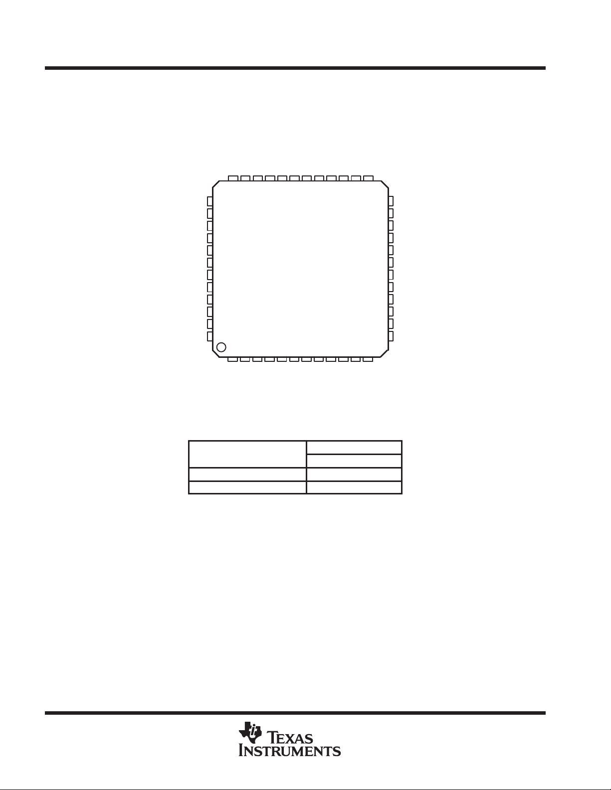
terminal assignments
LINEOUTR
LINEOUTL
CX3D2
CX3D1
PFB PACKAGE
(TOP VIEW)
CAP1
MODE0
AFILT1
CAP2
SS1
VREFOUT
VREF
AV
DD1
AV
MONOOUT
AV
DD2
LNLVLOUTL
MODE1
LNLVLOUTR
AV
SS2
GPIO
GPIO
CID0
CID1
EAPD
GPIO
35 34 33 32 3136 30
37
38
39
40
41
42
43
44
45
46
47
48
23
1
DD1
XTLIN
DV
5678
4
SS1
DV
XTLOUT
SS2
DV
BITCLK
28 27 2629
9
SDATAIN
10 11 12
DD2
SYNC
DV
25
RESETB
SDATAOUT
ORDERING INFORMATION
A
0°C to 70°C TLV320AIC27CPFB
–40°C to 85°C TLV320AIC27IPFB
PACKAGE
48-TQFP PFB
LINEINR
24
LINEINL
23
MIC2
22
21
MIC1
20
CDR
CDGND
19
CDL
18
VIDEOR
17
VIDEOL
16
AUXR
15
AUXL
14
PHONE
13
PCBEEP
2
POST OFFICE BOX 655303 • DALLAS, TEXAS 75265
Page 3
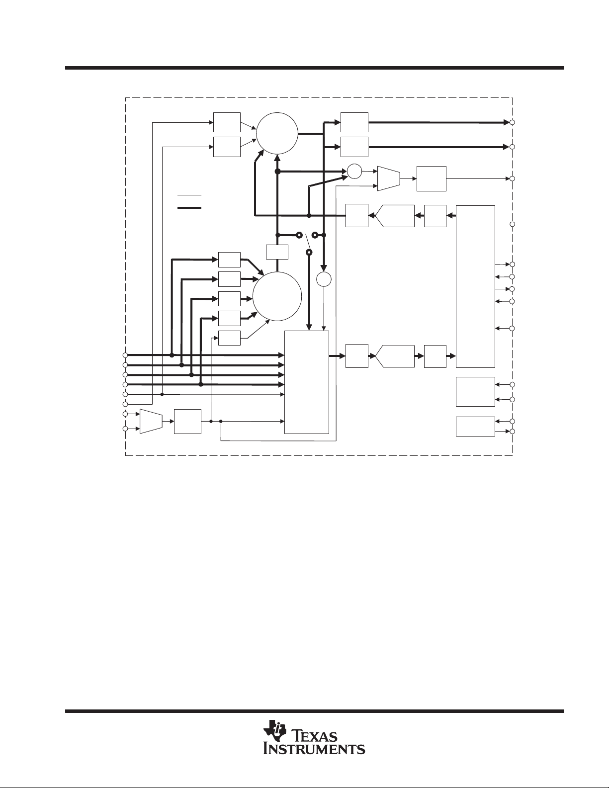
functional block diagram—two-channel mode
TLV320AIC27
STEREO AUDIO CODEC
SLAS253 – MARCH 2000
CD (18,20)
LINEIN (23,24)
VIDEO (16,17)
AUX (14,15)
PHONE (13)
PCBEEP (12)
MIC[1] (21)
MIC[2] (22)
MUX
KEY:
0dB/
20dB
VOL/
MUTE
VOL/
MUTE
MONO
STEREO
VOL/
MUTE
VOL/
MUTE
VOL/
MUTE
VOL/
MUTE
VOL/
MUTE
∑
3D
∑
RECORD
MUX
AND
MUTE
VOL/
MUTE
VOL/
MUTE
∑
MUX
VOL
∑
VOL
STEREO
DAC
STEREO
DAC
VOL/
MUTE
SRC
SERIAL
I/F
SRC
MASTER/
SLAVE
SELECT
OSC
(35,36)
LINEOUT
(39,41)
LNLVLOUT
(37)
MONOOUT
(47) EAPD
(6) BITCLK
(10) SYNC
(8)
SDATAIN
(5)
SDATAOUT
(11)
RESETB
(45)CID[0]
(46)CID[1]
(2) XTLIN
(3) XTLOUT
POST OFFICE BOX 655303 • DALLAS, TEXAS 75265
3
Page 4
TLV320AIC27
STEREO AUDIO CODEC
SLAS253 – MARCH 2000
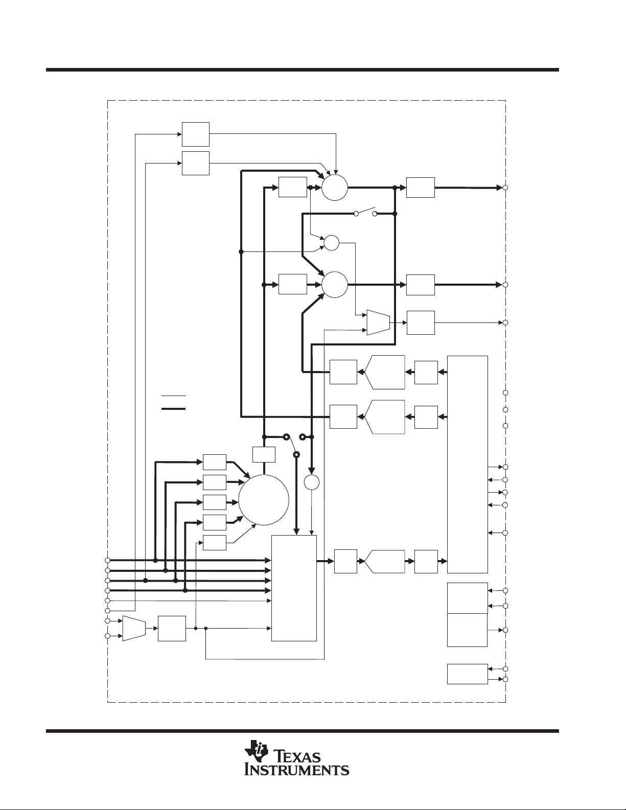
functional block diagram—6-channel I2S, quad, and modem modes
VOL/
MUTE
VOL/
MUTE
VOL/
MUTE
∑
∑
REV . 2.1
SWITCH
VOL/
MUTE
(35,36)
LINEOUT
(FRONT)
CD (18,20)
LINEIN (23,24)
VIDEO (16,17)
AUX (14,15)
PHONE (13)
PCBEEP (12)
MIC[1] (21)
MIC[2] (22)
MUX
KEY:
0dB/
20dB
MONO
STEREO
VOL/
MUTE
VOL/
MUTE
VOL/
MUTE
VOL/
MUTE
VOL/
MUTE
3D
∑
VOL/
MUTE
RECORD
MUX
AND
MUTE
∑
MUX
VOL/
MUTE
VOL/
MUTE
∑
VOL
REAR
STEREO
DAC
FRONT
STEREO
DAC
STEREO
ADC
VOL/
MUTE
VOL/
MUTE
SRC
SRC
SRC
SERIAL
I/F
MASTER/
SLAVE
SELECT
General
Supprt GPIO[1:3]
(39,41)
LINEOUT
(REAR)
(37)
MONOOUT
(40) MODE1
(30) MODE0
(47) EAPD
(6) BITCLK
(10) SYNC
(8)
SDATAIN
(5)
SDATAOUT
(11)
RESETB
(45)CID[0]
(46)CID[1]
(43,44,48)IO
OSC
4
POST OFFICE BOX 655303 • DALLAS, TEXAS 75265
(2) XTLIN
(3) XTLOUT
Page 5

TYPE
DESCRIPTION
STEREO AUDIO CODEC
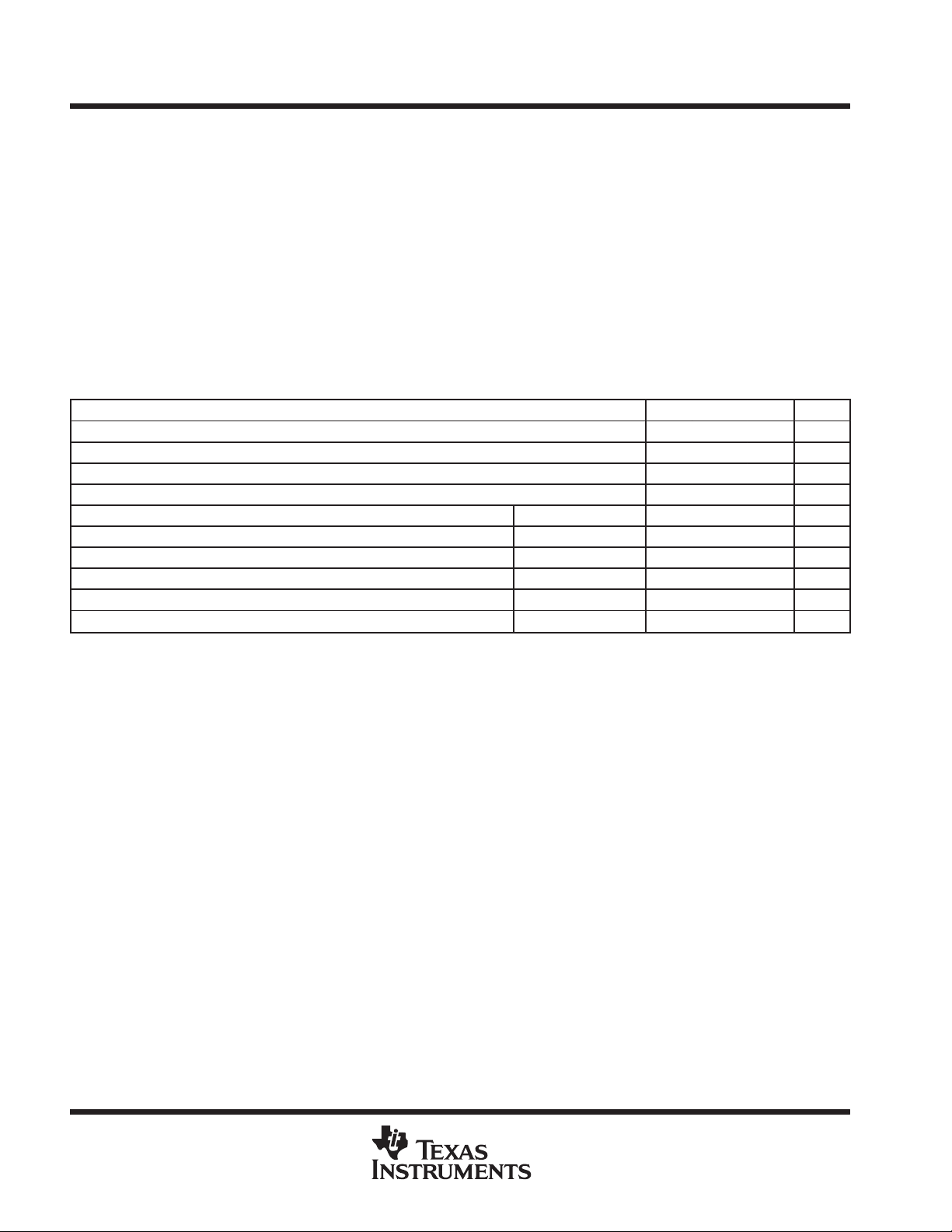
Terminal Functions
TERMINAL
NAME NO.
AFILT1 29 Analog output Buffered CAP2. This terminal has an internal connection.
VIDEOL 16 Analog input Mixer input, typically for VIDEO signal
VIDEOR 17 Analog input Mixer input, typically for VIDEO signal
AUXL 14 Analog input Mixer input, typically for AUX signal
AUXR 15 Analog input Mixer input, typically for AUX signal
AV
DD1
AV
DD2
AV
SS1
AV
SS2
BITCLK 6 Digital output Serial interface clock output to AC’97 controller
CAP1 31 Analog output Buffered CAP2. This terminal has an internal connection.
CAP2 32 Analog input Reference input/output; pulls to midrail if not driven
CDGND 19 Analog input CD input common-mode reference (ground)
CDL 18 Analog input Mixer input, typically for CD signal
CDR 20 Analog input Mixer input, typically for CD signal
CID0 45 Digital input Master/slave ID select (internal pullup)
CID1 46 Digital input Master/slave ID select (internal pullup)
CX3D1 33 Analog output Output pin for 3D difference signal
CX3D2 34 Analog input Input pin for 3D difference signal
DV
DD1
DV
DD2
DV
SS1
DV
SS2
EAPD 47 Digital output External amplifier power down/GPO
GPIO 43, 44, 48 General-purpose I/O
LINEINL 23 Analog input Mixer input, typically for LINE signal
LINEINR 24 Analog input Mixer input, typically for LINE signal
LINEOUTL 35 Analog output Main analog output for left channel
LINEOUTR 36 Analog output Main analog output for right channel
LNLVLOUTL 39 Analog output Left channel line-level output
LNLVLOUTR 41 Analog output Right channel line-level output
MIC1 21 Analog input Mixer input with extra gain, if required
MIC2 22 Analog input Mixer input with extra gain, if required
MONOOUT 37 Analog output Main mono output
MODE0 30 Digital input Mode select pin, internal pulldown
MODE1 40 Digital input Mode select pin, internal pulldown
PCBEEP 12 Analog input Mixer input, typically for PCBEEP signal
PHONE 13 Analog input Mixer input, typically for PHONE signal
RESETB 11 Digital input NOT reset input (active low, resets registers)
SDATAIN 8 Digital output Serial-data output to AC’97 controller
SDATAOUT 5 Digital input Serial-data input
SYNC 10 Digital input Serial-interface sync pulse from AC’97 controller
VREF 27 Analog output Buffered CAP2. This terminal has an internal connection.
VREFOUT 28 Analog output Reference for microphones; buffered CAP2
XTLIN 2 Digital input Clock-crystal connection or clock input (XTAL not used)
XTLOUT 3 Digital output Clock-crystal connection
25 Supply Analog positive supply
38 Supply Analog positive supply
26 Supply Analog ground supply, chip substrate
42 Supply Analog ground supply, chip substrate
1 Supply Digital positive supply
9 Supply Digital positive supply
4 Supply Digital ground supply
7 Supply Digital ground supply
TLV320AIC27
SLAS253 – MARCH 2000
POST OFFICE BOX 655303 • DALLAS, TEXAS 75265
5
Page 6
TLV320AIC27
STEREO AUDIO CODEC
SLAS253 – MARCH 2000
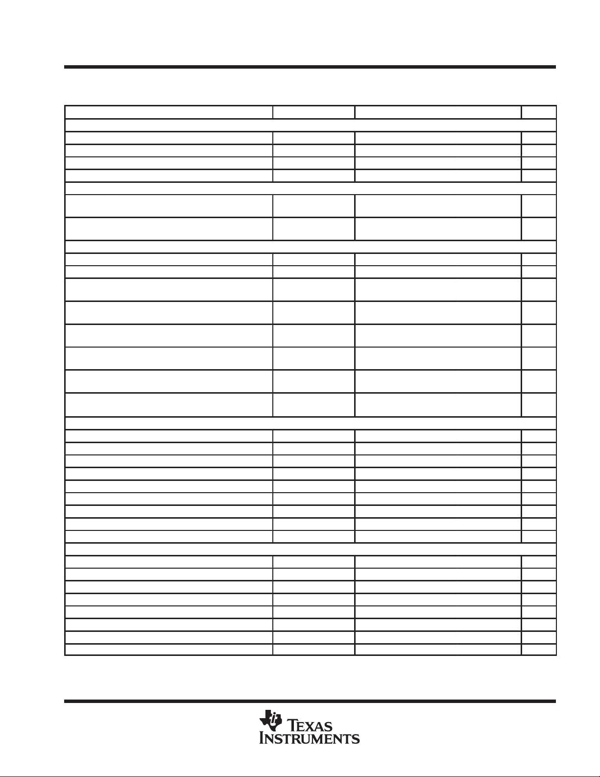
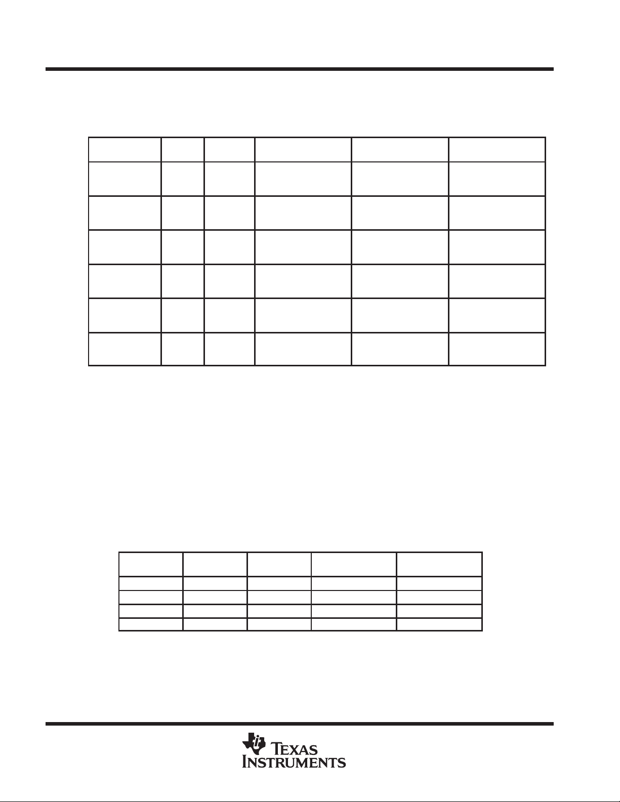
absolute maximum ratings over operating free-air temperature (unless otherwise noted)
†
Digital supply voltage –0.3 V to 7 V. . . . . . . . . . . . . . . . . . . . . . . . . . . . . . . . . . . . . . . . . . . . . . . . . . . . . . . . . . . . . .
Analog supply voltage –0.3 V to 7 V. . . . . . . . . . . . . . . . . . . . . . . . . . . . . . . . . . . . . . . . . . . . . . . . . . . . . . . . . . . . . .
Voltage range digital inputs DV
Voltage range analog inputs AV
SS
DD
–0.3 V to DVDD +0.3 V. . . . . . . . . . . . . . . . . . . . . . . . . . . . . . . . . . . . . . . . . . . .
–0.3 V to AVDD +0.3 V. . . . . . . . . . . . . . . . . . . . . . . . . . . . . . . . . . . . . . . . . . .
Operating temperature range, TA 0°C to 70°C. . . . . . . . . . . . . . . . . . . . . . . . . . . . . . . . . . . . . . . . . . . . . . . . . . . . .
Storage temperature –65°C to 150°C. . . . . . . . . . . . . . . . . . . . . . . . . . . . . . . . . . . . . . . . . . . . . . . . . . . . . . . . . . . . .
Lead temperature (soldering 10 seconds) 260°C. . . . . . . . . . . . . . . . . . . . . . . . . . . . . . . . . . . . . . . . . . . . . . . . . . .
Lead temperature (soldering 2 minutes) 183°C. . . . . . . . . . . . . . . . . . . . . . . . . . . . . . . . . . . . . . . . . . . . . . . . . . . . .
†
Stresses beyond those listed under “absolute maximum ratings” may cause permanent damage to the device. These are stress ratings only, and
functional operation of the device at these or any other conditions beyond those indicated under “recommended operating conditions” is not
implied. Exposure to absolute-maximum-rated conditions for extended periods may affect device reliability.
recommended operating conditions
MIN TYP MAX UNIT
Digital supply range, DV
Analog supply range, AV
Digital ground, DV
Analog ground, AV
Analog supply current DVDD, AVDD = 5 V 35 50 mA
Digital supply current DVDD, AVDD = 5 V 30 50 mA
Standby supply current (all PRs set) DVDD, AVDD = 5 V 150 600 µA
Analog supply current DVDD, AVDD = 3.3 V 22 33 mA
Digital supply current DVDD, AVDD = 3.3 V 20 22 mA
Standby supply current (all PRs set) DVDD, AVDD = 3.3 V 100 150 µA
DD
DD
SS
SS
3.3 to 5 V
3.3 to 5 V
0 V
0 V
6
POST OFFICE BOX 655303 • DALLAS, TEXAS 75265
Page 7
TLV320AIC27
STEREO AUDIO CODEC
SLAS253 – MARCH 2000
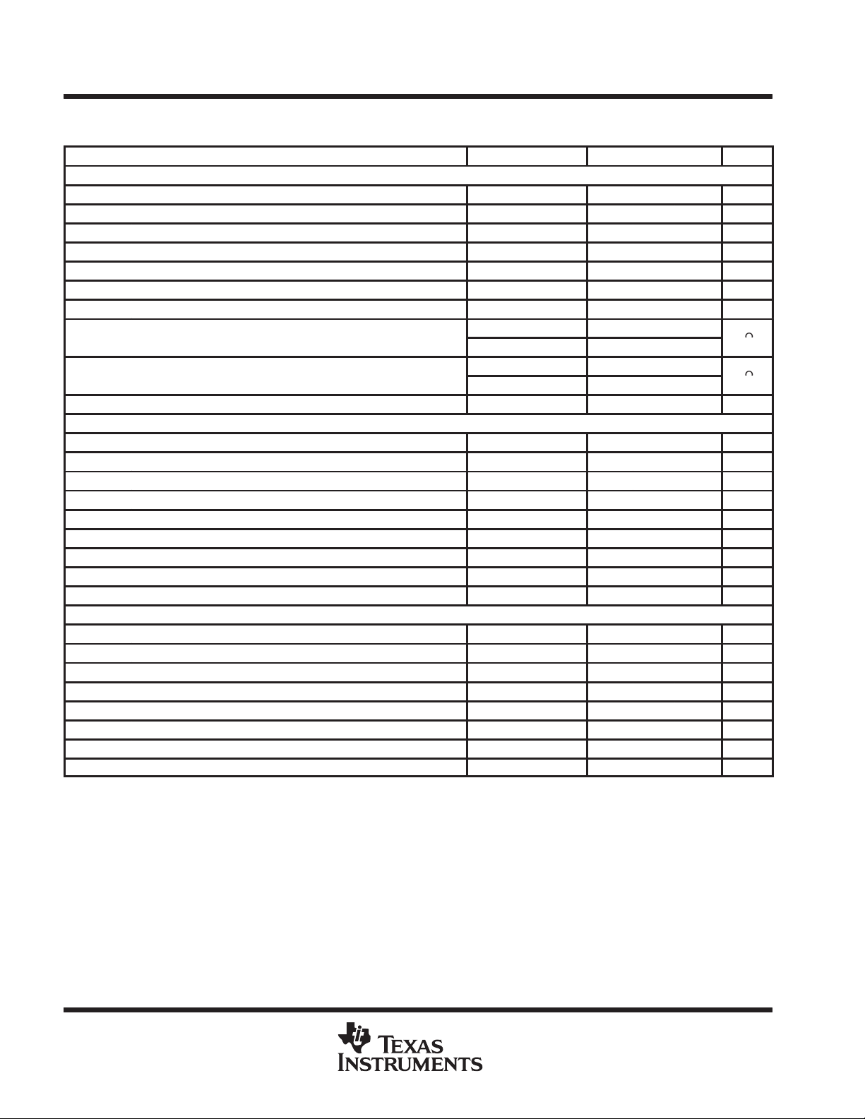
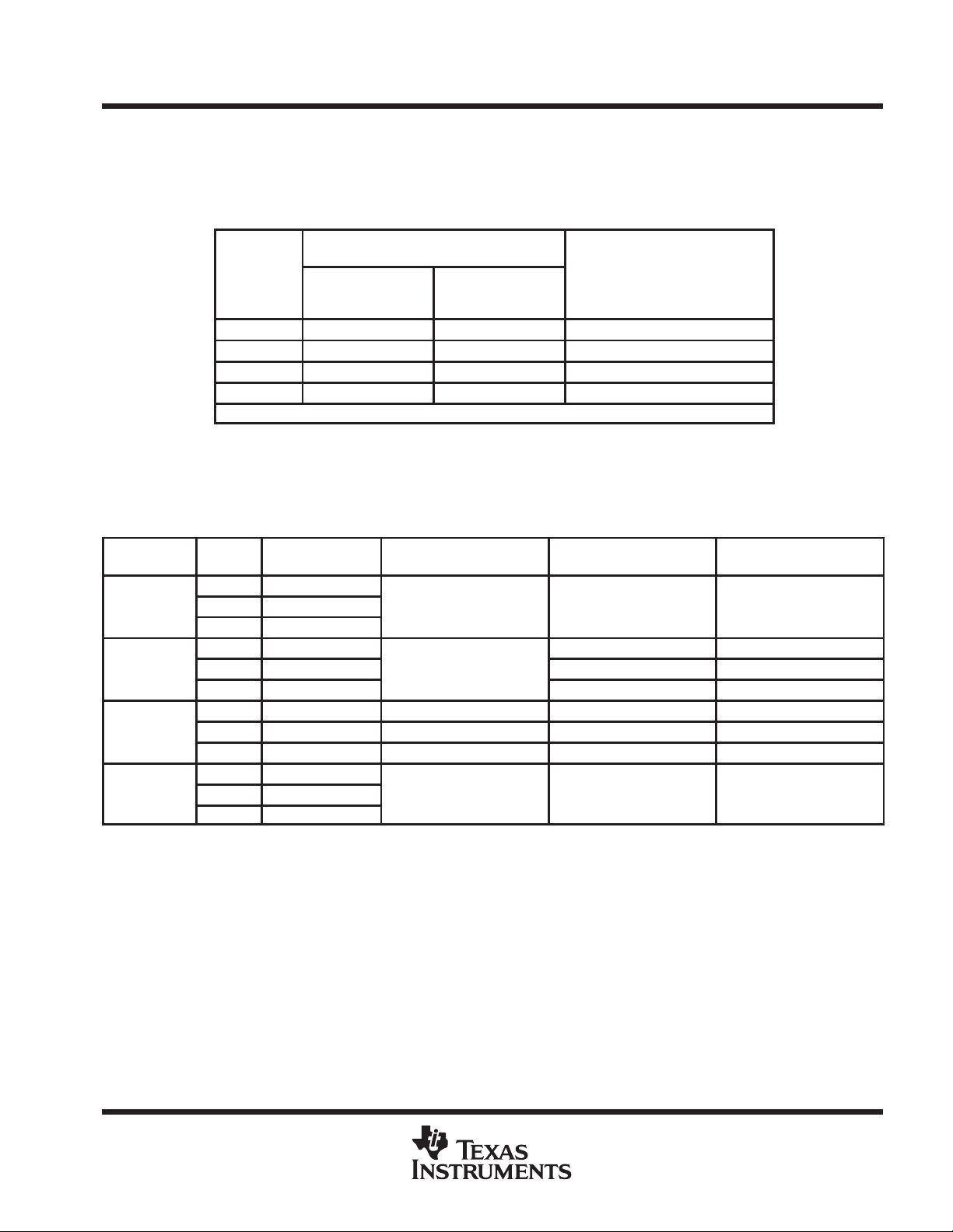
electrical characteristics, A VDD = 5 V , DVDD = 3.3 V , GND = 0 V, TA = 0°C to 70°C (unless otherwise
noted)
PARAMETER TEST CONDITIONS MIN TYP MAX UNIT
Digital Logic Levels (DVDD = 3.3 V or 5 V)
V
IL
V
IH
V
OL
V
OH
Analog I/O Levels (input signals on any inputs, outputs on LINEOUT L, R, and MONOOUT)
Reference Levels
CAP2 Reference input/output 2/5 AV
VREF Mixer reference
VREFOUT MIC reference
CAP1 ADC reference
AFILT1 DAC reference
DAC Circuit Specifications (AVDD = 5 V) 48-kHz sampling
ADC Circuit Specifications (AVDD = 5 V) 48-kHz sampling
NOTE 1: SNR is the ratio of 0-dB signal output level to the output level with no signal, measured A-weighted over a 20 Hz to 20 kHz bandwidth.
Input low level AVSS – 0.3 0.8 V
Input high level 2.2 AVDD + 0.3 V
Output low 0.1 × DV
Output high 0.9 × DV
Input level
Output level Into 10 kΩ load AVSS +100 mV
CAP2 impedance 75 kΩ
VREF current source (pins CAP1, AFILT2,
VREF and VREFOUT)
VREF current source (pins CAP1, AFILT1,
VREF and VREFOUT)
SNR A-weighted (see Note 1) 85 95 dB
Full-scale output voltage VREF = 2.5 V 1 Vrms
THD –3-dB full-scale input 74 96 dB
Frequency response 20 19200 Hz
Transition band 19200 28800 Hz
Stop band 28800 Hz
Out of band rejection –40 dB
Spurious-tone reduction –100 dB
PSRR 20 Hz to 20 kHz 40 dB
SNR A-weighted (see Note 1) 75 90 dB
ADC input for full-scale output VREF = 2.5 V 1 Vrms
THD –6-dB voltage input 80 95 dB
Frequency response 20 19200 Hz
Transition band 19200 28800 Hz
Stop band 28800 Hz
Stop-band rejection –74 dB
PSRR 20 Hz to 20 kHz 40 dB
Minimum input
impedance = 10 kΩ
AVDD = 3 V 5 15 mA
AVDD = 5 V 3 5 mA
AVSS –100 mV AVDD +100 mV V
DD
Near rail
to rail
AVDD/2 3/5 AV
DD
Buffered
CAP2
Buffered
CAP2
Buffered
CAP2
Buffered
CAP2
AVDD –100 mV V
DD
DD
V
V
V
V
V
V
V
POST OFFICE BOX 655303 • DALLAS, TEXAS 75265
7
Page 8
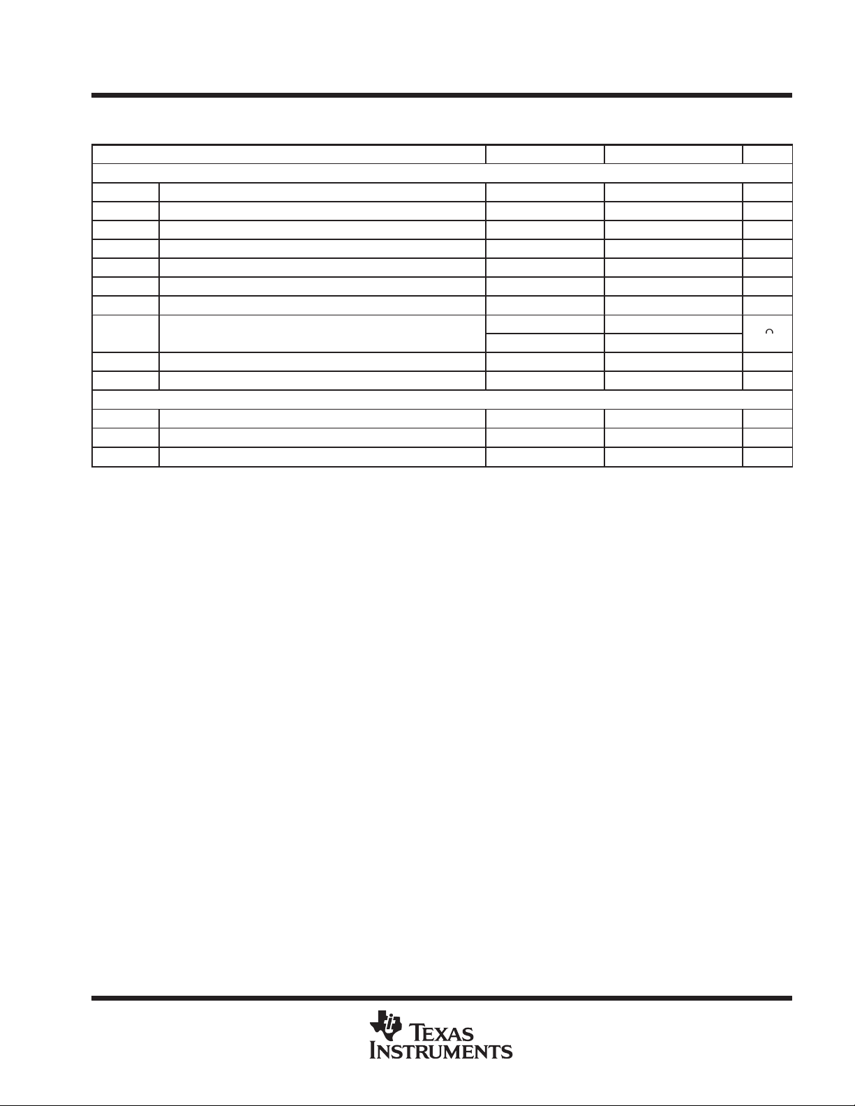
TLV320AIC27
Input impedance (other mixer inputs)
kΩ
Input impedance mic inputs
kΩ
STEREO AUDIO CODEC
SLAS253 – MARCH 2000
electrical characteristics, A VDD = 5 V , DVDD = 3.3 V , GND = 0 V, TA = 0°C to 70°C (unless otherwise
noted) (continued)
PARAMETER TEST CONDITIONS MIN TYP MAX UNIT
Mixer Circuit Specifications (AVDD = 5 V) 48-kHz sampling
SNR CD path A-weighted (see Note 1) 90 95 dB
SNR other paths A-weighted (see Note 1) 85 95 dB
Maximum input voltage AV
Maximum output voltage on LINEOUT 1.0 1.8 Vrms
THD 0-dB voltage input 74 90 dB
Frequency response (±1 dB) 20 20000 Hz
Input impedance (CD inputs) At any gain 15 kΩ
p
p
p
p
PSRR 20 Hz to 20kHz 40 dB
DAC Circuit Specifications (AVDD = 3.3 V) 48-kHz sampling
SNR A-weighted (see Note 1) 96 dB
Full scale output voltage VREF = 1.65 V 0.7 Vrms
THD –3-dB full-scale input 66 90 dB
Frequency response 20 Hz
Transition band 19200 19200 Hz
Stop band 28800 28800 Hz
Out-of-band rejection –40 dB
Spurious-tone reduction –100 dB
PSRR 20 Hz to 20 kHz 40 dB
ADC-Circuit Specifications (AVDD = 3.3 V) 48-kHz sampling
SNR A-weighted (see Note 1) 85 dB
ADC input for full-scale output VREF = 1.65 V 0.7 Vrms
THD –6-dB voltage input 74 80 dB
Frequency response 20 19200 Hz
Transition band 19200 28800 Hz
Stop band 28800 Hz
Stop-band rejection –74 dB
PSRR 20 Hz to 20 kHz 40 dB
NOTE 1: SNR is the ratio of 0-dB signal output level to the output level with no signal, measured A-weighted over a 20 Hz to 20 kHz bandwidth.
p
p
At maximum gain 10 20 30
At 0-db gain 50 100 150
At maximum gain 10 20 30
At 0-db gain 55 110 165
SS
1 AV
DD
Vrms
8
POST OFFICE BOX 655303 • DALLAS, TEXAS 75265
Page 9
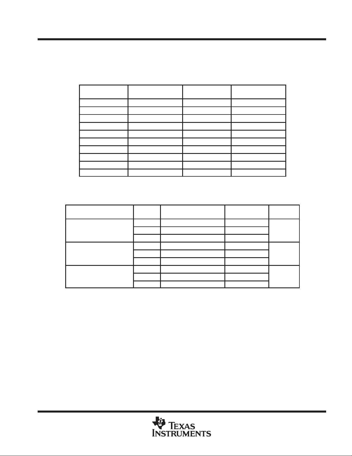
Input impedance (other mixer inputs)
kΩ
TLV320AIC27
STEREO AUDIO CODEC
SLAS253 – MARCH 2000
electrical characteristics, A VDD = 5 V , DVDD = 3.3 V , GND = 0 V, TA = 0°C to 70°C (unless otherwise
noted) (continued)
PARAMETER TEST CONDITIONS MIN TYP MAX UNIT
Mixer-Circuit Specifications (AVDD = 3.3 V) 48 kHz sampling
SNR CD path A-weighted (see Note 1) 92 dB
SNR other paths A-weighted (see Note 1) 92 dB
Maximum input voltage 0.66 Vrms
Maximum output voltage on LINEOUT 0.66 Vrms
THD 0-dB voltage input 74 90 dB
Frequency response (±1 dB) 20 20000 Hz
Input impedance (CD inputs) At any gain 15 kΩ
p
p
Input impedance mic inputs At any gain 30 kΩ
PSRR 20 Hz to 20 kHz 40 dB
Clock-Frequency Range
Crystal clock 24.576 MHz
BIT_CLK frequency 12.288 MHz
SYNC frequency 48.0 kHz
NOTE 1: SNR is the ratio of 0-dB signal output level to the output level with no signal, measured A-weighted over a 20 Hz to 20 kHz bandwidth.
p
At maximum gain 20
At 0-dB gain 100
POST OFFICE BOX 655303 • DALLAS, TEXAS 75265
9
Page 10

TLV320AIC27
STEREO AUDIO CODEC
SLAS253 – MARCH 2000
detailed description
3D stereo enhancement
This device contains a stereo-enhancement circuit, designed to optimize the listening experience when the
device is used in a typical PC-operating environment (that is, with a pair of speakers placed either side of the
monitor with little spatial separation). This circuit creates a differential signal by subtracting left and right channel
playback data, then filters this difference signal using low-pass and high-pass filters whose time constants are
set using external capacitors connected to the CX3D pins 33 and 34. Typical values of 100 nF and 47 nF set
high-pass and low-pass poles at about 100 Hz and 1 kHz respectively . This frequency band corresponds to the
range over which the ear is most sensitive to directional effects.
The filtered difference signal is gain-adjusted by an amount set using the four-bit value written to register 22h
bits 3 to 0. Value 0h is disabled, and value Fh is maximum effect. A typical value of 8h is optimum. The user
interface most typically uses a slider type of control to allow the user to adjust the level of enhancement to suit
the program material. Bit D13 3D in register 20h is the overall 3D-enable bit. The capability register 00h reads
back the value 1 1000 in bits D14 to D10. This corresponds to decimal 24, which is registered with Intel as T exas
Instruments Stereo Enhancement.
Note that the external capacitors setting the filtering poles applied to the difference signal can be adjusted in
value, or even replaced with a direct connection between the pins. When such adjustments are made, the
amount of difference signal fed back into the main signal paths can be significant. This can cause large signals
which may limit, distort, or overdrive signal paths or speakers. Adjust these values carefully to select the desired
acoustic effect.
There is no provision for pseudo-stereo effects. Mono signals have no enhancement applied if they are in phase
and have the same amplitude.
Signals from the PCM DAC channels do not have stereo enhancement applied. It is assumed that these signals
have already been processed digitally with any required 3D-enhancement effect. Applying the analog
3D-enhancement will corrupt the digital effect. This is equivalent to setting the POP bit in register 20h. As a
result, the readback value of this bit is fixed as 1, and attempts to change it will be ignored. The POP bit is set
to one and cannot be reset.
variable sample rate support
The DACs and ADCs on this device support all the recommended sample rates specified in the Intel Revision
2.1 specification for both audio and modem rates. Default rates are 48 ksps. If alternative rates are selected,
the AC’97 interface continues to run at 48 kw/s (kilowords per second), but data is transferred across the link
in bursts such that the net sample rate selected is achieved. It is up to the AC’97 Revision 2.1-compliant
controller to ensure that data is supplied to the ac link, and received from the ac link at the appropriate rate.
The device supports on-demand sampling. That is, when the DAC signal-processing circuits need another
sample a request is sent to the controller, which must respond with a data sample in the next frame it sends.
For example, if a rate of 24 ksps is selected, on average the device requests a sample from the controller every
other frame, for each of the stereo DACs. Note that if an unsupported rate is written to one of the rate registers,
the rate defaults to the nearest rate supported. The register then responds when interrogated with the supported
rate the device has defaulted to.
10
POST OFFICE BOX 655303 • DALLAS, TEXAS 75265
Page 11
TLV320AIC27
STEREO AUDIO CODEC
SLAS253 – MARCH 2000
variable sample rate support (continued)
ADCs are controlled similarly but with one difference: normally the left and right-channel ADCs sample at the
same rate.
Table 1. Variable Sample Rates Supported
AUDIO
SAMPLE RATE
8000 1F40 7200 1C20
11025 2B11 8228.57 (57600/7) 2024
16000 3E80 8400 20D0
22050 5622 9000 2328
44100 AC44 9600 2580
48000 BB80 10285.71 (72000/7) 282D
CONTROL VALUE
D15–D0
MODEM
SAMPLE RATE
12000 2EE0
13714.28 (96000/7) 3592
19200 4B00
24000 5DC0
CONTROL VALUE
D15–D0
Table 2 shows which registers control which DAC rates, versus mode and ID selected.
Table 2. Variable Rate Register Location Versus Mode and ID
MODE ID
Rev 2.1 mode (00)
Rev 2.1 6-channel mode (01)
Quad mode (10)
FRONT DAC RATE
REGISTER
00 and 01 2Ch
10 2Eh
11 2Ch (center) and 30h (LFE)
00 and 01 2Ch
10 2Eh
11 2Ch (center) and 30h (LFE)
00 and 01 2Ch 2Eh
10 2Eh 2Ch
11 2Ch (center) and 30h (LFE) 2Eh
REAR DAC RATE
REGISTER
ADC RATE
REG
32h
32h
32h
gain control register location versus mode and ID
Depending on the operational mode and ID of the device, the various gain control registers have locations in
the register map that may change. For example, if the codec is configured as ID 10, it means that the device
will be converting the rear surround DAC data. In this case, the surround DAC volume word written to register
38h is now used to control the master volume control, rather than the normal master volume 02h. In addition,
when the surround volume mute control is written as demute, mute in the DAC PGA register 18h is automatically
overridden. Then the user does not have to make an unexpected additional write to register 18h to demute the
DAC PGA.
POST OFFICE BOX 655303 • DALLAS, TEXAS 75265
11
Page 12
TLV320AIC27
STEREO AUDIO CODEC
SLAS253 – MARCH 2000
gain control register location versus mode and ID (continued)
Table 3. Gain Control Register Location Versus Mode and ID
PGA
Front DAC PGA
Rear DAC PGA
Front mixer
Rear mixer
Front volume
Rear volume
CODECIDCONTROL
0x
10
11
0x
10
11
0x
10
11
0x
10
11
0x
10
11
0x
10
11
REG
18h
70h
72h Not muted (bit 15) Not muted (bit 15) Not muted (bit 15)
74h Permanently muted Not muted (bit 15) Permanently muted
02h
38h
36h
04h
REV 2.1 MODE (0x)
MUTE DEFAULT
Muted (bit 15)
AND with 38h, 7, 15
AND with 36h, 7, 15
Muted (bit 15) and
powered off
Muted (bit 15)
Muted (7 and 15)
Muted (7 and 15)
Muted (bit 15) Rev 2.1
switch enabled
QUAD MODE (10)
MUTE DEFAULT
Muted (bit 15)
AND with 38h, 7, 15
AND with 36h, 7, 15
Not muted (bit 15)
AND with 02h, 15
AND with 38h, 7, 15
Muted (bit 15)
Muted (7 and 15)
Muted (7 and 15)
Muted (7 and 15)
Muted (bit 15)
Muted (7 and 15)
MODEM MODE (11)
Muted (bit 15)
AND with 38h, 7, 15
AND with 36h, 7, 15
AND with 04h, 15
Muted (bit 15)
Muted (7 and 15)
Muted (7 and 15)
Muted (bit 15)
master/slave ID0/1 support
TL V320AIC27 supports operation as either a master or a slave codec. Configuring the device as master or slave
is accomplished by tying together the CID pins CID0 and CID1 (pins 45 and 46 ).
Fundamentally , a device identified as a master (ID = 00) produces BITCLK as an output, whereas a slave (any
ID but 00) must be provided with BITCLK as an input. The obvious implication is that if the master device on
an ac link is disabled, the slave devices cannot function.
The AC’97 Revision 2.1 specification defines the CID pins as having inverting sense and being provided with
internal weak pull ups. Therefore, if no connections are made to the CID0/1 pins, then these pins pull hi and
an ID = 00 (or master) is selected. External connections to ground select other IDs.
Table 4. ID Selection
PIN 45 CID0 PIN 46 CID1 ID SELECTED
NC NC 00 Master Output
NC Ground 01 Slave Input
Ground NC 10 Slave Input
Ground Ground 11 Slave Input
MASTER OR
SLAVE
BITCLK
12
POST OFFICE BOX 655303 • DALLAS, TEXAS 75265
Page 13
6-channel (01)
TLV320AIC27
STEREO AUDIO CODEC
SLAS253 – MARCH 2000
master/slave ID0/1 support (continued)
The TL V320AIC27 supports the AMAP function, whereby selection of an ID automatically maps the data from
the interface onto the PCM DACs.
Table 5. Default Slot to DAC Mappings Based on Codec ID
AC-LINK FRAME DATA
USED FOR DACs
CODEC ID
00 3 4 Original definition (master)
01 3 4 Original definition (docking)
10 7 8 Left/right surround channels
11 6 9 Center/LFE channels
The codec ID is available to the controller via register 28h and C3, bits D15 and D14
PCM LEFT DAC
USES DATA FROM
SLOT NUMBER
PCM RIGHT DAC
USES DATA FROM
SLOT NUMBER
The previous automatic mapping of data to slots is extended when the device is operated in the alternative
modes selectable via the mode pins. In these cases the selection of which data slots are mapped onto internal
DACs or I2S outputs is accomplished as shown in Table 6. Note that I2S enable bit must be set.
COMMENTS
Table 6. Slot to DAC and Mapping Based on Mode and Codec ID
MODE
Rev 2.1 (00)
Rev 2.1
-
Quad (10)
Modem (11)
CODECIDSLOTS MAPPED
TO FRONT DACs
00 or 01 3 and 4
10 7 and 8
11 6 and 9
00 or 01 3 and 4 7 and 8 6 and 9
10 7 and 8
11 6 and 9 7 and 8 3 and 4
00 or 01 3 and 4 7 and 8 7 and 8 6 and 9
10 7 and 8 3 and 4 3 and 4 6 and 9
11 6 and 9 7 and 8 7 and 8 3 and 4
00 or 01 3 and 4
10 7 and 8
11 6 and 9
SLOTS MAPPED TO
REAR DACs
Not supported in this mode Not supported in this mode Not supported in this mode
Not supported in this mode
5 (or 5 and 10 if DLM set) Not supported in this mode Not supported in this mode
DATA TO I2S D0
PIN 44
3 and 4 6 and 9
DATA TO I2S D1
PIN 43
slave codec register access definitions
Master codec access is exactly as defined for AC’97. For slave codec access, the AC’97 digital controller must
invalidate the tag bits for slots 1 and 2 command address and data (slot 0, bits 14 and 13) and place a nonzero
value (01, 10, or 11) into the codec ID field (slot 0, bits 1 and 0).
Slave codecs disregard the command address and command data (slot 0, bits 14 and 13) tag bits when they
see a two-bit codec ID value (slot 0, bits 1 and 0) that matches their configuration. In a sense, the slave codec
ID field functions as an alternative valid command address (for slave reads and writes) and command data (for
slave writes) tag indicator.
Slave codecs must monitor the frame valid bit and ignore the frame (regardless of the state of the slave codec
ID bits) when it is not valid. AC’97 digital controllers should set the frame valid bit for a frame with a slave register
access, even if no other bits in the output tag slot, except the slave codec ID bits, are set.
POST OFFICE BOX 655303 • DALLAS, TEXAS 75265
13
Page 14
TLV320AIC27
STEREO AUDIO CODEC
SLAS253 – MARCH 2000
slave codec register access definitions (continued)
Table 7. Slave Codec Register Access Slot 0 – Bit Definitions
OUTPUT TAG SLOt (16 bits)
BIT DESCRIPTION
15 Frame valid
14 Slot 1 valid command address bit (master codec only)
13 Slot 2 valid command data bit (master codec only)
12–3 Slot 3–12 valid bits as defined by AC’97
2 Reserved (set to 0)
1–0 Two-bit codec ID field (00 reserved for master; 01, 10, 11 indicate slave)
New definitions for slave codec register access
control interface
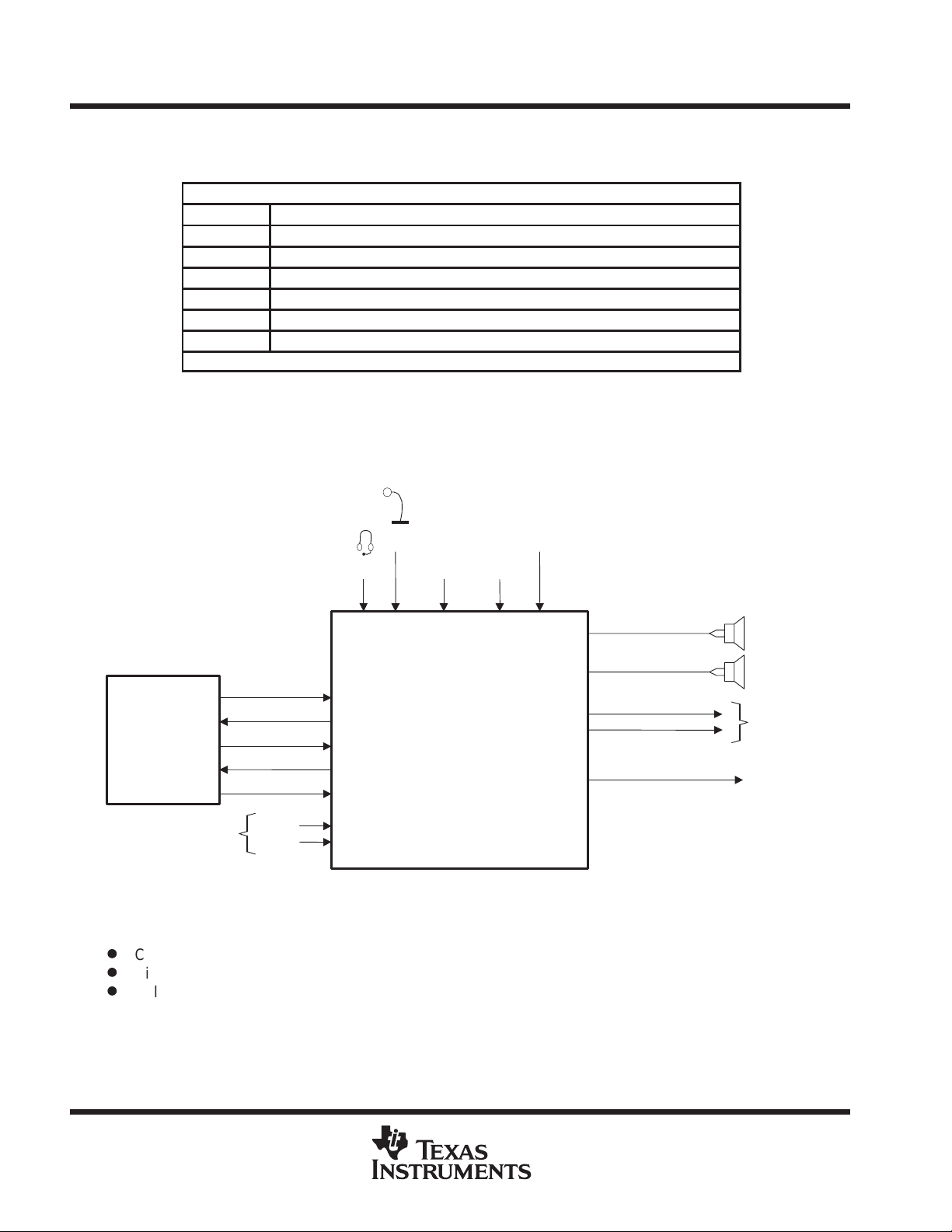
A digital interface is provided to control the TL V320AIC27 and transfer data to and from it. This serial interface
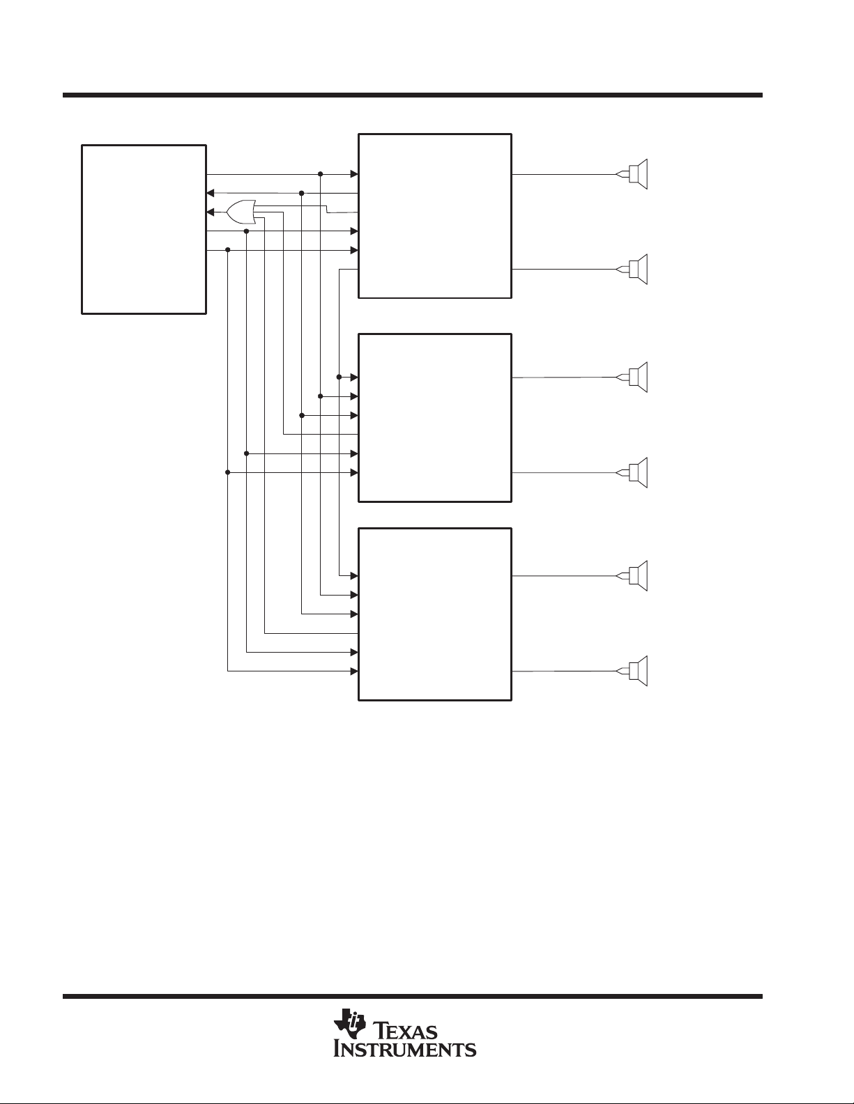
is compatible with the Intel AC’97, as illustrated in Figure 1.
system information
CD, VIDEO,
AUX, LINEINL/R
13122122
35
36
39
41
37
C54X
/C6X
OR AC’97
COMPLIANT
DIGITAL
CONTROLLER
SELECT
CHIP
RESET
BITCLK
SYNC
SDATAIN
SDATAOUT
CID0
CID1
11
6
10
8
5
45
46
MIC2
MIC1
PCBEEP PHONE
TLV320AIC27
Figure 1. Revision 2.1 Compliant Two-Channel Codec
The main control interface functions are:
D
Control of analog gain and signal paths through the mixer
D
Bidirectional transfer of ADC and DAC words to and from AC’97 controller
D
Selection of power down modes
LINEOUTL/R
LNLVLOUTL/R
MONOOUT
14
POST OFFICE BOX 655303 • DALLAS, TEXAS 75265
Page 15
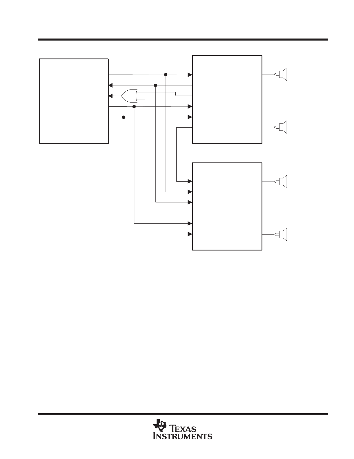
system information (continued)
TLV320AIC27
STEREO AUDIO CODEC
SLAS253 – MARCH 2000
TLV320AIC27
SDATAOUT
C54XX/C6X
McBSP
Or AC’97 compliant
digital controller
BITCLK
SDATAIN
SYNC
RESET
SDATAOUT
BITCLK
SDATAIN
SYNC
RESET
XTLOUT
TLV320AIC27
XTLIN
SDATAOUT
BITCLK
SDATAIN
SYNC
RESET
LINEOUTL
LINEOUTR
ID=00
LINEOUTL
LINEOUTR
ID=10
Front R data
Front L data
Surround R data
Surround L data
Figure 2. TLV320AIC27 In a Four-Channel System
POST OFFICE BOX 655303 • DALLAS, TEXAS 75265
15
Page 16
TLV320AIC27
STEREO AUDIO CODEC
SLAS253 – MARCH 2000
system information (continued)
TLV320AIC27
C54XX
C6X
McBSP
SDATAOUT
SDATAIN
OR AC’97
COMPLIANT
DIGITAL
CONTROLLER
BITCLK
SYNC
RESET
SDATAOUT
BITCLK
SDATAIN
SYNC
RESET
XTLOUT
TLV320AIC27
XTLIN
SDATAOUT
BITCLK
SDATAIN
SYNC
RESET
TLV320AIC27
XTLIN
SDATAOUT
BITCLK
SDATAIN
SYNC
RESET
LINEOUTL
LINEOUTR
ID=00
LINEOUTL
LINEOUTR
ID=10
LINEOUTL
LINEOUTR
ID=11
Front R data
Front L data
Surround R data
Surround L data
Center data
LFE data
16
Figure 3. TLV320AIC27 In a Six-Channel System
POST OFFICE BOX 655303 • DALLAS, TEXAS 75265
Page 17

system information (continued)
MIC2
MIC1
PCBEEP PHONE
TLV320AIC27
STEREO AUDIO CODEC
SLAS253 – MARCH 2000
CD, VIDEO,
AUX, LINEINL/R
C54X
/C6X
OR AC’97
COMPLIANT
DIGITAL
CONTROLLER
RESET
BITCLK
SYNC
SDATAIN
SDATAOUT
CHIP
SELECT
CID0
CID1
11
6
10
8
5
45
46
AIC27
(Quad Mode)
13122122
43
GPIO
35
36
39
41
37
48
[1:3]
I2S Data
LRCLK
BITCLK
SCLK
Figure 4. AIC27 In Typical Quad-Mode Application
MONOOUT
Optional For AC-3 Type
Surround Sound (5.1)
External
DAC
LINEOUTL/R
Front Data
LNLVLOUTL/R
Rear Data
Surround
Sound
(Center and
LFE Data)
POST OFFICE BOX 655303 • DALLAS, TEXAS 75265
17
Page 18

TLV320AIC27
STEREO AUDIO CODEC
SLAS253 – MARCH 2000
system information (continued)
MIC2
MIC1
PCBEEP PHONE
CD, VIDEO,
AUX, LINEINL/R
C54X
/C6X
OR AC’97
COMPLIANT
DIGITAL
CONTROLLER
CHIP
SELECT
RESET
BITCLK
SYNC
SDATAIN
SDATAOUT
CID0
CID1
11
6
10
8
5
45
46
23
XTAL
AIC27
(Modem Mode)
MODE0 = 1
MODE1 = 1
13122122
GPIO [1:3]
35
36
39, 41
13
37
484443
LNLVL_OUT_L/R
Phone
MONOOUT
Figure 5. AIC27 In a Typical Modem Application
Tx
Rx
LINE_OUT_L/R
Front Data
DAA
Modem
Data
18
POST OFFICE BOX 655303 • DALLAS, TEXAS 75265
Page 19

TLV320AIC27
STEREO AUDIO CODEC
SLAS253 – MARCH 2000
ac-link digital serial interface protocol
The TL V320AIC27 incorporates a five-pin digital serial interface that links it to the AC’97 controller . The ac link
is a bidirectional, fixed rate, serial PCM digital stream. It handles multiple input and output audio streams, as
well as control register-accesses employing a time-division multiplexed (TDM) scheme. The ac-link architecture
divides each audio frame into 12 outgoing and 12 incoming data streams, each with 20-bit sample resolution.
With a minimum required resolution of 16-bits for the DAC and the ADC, AC’97 can also be implemented with
18 or 20-bit DAC/ADC resolution, given the headroom that the ac-link architecture provides. The TL V320AIC27
provides support for 18-bit operation.
SLOT
NUMBER
SYNC
SDATA_OUT
SDATA_IN
0123456789101112
CMD
CMD
PCM
CODEC ID
SLOTREQ 3–12
TAG
TAG
ADR
STATUS
ADDR
DATA
STATUS
DATA
LEFT
PCM
LEFT
PCM
RSRVD
RIGHT
PCM
RSRVD RSRVD RSRVD RSRVD RSRVD RSRVD RSRVD
RIGHT
PCM
CENTER
PCM
L SURR
R SURR
PCM
PCM
LFE
RSRVD RSRVD
PCM L
(n+1)
PCM R
(n+1)
GPIO
CTRL
PCM C
(n+1)
GPIO
STATUS
TAG PHASE
Figure 6. AC’97 Standard Bidirectional Audio Frame Basic Mode (Two-Channel)
SLOT
NUMBER
SYNC
SDATA_OUT
SDATA_IN
TAG PHASE
DATA PHASE
0123456789101112
LFE
LINE 2
DAC
PCM L
(n+1)
LINE 2
DAC
CODEC ID
SLOTREQ 3–12
TAG
TAG
CMD
ADR
STATUS
ADDR
CMD
DATA
STATUS
DATA
PCM
LEFT
PCM
LEFT
PCM
LINE 1 PCM
RIGHT
PCM
LINE 1
RIGHT
PCM
DAC
CENTER
RSRVD RSRVD RSRVD RSRVD RSRVD
DAC
PCM
L SURR
PCM
R SURR
DATA PHASE
Figure 7. AC’97 Standard Bidirectional Audio Frame Modem Mode
RSRVD
PCM R
(n+1)
GPIO
CTRL
PCM C
(n+1)
GPIO
STATUS
POST OFFICE BOX 655303 • DALLAS, TEXAS 75265
19
Page 20

TLV320AIC27
STEREO AUDIO CODEC
SLAS253 – MARCH 2000
ac-link digital serial interface protocol (continued)
SLOT
NUMBER
SYNC
SDATA_IN
0123456789101112
CMD
CMD
PCM
LEFT
PCM
LEFT
PCM
RIGHT
PCM
RIGHT
CODEC ID
SLOTREQ 3–12
TAG
TAG
ADR
STATUS
ADDR
DATA
STATUS
DATA
Figure 8. AC’97 Standard Bidirectional Audio Frame In Quad Mode
LINE 1
LINE 1
PCM
CENTER
DAC
MIC
DAC ADC
20.8 µS (48 kHz)
PCM
PCM
LFE
PCM
L SURR
R SURR
RSRVD RSRVD RSRVD
DATA PHASETAG PHASE
LINE 2
DAC DAC
PCM R
PCM L
(n+1)
ADC ADC
HSET
(n+1)
HSETLINE 2
IO
CTRL
PCM C
(n+1)
IO
STATUS
SYNC
12.288 MHz
81.4 nS
BIT_CLK
SDATA_OUT
END OF PREVIOUS
AUDIO FRAME
SLOT(1) SLOT(2) SLOT(12)
FRAME
TIME SLOT ’VALID’ BITS
(’1’ = TIME SLOT CONTAINS
VALID PCM DATA)
’0’ ’0’ ’0’ 19 0 19 0 19 0 19 0
SLOT (1) SLOT (2) SLOT (3) SLOT (12)
VALID
Figure 9. AC-Link Serial Interface Protocol Output Frame
The data streams currently defined by the AC’97 specification include:
PCM playback—two output slots Two-channel composite PCM output stream
PCM record data—two input slots Two-channel composite PCM input stream
Control—two output slots Control register write port
Status—two input slots Control register read port
Optional dedicated microphone input—one input slot
Optional modem line codec output—one output slot Modem line codec DAC input stream
Optional modem line codec input—one input slot Modem line codec ADC output stream
Dedicated microphone input stream in support of stereo AEC
and/or other voice applications
The TL V320AIC27 controller signals synchronization of all ac-link data transactions. The TL V320AIC27 drives
the serial bit clock onto the ac link, which the AC’97 controller then qualifies with a synchronization signal to
construct audio frames.
SYNC, fixed at 48 kHz, is derived by dividing down the serial clock (BIT_CLK). BIT_CLK, fixed at 12.288 MHz,
provides the necessary clocking granularity to support 12 20-bit outgoing and incoming time slots. Ac-link serial
data transition occurs on each rising edge of BIT_CLK. The receiver of ac-link data (TL V320AIC27 for outgoing
data and AC’97 controller for incoming data) samples each serial bit on the falling edges of BIT_CLK.
20
POST OFFICE BOX 655303 • DALLAS, TEXAS 75265
Page 21

TLV320AIC27
STEREO AUDIO CODEC
SLAS253 – MARCH 2000
ac-link digital serial interface protocol (continued)
The ac-link protocol provides for a special 16-bit time slot (slot 0) wherein each bit conveys a valid tag for its
corresponding time slot within the current audio frame. A 1 in a given bit position of slot 0 indicates that the
corresponding time slot within the current audio frame has been assigned to a data stream and contains valid
data. If a slot is tagged invalid, it is the responsibility of the data source (the TL V320AIC27 for the input stream
and the AC’97 controller for the output stream) to fill all bit positions with 0s during that slot’s active time.
SYNC remains high for a total duration of 16 BIT_CLKs at the beginning of each audio frame.
The portion of the audio frame where SYNC is high is defined as the tag phase. The remainder of the audio frame
where SYNC is low is defined as the data phase. Additionally, all clock, sync, and data signals can be halted
to save power. This requires that the TLV320AIC27 be implemented as a static design to allow its register
contents to remain intact when entering a power savings mode.
ac-link audio output frame (SDATA_OUT)
The audio output frame data streams correspond to the multiplexed bundles of all digital output data targeting
the TL V320AIC27’s DAC inputs and control registers. As mentioned earlier, each audio output frame supports
up to 12 20-bit outgoing data time slots. Slot 0 is a reserved time slot containing 16-bits, which are used for
ac-link protocol infrastructure.
The first bit within slot 0 is a global bit (SDA TA_OUT slot 0, bit 15) which flags the validity for the entire audio
frame. A valid frame bit equal to 1 indicates that the current audio frame contains at least one time slot of valid
data. The next 12-bit positions sampled by the TL V320AIC27 indicate which of the corresponding 12 time slots
contain valid data.
In this way , data streams of differing sample rates can be transmitted across the ac link at its fixed 48-kHz audio
frame rate. Figure 9 illustrates the time-slot-based ac-link protocol.
AIC27 SAMPLES
SYNC ASSERTION HERE
SYNC
AIC27 SAMPLES
FIRST SDATA_OUT
BIT OF FRAME HERE
BIT_CLK
SDATA_OUT
VALID
FRAME
END OF PREVIOUS AUDIO FRAME
SLOT (1) SLOT (2)
Figure 10. Start of an Audio Output Frame
A new audio output frame begins with a low-to-high transition of SYNC, as shown in Figure 10. SYNC is
synchronized to the rising edge of BIT_CLK. On the falling edge of BIT_CLK immediately following, the
TL V320AIC27 samples the assertion of SYNC. This falling edge marks the time when both sides of the ac link
are aware of the start of a new audio frame. On the next rising edge of BIT_CLK, AC’97 transitions SDA TA_OUT
into the first bit position of slot 0 (valid frame bit). Each new bit position is presented to the ac link on a rising
edge of BIT_CLK, and subsequently sampled by the TL V320AIC27 on the following falling edge of BIT_CLK.
This sequence ensures that data transitions and subsequent sample points for both incoming and outgoing data
streams are time-aligned.
POST OFFICE BOX 655303 • DALLAS, TEXAS 75265
21
Page 22

TLV320AIC27
STEREO AUDIO CODEC
SLAS253 – MARCH 2000
ac-link audio output frame (SDATA_OUT) (continued)
Baseline AC’97-specified audio functionality should always convert the sample rate to and from a fixed 48 ksps
on the AC’97 controller. This requirement ensures that interoperability between the AC’97 controller and the
TLV320AIC27, among other things, can be assured by definition for baseline specified AC’97 features.
SDATA_OUT’s composite stream is MSB justified (MSB first), with all invalid slot bit positions stuffed with 0s
by the AC’97 controller. In the event that there are less than 20 valid bits within an assigned and valid time slot,
the AC’97 controller always stuffs all trailing invalid bit positions of the 20-bit slot with 0s.
As an example, consider an eight-bit sample stream that is being played out to one of the TL V320AIC27’s DACs.
The first eight-bit positions are presented to the DAC (MSB justified), followed by the next 12-bit positions, which
are stuffed with 0s by the AC’97 controller . This ensures that, regardless of the resolution of the implemented
DAC (16, 18, or 20-bit), no dc biasing is introduced by the least significant bits. When mono audio sample
streams are outputted from the AC’97 controller, it is necessary that
be filled with the same data.
slot 1: command address port
The command port is used to control features and monitor status for the TL V320AIC27 functions including, but
not limited to, mixer settings and power management (refer to the serial interface register map). The control
interface architecture supports up to 64 16-bit read/write registers, addressable on even-byte boundaries. Only
the even registers (00h, 02h, etc.) are valid. Access to odd registers (01h, 03h, etc.) is discouraged (if supported,
they should default to the preceding even-byte boundary—that is, a read from 01h returns the 16-bit contents
of 00h). The TL V320AIC27’ s control register file is nonetheless readable as well as writeable to provide more
robust testability.
both
left and right sample-stream time slots
Audio output frame slot 1 communicates control register address and read/write command information to the
TLV320AIC27.
Command Address Port Bit Assignments
Bit (19)
Bit (18:12) Control register index (64 16-bit locations, addressed on even byte boundaries)
Bit (11:0) Reserved (stuffed with 0s)
Read/write command (1 = read, 0 = write)
The first bit (MSB) sampled by the TL V320AIC27 indicates whether the current control transaction is a read or
a write operation. The following seven bit positions communicate the targeted control register address. The
trailing 12 bit positions within the slot are reserved and must be stuffed with 0s by the AC’97 controller.
slot 2: command data port
The command data port is used to deliver 16-bit control register write data in the event that the current command
port operation is a write cycle, as indicated by slot 1, bit 19.
Bit (19:4) Control register write data (stuffed with 0s if current operation is a read)
Bit (3:0) Reserved (stuffed with 0s)
If the current command port operation is a read, then the entire time slot must be stuffed with 0s by the AC’97
controller.
slot 3: pcm playback left channel
Audio output frame slot 3 is the composite digital audio left playback stream. In a typical games compatible PC,
this slot is composed of standard PCM (.wav) output samples digitally mixed (in the AC’97 controller or host
processor) with music synthesis output samples. If a sample stream with less than 20 bits of resolution is
transferred, the AC’97 controller must stuff all trailing invalid bit positions within this time slot with 0s.
22
POST OFFICE BOX 655303 • DALLAS, TEXAS 75265
Page 23

TLV320AIC27
STEREO AUDIO CODEC
SLAS253 – MARCH 2000
ac-link audio output frame (SDATA_OUT) (continued)
slot 4: pcm playback right channel
Audio output frame slot 4 is the composite digital audio right-playback stream. In a typical games-compatible
PC, this slot is composed of standard PCM (.wav) output samples digitally mixed (on the AC’97 controller or
host processor) with music synthesis output samples.
If a sample stream with less than 20 bits of resolution is transferred, the AC’97 controller must stuff all trailing
invalid bit positions within this time slot with 0s.
slot 5: optional modem line1 codec
Audio output frame slot 5 contains the MSB-justified modem line1 DAC input data. This optional AC’97 feature
is supported in the TLV320AIC27, but only in the modem-operation mode (selected with the mode0/1 pins).
When data is written to this location, it is applied to the rear channel DACs if the modem mode is enabled. This
is determined by the AC’97 controller interrogating the TLV320AIC27 vendor ID registers. If modem mode is
disabled, the device appears not to support a modem. If the mode is enabled, the modem support flag is set.
slot 6 to 9: surround sound data
Audio output frame slots 6 to 9 are used to send surround-sound data to the extra DAC channels. These slots
are supported by TLV320AIC27 in Revision 2.1 six-channel mode and quad mode. Note that the data in the
surround-sound slots may be applied to the internal DACs, or sent out onto the GPIO pins as I
depending upon the mode and ID selected.
2
S data,
slot 10 optional modem line2 codec
Audio output frame slot 10 contains MSB-justified modem line2 DAC input data. This optional AC’97 feature
is supported by TLV320AIC27, but only when register 5Ah DLM (dual line modem) is set.
slot 11 handset DAC
Slot 11 is not supported.
slot 12: GPIO control
Data in this slot is applied to the GPIO pins if they have been enabled via the control registers. Note that only
bits 11, 12, and 13 are supported and all others are ignored.
ac-link audio input frame (SDATA_IN)
20.8 µS (48 kHz)
DATA PHASETAG PHASE
SYNC
12.288 MHz
81.4 nS
BIT_CLK
CODEC
SDATA_IN
END OF PREVIOUS
AUDIO FRAME
SLOT(1) SLOT(2) SLOT(12)
READY
TIME SLOT ’VALID’ BITS
(’1’ = TIME SLOT CONTAINS
VALID PCM DATA)
’0’ ’0’ ’0’ 19 0 19 0 19 0 19 0
SLOT (1) SLOT (2) SLOT (3) SLOT (12)
Figure 11. AC-Link Audio Input Frame
POST OFFICE BOX 655303 • DALLAS, TEXAS 75265
23
Page 24

TLV320AIC27
STEREO AUDIO CODEC
SLAS253 – MARCH 2000
ac-link audio input frame (SDATA_IN) (continued)
The audio input frame data streams correspond to the multiplexed bundles of all digital input data targeting the
AC’97 controller. As in the case of audio output frame, each ac-link audio input frame consists of 12 20-bit time
slots.
Slot 0 is a specially reserved time slot containing 16 bits, which are used for ac-link protocol infrastructure. The
first bit in slot 0 is a global bit (SDA TA_IN, bit 15) which flags whether the TLV320AIC27 is in the codec-ready
state or not. A codec-ready bit equal to 0 indicates that the TL V320AIC27 is not ready for normal operation. For
example, this is a normal condition following reset, while the TLV320AIC27’s voltage references settle. An
ac-link codec-ready indicator bit equal to 1 indicates that the ac link and the TL V320AIC27 control and status
registers are in fully-operational state. The AC’97 controller must further probe the power-down control/status
register to determine exactly which subsections, if any, are ready.
Prior to any attempts at putting the TL V320AIC27 into operation, the AC’97 controller should poll the first bit in
the audio input frame (SDATA_IN slot 0, bit 15) for an indication that the TLV320AIC27 is codec-ready.
Once the TL V320AIC27 is codec-ready, the next 12 bit positions sampled by the AC’97 controller indicate which
of the corresponding 12 time slots are assigned to input data streams and contain valid data. Figure 1 1 illustrates
the time-slot-based ac-link protocol.
There are several subsections within the TLV320AIC27 that can independently go busy/ready. It is the
responsibility of the TLV320AIC27 controller to probe more deeply into the TLV320AIC27 register file to
determine which of the TLV320AIC27 subsections are actually ready.
AIC27 SAMPLES
SYNC ASSERTION HERE
SYNC
AC ’97 CONTROLLER
SAMPLES FIRST SDATA_IN
BIT OF FRAME HERE
BIT_CLK
SDATA_IN
END OF PREVIOUS AUDIO FRAME
CODEC
READY
SLOT (1) SLOT (2)
Figure 12. Start of an Audio Input Frame
A new audio input frame begins with a low-to-high transition of SYNC, as illustrated in Figure 12. SYNC is
synchronous with the rising edge of BIT_CLK. The TL V320AIC27 samples the assertion of SYNC on the next
falling edge of BIT_CLK. This falling edge marks the time when both sides of the ac link are aware of the start
of a new audio frame. The AC’97 controller transitions SDA T A_IN into the first bit position of slot 0 (valid frame
bit) on the next rising edge of BIT_CLK. Each new bit position is presented to the ac link on a rising edge of
BIT_CLK, and subsequently sampled by the AC’97 controller on the following falling edge of BIT_CLK. This
sequence ensures that data transitions and subsequent sample points for both incoming and outgoing data
streams are time-aligned.
24
POST OFFICE BOX 655303 • DALLAS, TEXAS 75265
Page 25

TLV320AIC27
STEREO AUDIO CODEC
SLAS253 – MARCH 2000
ac-link audio input frame (SDATA_IN) (continued)
SDATA_IN’s composite stream is MSB-justified (MSB first), with all invalid bit positions (for assigned and/or
unassigned time slots) stuffed with 0’s by the TLV320AIC27. SDATA_IN is sampled on the falling edges of
BIT_CLK.
slot 1: status address port
The status port is used to monitor the status of the TL V320AIC27 functions,, including, but not limited to, mixer
settings and power management. Audio input frame slot 1 echoes the control register index, for historical
reference, so that the data is returned to slot 2 (assuming that slots 1 and 2 had been tagged valid by the
TLV320AIC27 during slot 0).
Status Address Port Bit Assignments
Bit (19)
Bit (18:12) Control register index (echo of register index for which data is being returned)
Bit (11:0) Reserved (stuffed with 0s)
The first bit (MSB) generated by the TLV320AIC27 is always stuffed with a 0. The following 7 bit positions
communicate the associated control register address, and the trailing 12 bit positions are stuffed with 0s by the
TL V320AIC27.
Reserved (stuffed with 0s)
slot 2: status data port
The status data port delivers 16-bit control register read data.
Bit (19:4) Control register read data
Bit (3:0) Reserved (stuffed with 0s)
If slot 2 is tagged invalid by the TLV320AIC27, then the entire slot is stuffed with 0s by the TLV320AIC27.
slot 3: PCM record left channel
Audio input frame slot 3 is the left channel output of the TLV320AIC27’s input mux, post-ADC.
The TLV320AIC27’s ADCs can be implemented to support 16, 18, or 20-bit resolutions. The TLV320AIC27
sends out its ADC output data (MSB first), and stuffs any trailing invalid bit positions with 0s to fill out its 20-bit
time slot.
slot 4: PCM record right channel
Audio input frame slot 4 is the right channel output of the TLV320AIC27’s input mux, post-ADC.
The TLV320AIC27’s ADCs can be implemented to support 16, 18, or 20-bit resolutions. The TLV320AIC27
sends out its ADC output data (MSB first), and stuffs any trailing invalid bit positions with 0s to fill out its 20-bit
time slot.
slot 5: optional modem line1 codec
Slot 5 is not supported.
slot 6: optional dedicated microphone record data
Audio input frame slot 6 is an optional (post-ADC) third PCM system input channel available for dedicated use
by a desktop microphone. This optional AC’97 feature is not supported by the TLV320AIC27. This can be
determined by the AC’97 controller interrogating the TLV320AIC27 vendor ID register.
slot 7 to 11: reserved
Audio input frame slots 7 to 12 are reserved for future use and are always stuffed with 0s by the TL V320AIC27.
slot 10: optional modem line2 codec
Slot 10 is not supported.
POST OFFICE BOX 655303 • DALLAS, TEXAS 75265
25
Page 26

TLV320AIC27
STEREO AUDIO CODEC
SLAS253 – MARCH 2000
ac-link audio input frame (SDATA_IN) (continued)
slot 12:
GPIO functions supported.
ac-link low-power mode
The ac-link signals can be placed in a low-power mode. When the TLV320AIC27’s power-down register 26h
is programmed to the appropriate value, both BIT_CLK and SDA TA_IN are brought to and held at a logic-low
voltage level.
BIT_CLK and SDATA_IN transition to low occurs immediately following the decode of the write to the
power-down register 26h with PR4. When the AC’97 controller driver is ready to program the ac link into its
low-power mode, slots 1 and 2 are assumed to be the only valid stream in the audio output frame. At this point
it is assumed that all sources of audio input have also been neutralized.
The AC’97 controller should also drive SYNC and SDATA_OUT low after programming the TLV320AIC27 to
this low-power, halted mode.
Once the TL V320AIC27 has been instructed to halt BIT_CLK, a special wake up protocol must be used to bring
the ac link to the active mode, since normal audio output and input frames can not be communicated in the
absence of BIT_CLK.
waking up the ac link
There are two methods to bring the ac link out of a low-power, halted mode. Regardless of the method, it is the
AC’97 controller that performs the wake-up task.
Ac-link protocol provides for a cold and a warm TLV320AIC27 reset.
The current power-down state would ultimately dictate which form of TL V320AIC27 reset is appropriate. Unless
a cold or register reset (a write to the reset register) is performed, wherein the TLV320AIC27 registers are
initialized to their default values, registers are required to keep state during all power-down modes.
Once powered down, reactivation of the ac link via reassertion of the SYNC signal must not occur for a minimum
of four audio frame times following the frame in which the power down was triggered. When the ac link powers
up, it indicates readiness via the codec-ready bit (input slot 0, bit 15).
cold TLV320AIC27 reset
A cold reset is achieved by asserting RESETB for the minimum specified time. By driving RESETB low,
BIT_CLK, and SDA T A_OUT are activated, or reactivated as the case may be, and all the TL V320AIC27 control
registers are initialized to their default power on reset values.
RESETB is an asynchronous TLV320AIC27 input.
warm TLV320AIC27 reset
A warm TL V320AIC27 reset reactivates the ac link without altering the current TLV320AIC27 register values.
A warm reset is signalled by driving SYNC high for a minimum of 1 µS in the absence of BIT_CLK.
Within normal audio frames, SYNC is synchronous to the TLV320AIC27 input. However, in the absence of
BIT_CLK, SYNC is treated as an asynchronous input used in the generation of a warm reset to the
TL V320AIC27. The TLV320AIC27 does not respond to the activation of BIT_CLK until SYNC has been sampled
low again by the TLV320AIC27. This precludes the false detection of a new audio frame.
26
POST OFFICE BOX 655303 • DALLAS, TEXAS 75265
Page 27

TLV320AIC27
STEREO AUDIO CODEC
SLAS253 – MARCH 2000
serial interface register map description (see Table 23)
The serial interface bits perform control functions described as follows (notice that the register map is fully
specified by the AC’97 specification, and this description is simply repeated below, with optional unsupported
features omitted):
reset register (index 00h)
Writing any value to this register performs a register reset, which causes all registers to revert to their default
values. Reading this register returns the ID code of the part to indicate modem support (not supported by the
TLV320AIC27) and a code for the type of 3D stereo enhancement.
The ID decodes the capabilities of the TLV320AIC27 based on the information in Table 8.
Table 8. Reset Register Function
BIT FUNCTION
ID0 Dedicated mic PCM in channel 0
ID1 Modem line codec support 0
ID2 Bass and treble control 0
ID3 Simulated stereo (mono to stereo) 0
ID4 Headphone out support 0
ID5 Loudness (bass boost) support 0
ID6 18-bit DAC resolution 1
ID7 20-bit DAC resolution 0
ID8 18-bit ADC resolution 1
ID9 20-bit ADC resolution 0
SE4...SE0 3D-stereo enhancement technique 1 1000
VALUE ON
TLV320AIC27
Note that the TLV320AIC27 defaults to indicate 18-bit compatibility. However, a control bit can be set in the
vendor-specific registers that changes bits ID6 and ID8 to be 0, indicating a 16-bit device. However, It is unlikely
that this function will be required, as the MSB justification of the ADC and DAC data means that a nominal 18-bit
device should be fully compatible with controllers that only provide 16-bit support. Most PC-type applications
only require 16-bit operation.
play master volume registers (index 02h, 04h and 06h)
These registers manage the output signal volumes. Register 02h controls the stereo master volume (both right
and left channels), register 04h controls the optional stereo headphone out, and register 06h controls the mono
volume output. Each step corresponds to 1.5 dB. The MSB of the register is the mute bit. When this bit is set
to 1, the level for that channel is set to –
∞ dB.
ML5 to ML0 are used for left channel level, MR5 to MR0 are used for right channel level, and MM5 to MM0 are
used for mono-out channel level.
Support for the MSB of the volume level is not provided by the TL V320AIC27. If the MSB is written to, then the
TL V320AIC27 detects when that bit is set and sets all four LSBs to 1s. For example, if the driver writes a 1xxxxx,
the TL V320AIC27 interprets that as x11 11 1. It also responds when read with x1 1111 rather than 1xxxxx, the value
written to it. The driver can use this feature to detect if there is support for the 6th bit.
POST OFFICE BOX 655303 • DALLAS, TEXAS 75265
27
Page 28

TLV320AIC27
STEREO AUDIO CODEC
SLAS253 – MARCH 2000
play master volume registers (index 02h, 04h and 06h) (continued)
The default value of both the mono and the stereo registers is 8000h (1000 0000 0000 0000), which corresponds
to 0-dB gain with mute on.
Table 9. Volume Register Function
MUTE Mx4...Mx0 FUNCTION
0 0 0000 0-dB attenuation
0 0 0001 1.5-dB attenuation
0 1 1111 46.5-dB attenuation
1 x xxxx ∞-dB attenuation
master tone control register (index 08h)
This is an optional register for support of tone controls (bass and treble). The TL V320AIC27 does not support
bass and treble, and writing to this register has no effect. Reading results in all
don’t care
PC beep register (index 0Ah)
This register controls the level of the PC-beep input. Each step corresponds to approximately 3 dB of
attenuation. The register’s MSB is the mute bit. When this bit is set to 1, the level for that channel is set to
–∞ dB.
values.
The TL V320AIC27 defaults to the PC-beep path being muted, so an external speaker should be provided within
the PC to alert the user when power on self-test problems occur.
Table 10. PC-Beep Register Function
MUTE PV3...PV0 FUNCTION
0 0000 0-dB attenuation
0 1111 45-dB attenuation
1 xxxx ∞-dB attenuation
analog mixer input gain registers (index 0Ch–18h)
These registers control the gain/attenuation of each of the analog inputs. Each step corresponds to
approximately 1.5 dB. The MSB of the register is the mute bit. When this bit is set to 1, the level for that channel
is set to –∞ dB (see Table 11).
register 0Eh (mic volume register)
This register has an extra bit used for a 20-dB boost. When bit 6 is set to 1, the 20-dB boost is on. The default
value is 8008h, which corresponds to 0-dB gain with mute on.
The default value for the mono registers is 8008h, which corresponds to 0-dB gain with mute on. The default
value for stereo registers is 8808h, which corresponds to 0-dB gain with mute on.
Table 11. Mixer Gain Control Register Function
MUTE GX4...GX0 FUNCTION
0 00000 12-dB gain
0 01001 0-dB gain
0 11111 –34.5-dB gain
1 xxxxx –∞-dB gain
28
POST OFFICE BOX 655303 • DALLAS, TEXAS 75265
Page 29

TLV320AIC27
STEREO AUDIO CODEC
SLAS253 – MARCH 2000
record select control register (index 1Ah)
This register is used to select the record source for right and left independently (see T able 12). The default value
is 0000h, which corresponds to mic in.
Table 12. Record Select Register Function
SR2 TO SR0 RIGHT RECORD SOURCE SL2 TO SL0 LEFT RECORD SOURCE
0 Mic 0 Mic
1 CD in (R) 1 CD in (L)
2 Video in (R) 2 Video in (L)
3 Aux in (R) 3 Aux in (L)
4 Line in (R) 4 Line in (L)
5 Stereo mix (R) 5 Stereo mix (L)
6 Mono mix 6 Mono mix
7 Phone 7 Phone
record gain registers (index 1Ch and 1Eh)
1Ch is for the stereo input and 1Eh is for the optional special-purpose correlated audio mic channel. Each step
corresponds to 1.5 dB. 22.5 dB corresponds to the range 0F0Fh to 000Fh. The MSB of the register is the mute
bit. When this bit is set to 1, the level for that channel(s) is set to –∞ dB.
The default value is 8000h, which corresponds to 0-dB gain with mute on.
Table 13. Record Gain Register Function
MUTE GX3...GX0 FUNCTION
0 1111 22.5-dB gain
0 0000 0-dB gain
1 xxxxx –∞-dB gain
general-purpose register (index 20h)
This register is used to control several miscellaneous functions of the TLV320AIC27.
T able 14 shows a summary of each bit and its function. Only the MIX, MS, and LPBK bits are supported by the
TL V320AIC27. The MS bit controls the mic selector. The LPBK bit enables loopback of the ADC output to the
DAC input without involving the ac link, allowing for full system-performance measurements. The function
default value is 0000h which is all off.
Table 14. General Purpose Register Function
BIT FUNCTION
POP PCM out path and mute, 0 = pre-3D, 1 = post-3D Yes, but fixed at 1
ST Simulated stereo enhancement on/off, 1 = on No
3D 3D stereo enhancement on/off, 1 = on Yes
LD Loudness (bass boost) on/off, 1 = on No
LLBK Local loop back—for modem, line codec No
RLBK Remote loop back—for modem, line codec No
MIX Mono output select 0 = Mix, 1 = Mic Yes
MS Mic select 0 = Mic1, 1 = Mic2 Yes
LPBK ADC/DAC/ loopback mode Yes
TLV320AIC27
SUPPORT
POST OFFICE BOX 655303 • DALLAS, TEXAS 75265
29
Page 30

TLV320AIC27
STEREO AUDIO CODEC
SLAS253 – MARCH 2000
3D control register (index 22h)
This register is used to control the center and/or depth of the 3D stereo-enhancement function built into the
AC’97 component. Only the depth bits, DP0–3 have effect in the TLV320AIC27.
DP3...DP0 DEPTH
0 0%
1
–
8 Typical value
–
15 100%
reserved register (index 24h)
Not supported by the TLV320AIC27.
power-down control/status register (index 26h)
This read/write register is used to program the power-down states and to monitor subsystem readiness. The
lower half of this register is read-only status, a 1 indicating that the subsection is
ready. Ready
subsection being able to perform in its nominal state. When this register is written, the bit values that come in
on the ac link have no effect on read only bits 0 to 7.
is defined as the
An ac-link codec-ready indicator bit (SDATA_IN slot 0, bit 15) equal to 1 it indicates that the ac link and the
TLV320AIC27 control and status registers are in a fully operational state. The AC’97 controller must further
probe this power-down control/status register to determine exactly which subsections, if any, are ready.
Table 15. Power-Down Status Register Function
READ BIT FUNCTION
REF VREFs up to nominal level
ANL Analog mixers, etc., ready
DAC DAC section ready to accept data
ADC ADC section ready to transmit data
The power-down modes are as follows. The first three bits are to be used individually rather than in combination
with each other. The last bit PR3 can be used in combination with PR2 or by itself. PR0 and PR1 control the
PCM ADCs and DACs only. PR6 is not supported by the TLV320AIC27.
Table 16. Power-Down Control Register Function
WRITE BIT FUNCTION
PR0 PCM in ADCs and input Mux power down
PR1 PCM out DACs power down
PR2 Analog mixer power down (VREF still on)
PR3 Analog mixer power down (VREF off)
PR4 Digital interface (ac link) power down (external clock off)
PR5 Internal clock disable
PR6 HP amp power down – not supported
EAPD External amplifier power down
30
POST OFFICE BOX 655303 • DALLAS, TEXAS 75265
Page 31

power-down control/status register (index 26h) (continued)
TLV320AIC27
STEREO AUDIO CODEC
SLAS253 – MARCH 2000
NORMAL
PR0 = 1
ADCs OFF
PR0
PR0 = 0 AND
ADC = 1
READY = 1
PR1 = 1 PR2 = 1 PR4 = 1
ANALOGUE
OFF PR2 OR
PR3
PR1 = 0 AND
DAC = 1
DACs OFF
PR1
PR2 = 0 AND
ANL = 1
DEFAULT
DIGITAL I/F
OFF PR4
WARM
RESET
COLD RESET
SHUT OFF
CODA LINK
Figure 13. An Example of the TLV320AIC27 Power-Down/Power-Up Flow
Figure 13 illustrates one example of a procedure to perform a complete power down of the TL V320AIC27. From
normal operation, sequential writes to the power-down register are performed to power down the TL V320AIC27
one piece at a time. After everything has been shut off (PR0 to PR3 set), a final write (of PR4) can be executed
to shut down the TLV320AIC27’s digital interface (ac link).
The part remains in sleep mode with all its registers holding their static values. To wake up the TLV320AIC27,
the AC’97 controller sends a pulse on the sync line issuing a warm reset. This restarts the TL V320AIC27’s digital
interface (resetting PR4 to 0). The TL V320AIC27 can also be woken up with a cold reset. A cold reset causes
a loss of values to the registers, as it sets them to their default states. When a section is powered back on, the
power-down control/status register index 26h should be read to verify that the section is ready (that is, stable)
before attempting any operation that requires it.
Alternatively, if RESETB is held low, all PR bits are held set so the device stays powered off until RESETB is
taken high again.
POST OFFICE BOX 655303 • DALLAS, TEXAS 75265
31
Page 32

TLV320AIC27
STEREO AUDIO CODEC
SLAS253 – MARCH 2000
power-down control/status register (index 26h) (continued)
PR0 = 1
PR1 = 1 PR2 = 1 PR4 = 1
NORMAL
ADCs OFF
PR0 = 0 AND
ADC = 1
READY = 1
PR0
PR1 = 0 AND
DAC = 1
DACs OFF
PR1
PR2 = 0 AND
ANL = 1
DEFAULT
ANALOG
OFF PR2 OR
PR3
DIGITAL I/F
OFF PR4
WARM
RESET
COLD RESET
SHUT OFF
CODA LINK
Figure 14. The TLV320AIC27 Power-Down/Flow With Analog Still Alive
Figure 14 illustrates a state where all the mixers should work with the static volume settings contained in their
associated registers. This is used when the user is playing a CD (or external LINEIN source) through the
TL V320AIC27 to the speakers, but has most of the system in low-power mode. The procedure for this follows
the previous procedure, except that the analog mixer is never shut down.
Note that PR5 is required to be set in order to go into ultimate low-power mode, which turns off the oscillator
circuit. Asserting SYNC resets the PR5 bit and restarts the oscillator in the same way as the ac link is restarted.
Also, when RESETB pin is asserted low, all PR bits are overridden and the entire device is powered off to
ultralow-power state for as long as RESETB = low. When RESETB is released the device is reset (all active)
and powered up.
vendor-reserved registers (index 5Ah to 7Ah)
These vendor-specific registers are reserved for future use. Do not write to these registers unless the vendor
ID register has been checked first to ensure that the driver knows the source of the AC’97 component. V alues
stored in this register are intended to provide test modes for use by the manufacturer.
revision 2.1 registers (index 28h to 58h)
The use of these registers is specified in Revision 2.1 of the AC’97 specification and have the following functions
on the TLV320AIC27:
register 28h – extended audio ID
The extended audio ID register is a read-only register that identifies which extended audio features are
supported (in addition to the original AC’97 features identified by reading the reset register at index 00h). A
nonzero value indicates the feature is supported. The indication of support for six-channel surround sound
changes depending on whether the TLV320AIC27 is configured in mode 00 or otherwise.
32
POST OFFICE BOX 655303 • DALLAS, TEXAS 75265
Page 33

TLV320AIC27
STEREO AUDIO CODEC
SLAS253 – MARCH 2000
register 28h – extended audio ID (continued)
Table 17. Extended Audio ID Register
DATA BIT FUNCTION ANY MODE BUT 10 MODE 10
VRA Variable rate audio support 1 1
DRA Double rate audio support 0 0
VRM Variable rate mic ADC support 0 0
CDAC Center DAC support 0 (unless I2S = 1) 1 when ID = 11 or I2S = 1
SDAC Surround DAC support 0 (unless I2S = 1) 1
LDAC LFE DAC support 0 (unless I2S = 1) 1 when ID = 11 or I2S = 1
AMAP Slot to front DAC mapping support 1 1
ID1 Codec configuration – pin 45 value Inverse of level at pin 45 Inverse of level at pin 45
ID0 Codec configuration – pin 46 value Inverse of level at pin 46 Inverse of level at pin 46
register 2Ah – extended audio status and control register
The extended audio status and control register is a read/write register that provides status and control of the
extended audio features.
Table 18. Extended Audio Status and Control Register
DATA BIT FUNCTION READ/WRITE
VRA Enables variable rate audio mode Read/write Yes
DRA Enable double rate audio mode Read/write No
VRM Enables variable rate mic ADC Read/write No
CDAC Indicates center DAC ready Read Yes
SDAC Indicates surround DAC ready Read Yes
LDAC Indicates LFE DAC ready Read Yes
MADC Indicates mic ADC ready Read No
PRI Set to turn off center DAC Read/write Enable only
PRJ Set to turn off surround DACs Read/write Enable only
PRK Set to turn off LFE DACs Read/write Enable only
PRL Set to turn off mic ADC Read/write No
TLV320AIC27
SUPPORT
register 2Ch to 32h – audio sample rate control registers
These registers are read/write registers—writing to this registers is done to select alternative sample rates for
the audio PCM converters. The default rate is 48 ksps. Note that only Revision 2.1-recommended rates are
supported by the TLV320AIC27; selection of any other unsupported rates causes the rate to default to the
nearest supported rate, and the supported rate value to be latched and therefore, read back.
Register 2Ch is the front DAC rate register, but it is also used for center channel data rate.
2
S mode only supports 48 ksps rates, not variable rates.
I
POST OFFICE BOX 655303 • DALLAS, TEXAS 75265
33
Page 34

TLV320AIC27
STEREO AUDIO CODEC
SLAS253 – MARCH 2000
registers 36h and 38h—six-channel volume control
These read/write registers control the output volume of the four optional PCM channels. Note that since the
TL V320AIC27 only supports four internal DACs, depending upon which ID has been selected via the CID pins
45 and 46, these registers may or may not have effect. The fields behave the same as the master volume control
register, which of fers attenuation but no gain. If gain is required, then the PCM DAC mixer PGAs corresponding
to each DAC should be used.
If quad mode is selected and ID = 10 or 11, then either 36h or 38h controls the level of the rear DAC outputs
onto the line level pins 39 and 41. Surround data which is mapped from the surround data slots out onto the
GPIO pins as I
modem registers (index 3Ch and 56h)
The contents of these registers control modem function.
register 3Ch – extended modem ID
The extended modem ID is a read/write register that primarily identifies the enhanced codecs modem AFE
capabilities. The default value depends on features and hardware configuration. Writing any value to this
register performs a warm modem AFE reset (register range 3C–56h), including GPIO (register range 4C–54h).
The warm reset causes all affected registers to revert to their default values. Note that for AMC ’97 parts, the
audio and modem AFE should be logically independent (writes to register 0h reset audio only).
2
S data may not have its level adjusted. The mute bit will, however, mute the data to all 0s.
D
LIN1 = 1 indicates that the first line is supported – set when TLV320AIC27 is in modem mode1 = 1
D
LIN2 = 1 indicates that the second line is supported – supported on TLV320AIC27 when DLM is set
D
HSET = 1 indicates that the handset DAC/ADC is supported – not supported on TLV320AIC27
D
CID1 = 1 indicates that caller ID decode for line1 is supported – not supported on TLV320AIC27
D
CID2 = 1 indicates that caller ID decode for line2 is supported – not supported on TLV320AIC27
D
ID1, ID0 is a two-bit field which indicates the codec configuration: primary is 00; secondary is 01, 10, or 1 1
register 3Eh – extended-modem status control
The extended-modem status and control register functions similarly to the original AC’97 power-down
control/status register located at index 26h. The (A)MC ’97 codec must restrict modem and handset
power-down control/status to this register, since all of the functions are provided here. Therefore, the (A)MC’97
codec (and AC’97 digital controller, of course) must ignore bits MDM and PR7 in register 26h and use what is
included here. When the GPIO section is powered down all outputs must be 3-state and input slot 12 should
be marked invalid when the ac link is active. When slot 12 is invalid, register 54h (GPIO pin status register)
reports 0s. In addition, the codec should force SDATA_IN slot 12 to all 0s. Bits 7 to 0 are read-only, and 1
indicates modem AFE subsystem readiness
D
GPIO = 1 indicates GPIO-ready
D
MREF = 1 indicates modem VREFs up to nominal level
D
ADC1 = 1 indicates modem line1 ADC ready
D
DAC1 = 1 indicates modem line1 DAC ready
34
D
ADC2 = 1 indicates modem line2 ADC ready – supported on TLV320AIC27 when DLM is set
D
DAC2 = 1 indicates modem line2 DAC ready –supported on TLV320AIC27 when DLM is set
D
HADC = 1 indicates handset ADC ready – not supported on TLV320AIC27
D
HDAC = 1 indicates handset DAC ready – not supported on TLV320AIC27
POST OFFICE BOX 655303 • DALLAS, TEXAS 75265
Page 35

TLV320AIC27
STEREO AUDIO CODEC
SLAS253 – MARCH 2000
register 3Eh – extended-modem status control (continued)
Bits 15 to 8 are read/write and control modem AFE subsystem power down. The TL V320AIC27 power-up/down
functions are entirely controlled from register 26h. However, the following registers are aliased onto the
appropriate control bits in registers 26h.
D
PRA = 1 indicates GPIO power down
D
PRB = 1 indicates modem VREF off – no separate modem VREF on TLV320AIC27, aliases from PR3
D
PRC = 1 indicates modem line1 ADC off – aliases from PR0
D
PRD = 1 indicates modem line1 DAC off – aliases from PR1
D
PRE = 1 indicates modem line2 ADC off – not supported on TLV320AIC27
D
PRF = 1 indicates modem line2 DAC off – not supported on TLV320AIC27
D
PRG = 1 indicates handset ADC off – not supported on TLV320AIC27
D
PRH = 1 indicates handset DAC off – not supported on TLV320AIC27
Bits 7 to 0 are read-only: a 1 indicates modem AFE subsystem readiness. Bits 15 to 8 are read/write and control
modem AFE subsystem power down. Writing ENABLES (0) to the above aliased PR bits is allowed, and will
write enable to the appropriate PRN bit. However, writing DISABLES (1) is not allowed.
register 40h – line1 ADC/DAC sample rate
The read/write register 40h controls the modem DAC and ADC sample rates. This register is only functional if
modem mode1 = 1 is selected from pins 30 and 40. The ADC only uses this sample rate if the input to the record
mux is also selected, as the right ADC in register 1Ah is PHONE. Note that only the recommended sample rates
are supported. If alternative sample rates are selected, the rate defaults to the nearest sample rate supported,
and that value is read back.
register 46h to 48h – line1 and line2 ADC level
These registers are not supported in TLV320AIC27. Register 04h is used to control TX modem level.
register 56h – miscellaneous modem AFE status/control
This read/write register defines the loop-back modes available for the modem line and handset ADCs/DACs
described in the Intel specification. Line1 ADC loopback-mode 001 L1B0 is supported.
GPIO function
Note that only GPIO pins 1 1 to 13 are supported. These pins are available to the user, unless used for I
The GPIO mode overrides the I2S function.
register 4Ch – GPIO pin-configuration register
The GPIO pin configuration register is a read/write register that specifies whether a GPIO pin is configured for
input (1), or for output (0), and is accessed via the standard slots 1 and 2 command address/data protocols.
If a GPIO pin is implemented, the respective GCx bit should be readable/writeable and set to 1. If a GPIO is not
implemented, then the respective GCx bit is read-only and set to 0. This informs the software how many GPIO
pins have been implemented. It is up to the AC’97 digital controller to send the desired GPIO pin value over
output slot 12 in the outgoing stream of the ac link before configuring any of these bits for output. The default
value of this register (3800h) after cold reset or register reset is all pins configured as inputs.
2
S mode.
POST OFFICE BOX 655303 • DALLAS, TEXAS 75265
35
Page 36

TLV320AIC27
STEREO AUDIO CODEC
SLAS253 – MARCH 2000
register 4Eh – GPIO pin polarity/type
The GPIO pin polarity/type is a read/write register that defines the GPIO input polarity (0 = low, 1 = high active)
when a GPIO pin is configured as an input. It defines GPIO output type (1 = CMOS, 0 = open drain) when a GPIO
pin is configured as an output.
The default value of this register (FFFFh) after cold or register reset is all pins active high. Nonimplemented
GPIO pins always return 1s.
register 50h – GPIO pin sticky control
The GPIO pin sticky control is a read/write register that defines GPIO input type (0 = nonsticky , 1 = sticky) when
a GPIO pin is configured as an input. GPIO inputs configured as sticky are cleared by writing a 0 to the
corresponding bit of the GPIO pin status register 54h (see below), or by resetting it.
The default value of this register (0000h) after a cold or register reset. Unimplemented GPIO pins always return
0s. Sticky is defined as edge-sensitive, nonsticky is defined as level-sensitive.
register 52h – GPIO pin wake-up control
The GPIO wake-up pin is a read/write register that provides a mask for determining if an input GPIO change
will generate a wake up or a GPIO_INT (0 = no, 1 = yes). When the ac link is powered down (register 26h
PR4 = 1 for primary codecs), a wake-up event triggers the assertion of SDA T A_IN. When the ac link is powered
up, a wake-up event will appear as GPIO_INT = 1 on bit 0 of input slot 12. GPIO_INT is also flagged when the
link is active.
An ac-link wake-up interrupt is defined as a 0 to 1 transition of SDATA_IN when the ac link is powered down
(register 26h PR4 = 1). The GPIO bits that have been programmed as inputs (sticky and wake-up) will cause
an ac-link wake-up event (transition of SDA TA_IN from 0 to 1) upon either (high-to-low) or (low-to-high) transition
(depending on pin polarity) only if the ac link was powered down.
The default value of this register (0000h) after a cold or register reset is all 0s, specifying no wake-up event.
Nonimplemented GPIO pins always return 0s.
register 54h – GPIO pin status
The GPIO status is a read/write register that reflects the state of all GPIO pins (inputs and outputs) on slot 12.
The value of all GPIO pin inputs and outputs comes in from the codec on slot 12 at every frame. This value is
also available for reading as GPIO pin status via the standard slots 1 and 2 command address/data protocols.
GPIO inputs configured as sticky are cleared by writing a 0 to the corresponding bit of register 54h.
Bits corresponding to unimplemented GPIO pins should be forced to zero in this register and input slot 12. GPIO
bits that have been programmed as inputs and sticky, upon either (high-to-low) or (low-to-high) transition,
depending on pin polarity , will cause the individual GPIO bit to be asserted to 1 and remain asserted until a write
of 0 to that bit. The normal way to set the desired value of a GPIO output pin is to set the control bit in output
slot 12.
If configured as an input, the default value of this register after a cold or register reset is always the state of the
GPIO pin.
register 56h – miscellaneous modem AFE status/control
Not supported in this mode.
vendor reserved registers (index 5Ah and 7Ah)
These registers are vendor-specific. Do not write to these registers unless the vendor ID register has been
checked first to ensure that the driver knows the source of the AC‘97 component. V alues stored in this register
are used to provide vendor-specific modes for the manufacturer.
36
POST OFFICE BOX 655303 • DALLAS, TEXAS 75265
Page 37

TLV320AIC27
STEREO AUDIO CODEC
SLAS253 – MARCH 2000
vendor reserved registers (index 5Ah and 7Ah) (continued)
Table 19. Vendor Register 5Ah Bit Allocation and Default States
BIT NAME DEFAULT ACTION WHEN SET TO 1
Test-only bits – not normal use
AEV ADC evaluation 0 ADC evaluation mode select bit – do not use
BB BIASBOOST 0 Increases analog bias currents by 50%
TRM TSTRECMUX 0 Enables record mux test mode. RECMUX outputs summed into the front and rear DAC output path.
HIC HALFICONV 0 Halves bias current to the converters
HIM MALFIMIX 0 Halves bias current to the mixer block
DDS Dither disable 0 Disables ADC and DAC digital dither – do not use
RTS RAM test mode 0 Digital test mode – do not use
DFT DAC FIT test 0 Digital test mode – do not use
AFT ADC FIR test 0 Digital test mode – do not use
DTS DAC test 0 Digital test mode – do not use
ATS ADC test 0 Digital test mode – do not use
User bits
AND ADC no DAC 0 Select stereo mix into ADC as having no DAC signal
R2S Rev 2.1 switch 0 Closes Rev 2.1 switch when set (see Figure 15)
I2S I2S enable 0 Enables I2S data and clock onto GPIO pins 43, 44, 48
DLM Dual line modem 0 Selects support for line2 DAC and ADC slots
AMD Automute disable 0 Disables automute function on the front and rear DACs
vendor-specific gain control registers – (index 70h to 74h)
These three registers control the gain and mute functions applied to the front and rear mixer paths, and the rear
channel DAC gains. These PGAs are not accommodated in the Intel specification, but are required in order to
build a flexible quad surround sound device. The function is as per the other mixer PGAs. However, the default
value of the register changes depending upon the mode of operation of the device is, as shown in Table 20.
Table 20. Vendor-Specific PGA Default Values, Vendor ID Registers (Index 7Ch to 7Eh)
DEFAULT VALUE FOR REGISTER
MODE
Rev 2.1 (00) 8808 0808 8808 Closed
Rev 2.1 six-channel (01) 8808 0808 8808 Closed
Quad (10) 8808 0808 0808 Open
Modem (11) 0808 0808 0808 Open
REAR DAC – REG 70H FRONT MIXER – REG 72H REAR MIXER – REG 74H
SWITCH
This register is use for specific vendor identification, if so desired. The ID method is Microsoft’s plug and play
vendor ID code. The first character of that ID is F7 to F0, the second character is S7 to S0, and the third character
is T7 to T0. These three characters are ASCII encoded. The REV7 to REV0 field is for the vendor revision
number. For the TLV320AIC27, the vendor ID is set to TXN3 if MODE1 = 0, and to TXN4 if MODE1 = 1.
REV 2.1
Microsoft is a registered trademark of Microsoft Corporation
POST OFFICE BOX 655303 • DALLAS, TEXAS 75265
37
Page 38

TLV320AIC27
STEREO AUDIO CODEC
SLAS253 – MARCH 2000
operational mode description
operational modes
The TL V320AIC27 has four modes of operation: two-channel, six-channel I2S, quad, and modem. The mode
is determined by pins 30 and 40, as shown in Table 21.
Table 21. Modes of Operation
MODE1
(MODE40)
0 0 Basic Two-channel mode codec
0 1 Six-channel I2S Six-channel mode codec
1 0 Quad Quad DAC mode (with I2S six-channel support)
1 1 Modem Modem DAC mode
MODE0
(PIN30)
OPERATIONAL
MODE
RESULTING DEVICE BEHAVIOR
basic mode
In basic mode, the TLV320AIC27 comprises a stereo 18-bit codec, (that is, two ADCs and two DACs) plus a
comprehensive analog mixer with four sets of stereo inputs, plus one phone input, two microphone inputs, and
one PC-beep input. The TL V320AIC27 supports 18-bit resolution within the DAC and ADC functions. However,
the AC’97 serial interface specification allows any word length up to 20-bits to be written to, or read from the
AC’97 codec. These words are MSB-justified, and any unused LSBs simply defaults to 0. It is anticipated that
16-bit words will be used in most applications. Therefore, for the DAC, 16-bit words will be downloaded into the
codec from the controller, along with padding of 0s to make the 16-bit word up to 20-bit in length. In this case,
the TLV320AIC27 processes the 16-bit word along with 0 padding bits in the two LSB locations (to make it
18-bit). At the ADC output, the TL V320AIC27 provides an 18-bit word, again with 0s in the two LSB locations
(20-bit). The AC’97 controller then ignores the four LSBs of the 20-bit word. When the TLV320AIC27 is
interrogated, its response indicates it is an 18-bit device.
An internally generated midrail reference is provided at pin CAP2 which is used as the chip reference. This pin
should be heavily decoupled.
basic mode features
D
Vendor ID reads back as TXN3
D
Two channels of ADC and DAC conversion provided, with all recommended audio and modem sample rates
supported via the audio sample-rate registers 2Ch and 32h
D
Master/slave ID0/1 supported
D
Headphone/line level outputs (duplicating the main outputs) supported, with gain control from register 04h
D
3D stereo enhanced sound supported
D
Master volume control register maps to the location dependant on selected ID: (ID 00 or 01 uses master
volume at register 02h, ID 10 uses 38h (surround volume), and ID 11 uses 36h (LFE, center volume)
quad mode
The TLV320AIC27 codec comprises two channels of ADC and four channels of DAC. This enables a
four-channel surround sound solution to be implemented (quad mode). A symmetric mixer is provided which
allows analog signals such as CD inputs to be mixed into both front and rear channel paths simultaneously.
Alternatively , the device can be configured in six-channel I2S mode. In this mode the device uses three GPIO
pins to output rear channel and center and LFE data in I2S format to an external DAC to build a full six-channel
surround sound solution.
38
POST OFFICE BOX 655303 • DALLAS, TEXAS 75265
Page 39

TLV320AIC27
STEREO AUDIO CODEC
SLAS253 – MARCH 2000
quad mode (continued)
The two additional DAC channels are enabled in this mode, using the line level output pins 39 and 41 as outputs.
An additional mixer block in this path allows the analog mix, excluding the front DAC channels, to be summed
into the rear channel mix. Additional gain controls (PGAs) are provided to allow adjustment of front and rear mix
levels separately (registers 72h and 74h) prior to summing the analog mix to these channels. The rear channel
DACs are also gain-adjustable using register 70h. This function duplicates the features provided for the front
DAC channel (gain range, step size, etc.).
quad mode features
D
Vendor ID reads back TXN4
D
All six audio channels flagged as supported (if I2S enable bit is set)
D
Headphone channel flagged as not supported (bit ID4 in register 00h)
D
Four channels of DAC and two channels of ADC conversion available, with all recommended audio and
modem sample rates supported via the audio sample-rate registers 2Ch (front channels, slots 3 and 4), 2Eh
(rear channels; slots 7 and 8), and 32h (ADCs). Note that if ID is selected as 11, register 30h is used for
sample rate of LFE channel, slot 9.
D
GPIO capability supporting bits 11 to 13 flagged as supported
D
Master/slave ID0/1 supported, with automatic remapping of the rear or LFE/center DAC slot data onto the
rear DACs when ID 10 or 11 are selected (normally surround slots are mapped onto the rear DACs).
D
LFE and center channel data, plus a duplicate of the rear channel data, is sent from the GPIO pins in I2S
format, at 48 ksps rate (no variable rates supported by the I
D
Headphone/line level outputs used to output the rear DAC and mixer channel, with volume controlled from
register 38h.
D
3D stereo enhancement supported
D
Master volume control register maps to the location dependant on selected ID: ID 00 or 01 uses master
volume at register 02h, ID 10 uses 38h (surround volume), and ID 11 uses 36h (LFE, center volume). In
ID11 bits 7 and 15 act as left and right mute.
D
DAC mute (reg18h) automatically demuted when ID is 1x, that is, used as surround DAC or LFE/center
when surround or LFE/center master volume is demuted.
D
In order to achieve the above functionality , the following changes to the Revision 2.1 compliant defaults are
required:
2
S outputs).
• Revision 2.1 legacy compliance switch is opened (can be closed using REV2SW bit in register 5Ah)
• Rear channel mixer PGA default is now not muted, 0-dB gain (same as front channel mixer)
• LNLVL pin volume control is now controlled from 02h, unless ID = IO when volume control is from 38h
• Rear DAC level set by register 70h, default is 0-dB not-muted
• Front mixer and rear mixer gains set in registers 72h and 74h
POST OFFICE BOX 655303 • DALLAS, TEXAS 75265
39
Page 40

TLV320AIC27
STEREO AUDIO CODEC
SLAS253 – MARCH 2000
six-channel I2S mode
In this mode, the device now has six-channel support and GPIO capability . Rear and LFE center DAC data is
mapped onto the GPIO output pins as I
is set in register 5Ah. Enabling of I
six-channel I2S mode features
D
Vendor ID reads back as TXN3
D
ADC and DAC conversion channels provided
D
Rear and LFE/center DAC slots flagged as supported in extended audio capability register 28h
D
GPIO capability supporting bits 11–13 flagged as supported
D
Master/slave ID0/1 supported
D
Surround audio data not sent to the DACs is sent from the GPIO pins in I2S format, at 48 ksps rate (no
variable rates supported by the I2S outputs).
D
Headphone/line level outputs duplicating the main outputs supported, with gain control from register 04h.
D
3D stereo enhanced sound supported
D
Master volume control register maps to the location dependant on selected ID: ID 00 or 01 uses master
volume at register 02h, ID 10 uses 38h (surround volume), and ID 11 uses 36h (LFE, center volume). In
this case, bits 7 and 15 act as left and right mute.
GPIO pins and I2S
The AC’97 Revision 2.1 specification has provisions for up to 16 programmable IO pins. Within the 48-pin TQFP
package used, provision has been made for three pins to be used as GPIO pins. These pins (numbers 43, 44,
48) are also used as I
2
S output pins to support multichannel operation.
2
S data when these data slots are tagged as valid. The I2S enable bit
2
S overrides the GPIO function.
When pins 43, 44, and 48 are used as GPIO pins, they are mapped onto bits 11, 12, and 13, respectively, in
the ac-link slot 12. These optional locations may be configured in any way—as inputs or outputs, as supporting
interrupt operation, etc., offering maximum flexibility to the user. The appropriate GPIO control registers are
supported to control these pins.
When pins 43, 44, and 48 are used as I2S pins, pin 48 becomes the shared LRCLK with frequency fixed at 48
kHz, and pins 43 and 44 become the output data clocked out at the BITCLK rate. Thus, to connect an external
DAC, configure it in I2S mode as follows:
• Connect BITCLK signal from the TLV320AIC27 to SCLK on the DAC.
• Connect BITCLK signal from the TLV320AIC27 to SCLK on the DAC.
• Connect BITCLK from the AC’97 to BCLK on the DAC.
• Connect pin 48 from the TLV320AIC27 to LRCLK on the DAC.
• Connect one of the two data pins, 43 or 44, on TLV320AIC27 to the SDATA pin on the DAC.
Note that the DAC must support serial interface data rates of up to 12.5 MHz. This is supported by Texas
Instruments DAC product line.
I2S is enabled when GPIO is not enabled (GPIO Bit 0 is enabled in register 3Eh) and vendor-specific I2S (bit
7) in register 5Ah is set.
Table 22 shows the connections to a typical I2S compatible stereo DAC.
40
POST OFFICE BOX 655303 • DALLAS, TEXAS 75265
Page 41

TLV320AIC27
STEREO AUDIO CODEC
SLAS253 – MARCH 2000
GPIO pins and I2S (continued)
Table 22. Connection to External I2S DACs
TLV320AIC27 CONNECTION I2S DAC CONNECTION
BITCLK SCLK
BITCLK BLCK
Pin 48 – GPIO3 LRCLK
Pin 43 – GPIO1 (LFE/center data in ID00) SDATA on external DAC
Pin 44 – GPIO2 (surround data in ID00) SDA TA on other external DAC
FORMAT pin – connect for I2S mode
DEEMPH (if provided) – disable
Configuration of these pins as GPIO is explained in the control interface description.
modem mode
In modem mode, the modem Tx data is mapped onto the rear DACs. Rear DAC sample rates are set by the
modem’s Tx sample rate register 40h. Extended modem capability register 3Ch indicates that line1 is
supported.
modem mode features
D
Vendor ID reads back TXN4
D
Headphone channel flagged as
D
Four channels of DAC and two of ADC conversion available, with all recommended audio and modem
sample rates supported via the audio sample rate registers 2Ch (front DACs), 40h (rear DACs), and 32h
(ADCs in audio mode).
D
ADC samples are outputted onto both audio slots 3 and 4 and also onto line2/1 slots 10 and 5, respectively .
D
Line1 Tx modem data is mapped onto the rear DACs as data and as inverted data, so that the pair of rear
DACs produce a differential Tx modem data output.
D
Right audio ADC changes to use line1 sample rate 40h when input mix selects PHONE as its IP.
D
The additional vendor-specific mode DLM is available via bit DLM in register 5Ah. Setting this bit provides
support for line2 as well as line1 slots. Rear DACs are mapped onto line1 and line2 Tx modem data slots,
and ADC left and right outputs are mapped both onto normal audio slots 3 and 4 and also onto the line1
and line2 Rx modem data slots. Modem rate register 40h is used for both DACs, and the ADC’s use their
normal sample rate registers (that is, audio registers), unless right channel is selected as PHONE, in which
case they too use register 40h.
D
If DLM bit is set in register 5Ah, then line1 Tx data is mapped onto the rear left DAC, and Line2 Tx data is
mapped onto the rear right DAC. Both rear DACs use the same sample rate from register 40h (if 42h is
written to, 40h will be updated instead).
D
The left ADC always uses the normal ADC audio rate register, except when RPHONE is selected in DLM
mode, in which case it uses 40h.
D
GPIO capability supporting GPIO (11 to 13) flagged as supported
not supported
(bit ID4 in register 00h)
D
Master/slave ID0/1 supported, with automatic remapping of the rear or LFE/center DAC slot data onto the
front DACs when ID 10 or 11 is selected.
D
Headphone/line level output pins 39 and 41 used to output the rear DAC signals, with volume controlled
from register 04h. Rear mixer PGA is fixed in mute condition.
D
3D-stereo enhancement supported
POST OFFICE BOX 655303 • DALLAS, TEXAS 75265
41
Page 42

TLV320AIC27
STEREO AUDIO CODEC
SLAS253 – MARCH 2000
modem mode features (continued)
D
Master volume control register maps to a location dependant on selected ID: ID 00 or 01 uses master
volume at register 02h, ID 10 uses 38h (surround volume), and ID 11 uses 36h (LFE, center volume). In
ID11, bits 7 and 15 act as left and right mute.
D
Front DAC mute (reg18h) automatically demuted when ID is 1x. That is, it is used as surround DAC or
LFE/center when surround or LFE/center master volume is demuted.
D
Rear DAC mute (reg70h) automatically demuted when 04h volume is demuted
D
ADCs always use record level from register 1Ch
D
In order to achieve the above functionality, the following changes to Rev 2.1 compliant, or quad mode,
defaults are made:
• Rev 2.1 legacy compliance switch is opened (can be closed using REV2SW bit in register 5Ah)
• Rear channel mixer PGA default is now permanently muted (it is unlikely that user will want to send the
analog mix output onto the Tx modem line output)
• Tx modem level at the LNLVL pins still controlled from 04h rather than 46h or 48h (which would normally
be the modem ADC and DAC level-control registers)
• Rx ADC input levels are still controlled from the normal ADC record level register 1Ch (rather than from
46h or 48h, due to the difficulty in reallocating left and right channel gain controls into two different
registers).
The AC’97 Rev 2.1 specification allows for provision of up to 16 programmable IO pins. Within the 48-pin TQFP
package used, provision has been made for three pins to be used as GPIO pins. These pins (numbers 43, 44,
and 48) are also used as I2S output pins to support multichannel operation.
When used as GPIO pins, pins 43, 44, and 48 are mapped onto bits 1 1, 12, and 13 in the ac-link slot 12. These
optional locations may be configured in any way: as inputs or outputs, as supporting interrupt operation, etc.,
offering maximum flexibility to the user . The appropriate GPIO control registers are supported to control these
pins.
Configuration of these pins as GPIO is explained in the control interface description.
modem registers (index 3Ch and 56h)
The contents of these registers control modem function
register 3Ch – extended modem ID
The extended modem ID is a read/write register that primarily identifies the enhanced codecs modem AFE
capabilities. The default value will depend on features and hardware configuration. Writing any value to this
register performs a warm modem AFE reset (register range 3C–56h), including GPIO (register range 4C–54h).
The warm reset causes all affected registers to revert to their default values. Note: for AMC ’97 parts the audio
and modem AFE should be logically independent (writes to register 0h resets audio only).
D
LIN1 = 1 indicates first line is supported – set when TLV320AIC27 is in Modem mode1 = 1
D
LIN2 = 1 indicates second line is supported – supported on TLV320AIC27 when DLM is set
D
HSET = 1 indicates handset DAC/ADC is supported – not supported on TLV320AIC27
D
CID1 = 1 indicates that caller ID decode for line1 is supported – not supported on TLV320AIC27
42
D
CID2 = 1 indicates that caller ID decode for line2 is supported – not supported on TLV320AIC27
D
ID1, ID0 is a two-bit field which indicates the codec configuration: primary is 00; secondary is 01, 10, or 1 1
POST OFFICE BOX 655303 • DALLAS, TEXAS 75265
Page 43

TLV320AIC27
STEREO AUDIO CODEC
SLAS253 – MARCH 2000
register 3Eh – extended modem status control
The extended modem status and control register functions similarly to the original AC’97 power-down
control/status register, located at index 26h. The (A)MC ’97 Codec must restrict modem and handset
power-down control/status to this register since all of the functions are provided here. Therefore, the (A)MC’97
codec (and AC’97 digital controller, of course) must ignore bits MDM and PR7 in register 26h and use what is
included here. When the GPIO section is powered down, all outputs must be 3-state and input slot 12 should
be marked invalid when the ac link is active. When slot 12 is invalid, register 54h (GPIO pin status register) will
report 0s. In addition the codec should force SDATA_IN slot 12 to all 0s. Bits 7 to 0 are read only, 1 indicates
modem AFE subsystem readiness
D
GPIO = 1 indicates GPIO ready
D
MREF = 1 indicates modem VREFs up to nominal level
D
ADC1 = 1 indicates modem line1 ADC ready
D
DAC1 = 1 indicates modem line1 DAC ready
D
ADC2 = 1 indicates modem line2 ADC ready – supported on TLV320AIC27 when in DLM is set
D
DAC2 = 1 indicates modem line2 DAC ready –supported on TLV320AIC27 when DLM is set
D
HADC = 1 indicates handset ADC ready – not supported on TLV320AIC27
D
HDAC = 1 indicates handset DAC ready – not supported on TLV320AIC27
Bits 15 to 8 are read/write and control modem AFE subsystem power down. TLV320AIC27 power-up/down
functions are entirely controlled from register 26h. However, the following registers are aliased onto the
appropriate control bits in registers 26h.
D
PRA = 1 indicates GPIO power-down
D
PRB = 1 indicates modem VREF off – no separate modem VREF on TLV320AIC27, aliases from PR3
D
PRC = 1 indicates modem line1 ADC off – aliases from PR0
D
PRD = 1 indicates modem line1 DAC off – aliases from PR1
D
PRE = 1 indicates modem line2 ADC off – not supported on TLV320AIC27
D
PRF = 1 indicates modem line2 DAC off – not supported on TLV320AIC27
D
PRG = 1 indicates handset ADC off – not supported on TLV320AIC27
D
PRH = 1 indicates handset DAC off – not supported on TLV320AIC27
Bits 7 to 0 are read only , 1 indicates modem AFE subsystem readiness. Bits 15 to 8 are read/write and control
modem AFE subsystem power down. Writing ENABLES (0) to the above aliased PR bits is allowed and will write
enable to appropriate PRN bit. However, writing DISABLES (1) is not allowed.
register 40h – line1 ADC DAC sample rate
This read/write register 40h controls the modem DAC and ADC sample rate. This register is only functional if
modem mode1 = 1 is selected from pins 30 and 40. The ADC will only use this sample rate if in addition, the
input to the Record Mux is selected, as Right ADC is PHONE in register 1Ah. Note only the recommended
sample rates are supported. If alternative sample rates are selected the rate will default to the nearest sample
rate supported, and that value will be read back
register 46h to 48h – line1 and line2 ADC level
These registers are not supported in TLV320AIC27, register 04h being used to control TX modem level.
register 56h – miscellaneous modem AFE status/control
This read/write register defines the loop back modes available for the modem line and handset ADCs/DACs
described in the Intel specification. Line1 ADC loopback mode 001 L1B0 is supported.
POST OFFICE BOX 655303 • DALLAS, TEXAS 75265
43
Page 44

T
emplate Release Date: 7–11–
94
TLV320AIC27
STEREO AUDIO CODEC
SLAS253 – MARCH 2000
D1 D0 DEFAULT
D2
Table 23. Serial Interface Register Map Description
Reset X SE4 SE3 SE2 SE1 SE0 ID9 ID8 ID7 ID6 ID5 ID4 ID3 ID2 ID1 ID0 6150h
02h Master volume Mute X X ML4 ML3 ML2 ML1 ML0 X X X MR4 MR3 MR2 MR1 MR0 8000h
04h LNL VL volume Mute X X ML4 ML3 ML2 ML1 ML0 X X X MR4 MR3 MR2 MR1 MR0 8000h
44
REG NAME D15 D14 D13 D12 D11 D10 D9 D8 D7 D6 D5 D4 D3
00h
06h Master volume mono Mute X X X X X X X X X X MM4 MM3 MM2 MM1 MM0 8000h
0Ah PCBEEP volume Mute X X X X X X X X X X PV3 PV2 PV2 PV0 X x000h
0Ch Phone volume Mute X X X X X X X X X X GN4 GN3 GN2 GN1 GN0 8008h
0Eh Mic volume Mute X X X X X X X X 20dB X GN4 GN3 GN2 GN1 GN0 8008h
10h Line in volume Mute X X GL4 GL3 GL2 GL1 GL0 X X X GR4 GR3 GR2 GR1 GR0 8808h
12h CD volume Mute X X GL4 GL3 GL2 GL1 GL0 X X X GR4 GR3 GR2 GR1 GR0 8808h
14h Video volume Mute X X GL4 GL3 GL2 GL1 GL0 X X X GR4 GR3 GR2 GR1 GR0 8808h
16h Aux volume Mute X X GL4 GL3 GL2 GL1 GL0 X X X GR4 GR3 GR2 GR1 GR0 8808h
18h PCM out volume Mute X X GL4 GL3 GL2 GL1 GL0 X X X GR4 GR3 GR2 GR1 GR0 8808h
1Ah Record select X X X X X SL2 SL1 SL0 X X X X X SR2 SR1 SR0 0000h
1Ch Record gain Mute X X X GL3 GL2 GL1 GL0 X X X X GR3 GR2 GR1 GR0 8000h
POST OFFICE BOX 655303 DALLAS, TEXAS 75265
20h General-purpose POP ST 3D lD X X MIX MS LPBK X X X X X X X 8000h
Power/down control
22h 3D control X X X X X X X X X X X X DP3 DP2 DP1 DP0 0000h
24h Reserved X X X X X X X X X X X X X X X X 0000h
•
EAPD PR6 PR5 PR4 PR3 PR2 PR1 PR0 X X X X REF ANL DAC ADC 000Fh
status
26h
28h Extended audio ID ID1 ID0 X X X X Amap Ldac Sdac Cdac X X VRM X DRA VRA 0281h
2Ah Extended audio stat/ctrl X PRL PRK PRJ PRI X Madc Ldac Sdac Cdac X X VRM X DRA VRA 0080h
2Eh Rear DAC rate SR15 SR14 SR13 SR12 SR11 SR10 SR9 SR8 SR7 SR6 SR5 SR4 SR3 SR2 SR1 SR0 BB80h
2Ch Front DAC rate SR15 SR14 SR13 SR12 SR11 SR10 SR9 SR8 SR7 SR6 SR5 SR4 SR3 SR2 SR1 SR0 BB80h
30h LFE DAC rate SR15 SR14 SR13 SR12 SR11 SR10 SR9 SR8 SR7 SR6 SR5 SR4 SR3 SR2 SR1 SR0 BB80h
32h Audio ADC rate SR15 SR14 SR13 SR12 SR11 SR10 SR9 SR8 SR7 SR6 SR5 SR4 SR3 SR2 SR1 SR0 BB80h
36h 6Ch Vol C,LFE Mute X X LFE4 LFE3 LFE2 LFE1 LFE0 Mute X X CNT4 CNT3 CNT2 CNT1 CNT0 8080h
38h 6Ch Vol L,R Surr Mute X X LSR4 LSR3 LSR2 LSR1 LSR0 Mute X X RSR4 RSR3 RSR2 RSR1 RSR0 8080h
3Ch Extended modem ID ID1 ID0 X X X X X X X X X CID2 CID1 HSET LIN2 LIN1 x00xh
PRH PRG PRF PRE PD PRC PRB PRA HDAC HADC DAC2 ADC2 DAC1 ADC1 MREF GPIO 0100h
SR15 SR14 SR13 SR12 SR11 SR10 SR9 SR8 SR7 SR6 SR5 SR4 SR3 SR2 SR1 SR0 BB80h
Extended modem
status
Line1 sample rate
ADC/DAC
Line2 sample rate
40h
3Eh
Sample rates written to 42h will alias onto 40h NA
ADC/DAC
42h
46h Line1 DAC/ADC level Not supported – set TX modem levels by writing to rear DAC PGA 04h NA
Page 45

Table 23. Serial Interface Register Map Description (Continued)
POST OFFICE BOX 655303 DALLAS, TEXAS 75265
• 45
REG NAME D15 D14 D13 D12 D11 D10 D9 D8 D7 D6 D5 D4 D3
Line2 DAC/ADC
48h
level
4Ch GPIO pin config Not supported NA
4Eh GGPIO pin type NA
50h GGPIO pin sticky NA
52h GGPIO wake-up NA
54h GGPIO pin status NA
56h Misc modem stat/ctrl CID2 CID1 CIDR MLNK x HSB2 HSB1 HSB0 x L2B2 L2B1 L2B0 x L1B2 L1B1 L1B0 0000h
5Ah Vendor reserved X X X X X X X X X X X X X X X X X
Rear PCM out
70h
volume
72h Front mixer volume Mute X X GL4 GL3 GL2 GL1 GL0 X X X GR4 GR3 GR2 GR1 GR0 8808h
74h Rear mixer volume Not supported NA
7Ah Vendor reserved X X X X X X X X X X X X X X X X X
7Ch Vendor ID1 F7 F6 F5 F4 F3 F2 F1 F0 S7 S6 S5 S4 S3 S2 S1 S0 574Dh
7Eh Vendor ID2 T7 T6 T5 T4 T3 T2 T1 T0 Rev7 Rev6 Rev5 Rev4 Rev3 Rev2 Rev1 Rev0 4C03h
Not supported – set TX modem levels by writing to rear DAC PGA 04h NA
Not supported NA
D2
D1 D0 DEFAULT
STEREO AUDIO CODEC
SLAS253 – MARCH 2000
TLV320AIC27
Page 46

TLV320AIC27
STEREO AUDIO CODEC
SLAS253 – MARCH 2000
detailed timing diagrams, A VDD = 5 V , DVDD = 3.3 V , GND = 0 V, TA = 0°C to 70°C (unless otherwise
stated)
All measurements are taken at 10% to 90% VDD, unless otherwise stated. All the following timing information
is assured, not tested.
t
(S2_PDOWN)
SYNC
BIT_CLK
SDATA_OUT
SDATA_IN
End of slot 2 to BITCLK SDATIN low 1 µs
SLOT 1 SLOT 2
WRITE
TO 0X20
t
(S2_PDOWN)
PARAMETER
DATA PR4
DON’T
CARE
MIN TYP MAX UNIT
RESETB
BIT_CLK
t
(RST_LOW)
t
(RST2_CLK)
Figure 15. AC-Link Power-Down Timing
t
(RST_LOW)
PARAMETER
RESETB active-low pulse width 1 µs
RESETB inactive to BIT_CLK startup delay 162.8 ns
t
(RST2CLK)
MIN TYP MAX UNIT
Figure 16. Cold Reset Timing
46
POST OFFICE BOX 655303 • DALLAS, TEXAS 75265
Page 47

TLV320AIC27
STEREO AUDIO CODEC
SLAS253 – MARCH 2000
detailed timing diagrams, A VDD = 5 V , DVDD = 3.3 V , GND = 0 V, TA = 0°C to 70°C (unless otherwise
stated) (continued)
SYNC
BIT_CLK
t
(SYNC_HIGH)
t
(SYNC2_CLK)
BIT_CLK
t
(SYNC_HIGH)
PARAMETER
SYNC active high pulsewidth 1.3 µs
SYNC inactive to BIT_CLK startup delay 162.4 ns
t
(SYNC2CLK)
MIN TYP MAX UNIT
Figure 17. Warm Reset Timing
t
(CLK_HIGH)
t
(CLK_PERIOD)
t
(CLK_LOW)
t
t
t
CLK_HIGH
CLK_HIGH
(SYNC_HIGH)
SYNC
PARAMETER
BIT_CLK frequency 12.288 MHz
t
(CLK_PERIOD)
t
(CLK_HIGH)
t
(CLK_LOW)
t
(SYNC_PERIOD)
t
(SYNC_HIGH)
t
(SYNC_LOW)
NOTE 2: Worst-case duty cycle restricted to 40/60.
BIT_CLK period 81.4 ns
BIT_CLK output jitter 750 ps
BIT_CLK high pulse width (see Note 2) 32.56 40.7 48.84 ms
BIT_CLK low pulse width (see Note 2) 32.56 40.7 48.84 ns
SYNC frequency 48 kHz
SYNC period 20.8 µs
SYNC high pulse width 1.3 µs
SYNC low pulse width 19.5 µs
Figure 18. Clock Specifications (50-pF external load)
t
SYNC_PERIOD
t
(SYNC_LOW)
MIN TYP MAX UNIT
POST OFFICE BOX 655303 • DALLAS, TEXAS 75265
47
Page 48

TLV320AIC27
STEREO AUDIO CODEC
SLAS253 – MARCH 2000
detailed timing diagrams, A VDD = 5 V , DVDD = 3.3 V , GND = 0 V, TA = 0°C to 70°C (unless otherwise
stated) (continued)
t
su
BIT_CLK
t
h
SYNC
SDATA_OUT
PARAMETER MIN TYP MAX UNIT
t
t
NOTE: Setup and hold time parameters for SDATA_IN are with respect to AC’97 controller.
Setup to falling edge of BIT_CLK 15 ns
su
Hold from falling edge of BIT_CLK 5 ns
h
Figure 19. Data Setup and Hold (50 pF external load)
t
r(CLK)
t
f(CLK)
t
r(SYNC)
t
f(SYNC)
t
r(DIN)
t
f(DIN)
t
r(DOUT)
t
f(DOUT)
t
r(CLK)
BIT_CLK
t
r(SYNC)
SYNC
t
r(DIN)
SDATA_IN
t
r(DOUT)
SDATA_OUT
PARAMETER MIN TYP MAX UNIT
BIT_CLK rise time 2 6 ns
BIT_CLK fall time 2 6 ns
SYNC rise time 2 6 ns
SYNC fall time 2 6 ns
SDATA_IN rise time 2 6 ns
SDATA_IN fall time 2 6 ns
SDATA_OUT rise time 2 6 ns
SDATA_OUT fall time 2 6 ns
t
f(CLK)
t
f(SYNC)
t
f(DIN)
t
f(DOUT)
48
Figure 20. Signal Rise and Fall Times (50-pF external load)
POST OFFICE BOX 655303 • DALLAS, TEXAS 75265
Page 49

recommended external components
DVDD
TLV320AIC27
TLV320AIC27
STEREO AUDIO CODEC
SLAS253 – MARCH 2000
AVDD
MIXER
INPUTS
OERATIONAL
MODE
CONTROL
AC–LINK
C1
DGND
AVDD
AVSS
C2
C5
C6
C7
C8
C9
C10
C11
C12
C13
C14
C15
C16
C17
1
DVDD1
9
DVDD2
4
DVSS1
7
DVSS2
12
PCBEEP
13
PHONE
14
AUXL
15
AUXR
16
VIDEOL
17
VIDEOR
18
CDL
19
CDGND
20
CDR
21
MIC1
22
MIC2
23
LINEINL
24
LINEINR
30
M0
40
M1
46
CID1
45
CID2
5
SDATAOUT
6
BITCLK
8
SDATAIN
10
SYNC
11
RESETB
XTLIN
2
C34
XTLOUT
XT
DGND
AVDD1
AVDD2
AVSS1
AVSS2
VREF
VREFOUT
AFILT1
CAP1
CAP2
CX3D1
CX3D2
LINEOUTL
LINEOUTR
MONOOUT
LNLVLOUTL
LNLVLOUTR
GPIO1
GPIO2
GPIO3
EAPD4
3
C35
25
38
C3 C4
26
42
27
28
29
31
32
C21 C22
33
34
35
36
37
39
41
43
44
48
47
NOTES: A. Pins 27, 29 and 31 are internally
AGND
C18 C19 C20
C23 C25
+
C27
+
C29
+
C30
+
C31
+
C32
+
C33
To I2S DACs/DAA CONTROL
++
C24 C26
AGND
C28
AGND
STEREO OUTPUT
MONO OUTPUT
LINE LEVEL STEREO
(MODEM OUT)
connected. It is recommended that
capacitors only be connected to one
of these pins.
B. C1 to C28 should be as close to
AIC27 as possible.
C. AGND and DGND should be
connected as close to AIC27 as
possible.
AGND
+
Figure 21. External Components Diagram
POST OFFICE BOX 655303 • DALLAS, TEXAS 75265
49
Page 50

TLV320AIC27
STEREO AUDIO CODEC
SLAS253 – MARCH 2000
recommended external components values
Table 24. External Component Values
COMPONENT
REFERENCE
C1 to C4 10 nF Decoupling for DVDD and AVDD
C5 to C17 470 nF
C18 1 µF
C19 0.1 µF
C20 10 µF
C21 0.1 µF
C22 10 µF
C23 0.1 µF
C24 10 µF
C25 0.1 µF
C26 10 µF
C27 100 nF 3D low-pass filter. This value sets nominal 100 Hz.
C28 47 nF 3D high-pass filter. This value sets nominal 1 kHz.
C29 to C33 10 µF Output ac-coupling caps to remove VREF dc level from outputs
C34 and C35 22 pF Optional capacitors for better crystal frequency stability
XT 24.576 MHz
SUGGESTED
VALUE
DESCRIPTION
AC coupling capacitors for setting dc level of analog inputs to VCAP1. Value chosen to give corner frequency
below 20 Hz for a minimum of 10-KΩ input impedance.
Reference decoupling capacitors for ADC, DAC, Mixer, and CAP2 references. Ceramic type or similar.
AC’97 master clock frequency. A bias resistor is not required, but if connected will not af fect operation if value
is large (above 1 MΩ).
recommendations for 3.3-V operation
The device performance with AVDD = 3.3 V is shown in the electrical characteristics section.
In 3.3-V analog operation, midrail reference scales to 1.5 V . All ADC and DAC references are 3/5 of their nominal
5-V value. Input and output signals that are 1 Vrms in 5-V applications scale to 660 mV rms in 3.3-V applications.
If 1-Vrms output is required, the mixer gain-adjust PGAs need to be increased by a factor of 3 in 1.5-dB steps.
50
POST OFFICE BOX 655303 • DALLAS, TEXAS 75265
Page 51

TLV320AIC27
STEREO AUDIO CODEC
SLAS253 – MARCH 2000
MECHANICAL DATA
PFB (S-PQFP-G48) PLASTIC QUAD FLATPACK
37
48
1,05
0,95
0,50
36
0,27
0,17
25
24
13
1
5,50 TYP
7,20
SQ
6,80
9,20
SQ
8,80
12
M
0,08
0,05 MIN
Seating Plane
0,13 NOM
Gage Plane
0,25
0°–7°
0,75
0,45
1,20 MAX
NOTES: A. All linear dimensions are in millimeters.
B. This drawing is subject to change without notice.
C. Falls within JEDEC MS-026
POST OFFICE BOX 655303 • DALLAS, TEXAS 75265
0,08
4073176/B 10/96
51
Page 52

IMPORTANT NOTICE
T exas Instruments and its subsidiaries (TI) reserve the right to make changes to their products or to discontinue
any product or service without notice, and advise customers to obtain the latest version of relevant information
to verify, before placing orders, that information being relied on is current and complete. All products are sold
subject to the terms and conditions of sale supplied at the time of order acknowledgment, including those
pertaining to warranty, patent infringement, and limitation of liability.
TI warrants performance of its semiconductor products to the specifications applicable at the time of sale in
accordance with TI’s standard warranty. Testing and other quality control techniques are utilized to the extent
TI deems necessary to support this warranty . Specific testing of all parameters of each device is not necessarily
performed, except those mandated by government requirements.
Of course, customers are responsible for their applications using TI components.
In order to minimize risks associated with the customer’s applications, adequate design and operating
safeguards must be provided by the customer to minimize inherent or procedural hazards.
TI assumes no liability for applications assistance or customer product design. TI does not warrant or represent
that any license, either express or implied, is granted under any patent right, copyright, mask work right, or other
intellectual property right of TI covering or relating to any combination, machine, or process in which such
semiconductor products or services might be or are used. TI’s publication of information regarding any third
party’s products or services does not constitute TI’s approval, warranty or endorsement thereof.
Copyright 2000, Texas Instruments Incorporated
 Loading...