

Page 1

TLV320AD11A
3.3 V INTEGRATED ADSL OVER POTS CODEC
SLWS087B – JUNE 1999 – REVISED MARCH 2000
D
Complete Discrete Multitone (DMT)-Based
Asymmetric Digital Subscriber Line (ADSL)
Coder/Decoder (CODEC) Solution
D
Complies With ANSI T1.413 Issue II and ITU
G.992.1
D
Supports up to 8 MBPS Downstream and
800 KBPS Upstream Duplex
D
Integrated 14-Bit Converters for
Transmitter/Echo-Canceller/Receiver
(TX/EC/RX)
D
Integrated 12-Bit DAC for VCXO Control
D
Integrated TX/EC/RX Channel Filters
D
Integrated TX/EC/RX Attenuation/Gain
description
The TL V320AD1 1A is a high-speed codec for remote terminal-side (RT) modems that support the ANSI T1.413
[Issue 2 discrete multi-tone (DMT) asymmetric digital subscriber line (ADSL) access] and ITU G.992.1
standards. It is a low-power device that includes five major functional blocks: transmitter, receiver, clock,
reference, and host interface. It is designed to work with the T exas Instruments TL V320AD12 central office-side
(CO) codec.
D
Integrated Voltage Reference
D
High-Speed Parallel Interface
D
16-bit 2s Complement Data Format
D
Selectable 2.2 MSPS or 4.4 MSPS Parallel
Data Transfer Rate
D
Serial Configuration Port
D
Eight General-Purpose Output Pins
D
Single 3.3-V Supply
D
Hardware/Software Power Down
D
100-Pin PQFP (PZ) Package
D
–40°C to 85°C Operation
The device’s transmit channel consists of the following functional blocks: 138 kHz digital low-pass filter,
bypassable 25.875 kHz digital high-pass filter, 14-bit high speed DAC, 138 kHz analog low-pass filter , transmit
attenuator, and an echo cancellation channel. The receiver channel consists of two programmable-gain
amplifiers, a frequency equalizer, a 1.104-MHz low-pass analog filter, a 14-bit high speed ADC, and a
1.104-MHz low-pass digital filter. The clock circuit divides a 35.328-MHz frequency from an external VCXO
down to the necessary frequencies used throughout the device. The frequency of the external VCXO is
controlled by a 12-bit onboard voltage output DAC. An onboard reference circuit generates a 1.5-V reference for
the converters.
The device has a parallel port for data transfer and a serial port for control. The parallel port is 16 bits wide and is
reserved for moving data between the codec and a DSP such as the Texas Instruments TMS320C6XX.
Configuration is done via a serial port. The device can be powered down via a dedicated pin, or through software
control, to reduce heat dissipation. Additionally , there is a general-purpose (GP) port consisting of eight output
terminals for control of external circuitry.
The TL V320AD1 1A codec is available in a 100-pin PZ PQFP package and is characterized for operation in the
temperature range of –40°C to 85°C.
Please be aware that an important notice concerning availability, standard warranty, and use in critical applications of
Texas Instruments semiconductor products and disclaimers thereto appears at the end of this data sheet.
PRODUCTION DATA information is current as of publication date.
Products conform to specifications per the terms of Texas Instruments
standard warranty. Production processing does not necessarily include
testing of all parameters.
POST OFFICE BOX 655303 • DALLAS, TEXAS 75265
Copyright 2000, Texas Instruments Incorporated
1
Page 2
TLV320AD11A
3.3 V INTEGRATED ADSL OVER POTS CODEC
SLWS087B – JUNE 1999 – REVISED MARCH 2000
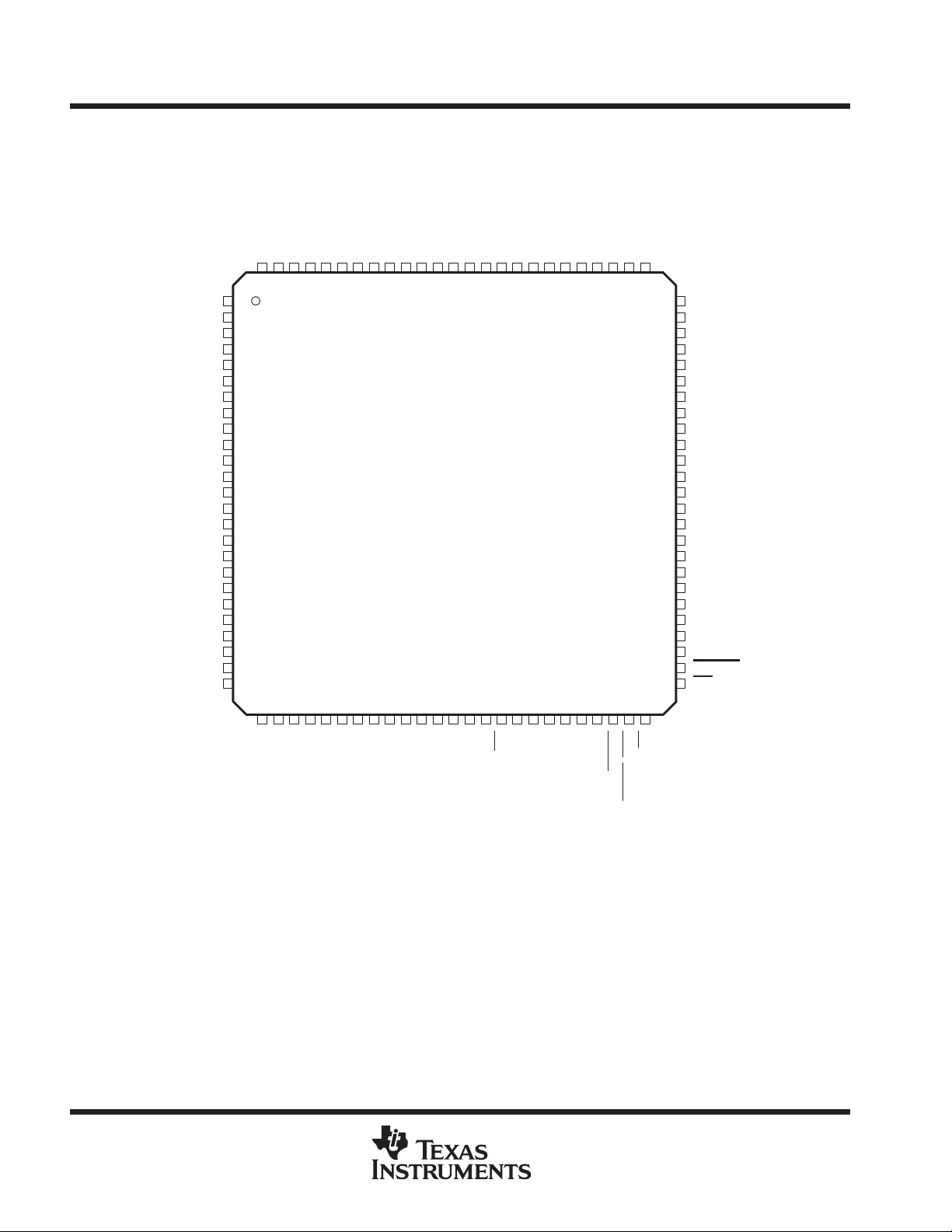
PZ PACKAGE
(TOP VIEW)
SS
NC
AVDD_FIL_RXVREFM
93
92
91
VMID_REF
89
90
TL V320AD11A
37
36
35
34
33
GP0
GP1
GP2
GP3
GP4
GP5
GP6
GP7
DVSS
NC
VMID_ADC
A VDD_ADC
A VSS_ADC
NC
DVDD_RX
DVSS_RX
D0
D1
D2
D3
D4
D5
D6
D7
D8
1
2
3
4
5
6
7
8
9
10
11
12
13
14
15
16
17
18
19
20
21
22
23
24
25
CONFIG2
OE_SYNC
ONE_WE
NC
97
98
99
100
29
28
27
26
RXM
RXP
AVSS_FIL_RX
94
95
96
32
31
30
REFPNCAVSS_FIL_TX
A VSS_REF
A VDD_REF
86
87
88
40
38
39
AVDD_FIL_TX
83
84
85
43
42
41
TXM
TXPNCECM
80
81
82
46
45
44
ECPNCNC
78
79
48
47
77
49
76
75
74
73
72
71
70
69
68
67
66
65
64
63
62
61
60
59
58
57
56
55
54
53
52
51
50
NC
NC
A VDD_FIL_EC
A VSS_FIL_EC
A VSS2_TX
A VDD2_TX
COMPB_TX
COMPA_TX
A VSS1_TX
A VDD1_TX
A VSS2_EC
A VDD2_EC
COMPA_EC
COMPB_EC
A VSS1_EC
A VDD1_EC
VCXOCNTL
DVSS
DVDD_DAC
DVSS_DAC
ADR1
ADR0
PWDN
RESET
CS
D9
D11
D10
DVSS_BF
DVDD_BF
NC – No connection (leave open)
2
D14
D12
D13
D15
SDO
POST OFFICE BOX 655303 • DALLAS, TEXAS 75265
FS
SDI
OSEN
SCLK/READY
INT
CLKIN
DVSS_CLK
CLKOUT/INT
SYNC
DVSS_LG
DVDD_CLK
DVDD_LG
OE
WETX
WEEC/CS2
Page 3
3.3 V INTEGRATED ADSL OVER POTS CODEC
I/O
DESCRIPTION
SLWS087B – JUNE 1999 – REVISED MARCH 2000
Terminal Functions
TERMINAL
NAME NO.
ADR0
ADR1
AVDD1_EC 60 I EC channel analog power supply #1
AVDD2_EC 64 I EC channel analog power supply #2
AVDD1_TX 66 I TX channel analog power supply #1
AVDD2_TX 70 I TX channel analog power supply #2
AVDD_ADC 12 I Receive channel analog power supply
AVDD_FIL_EC 73 I EC channel filter analog power supply
AVDD_FIL_RX 93 I Receive channel filter analog power supply
AVDD_FIL_TX 83 I Transmit channel filter analog power supply
AVDD_REF 86 I Reference analog power supply
AVSS1_EC 61 I EC channel analog ground # 1
AVSS2_EC 65 I EC channel analog ground #2
AVSS1_TX 67 I TX channel analog ground #1
AVSS2_TX 71 I TX channel analog ground #2
AVSS_ADC 13 I Receive channel analog ground
AVSS_FIL_EC 72 I EC channel filter analog ground
AVSS_FIL_RX 94 I Receive channel filter analog ground
AVSS_FIL_TX 84 I Transmit channel filter analog ground
AVSS_REF 87 I Reference analog ground
CLKIN 42 I 35.328 MHz VCXO clock input
CLKOUT/INT 41 O
COMPA_EC 63 O EC channel cap input A. Add 500 pF X7R ceramic capacitor to AVDD1_EC.
COMPB_EC 62 O EC channel cap input B. Add 1 µF X7R ceramic capacitor to AVDD1_EC.
COMPA_TX 68 O TX channel decoupling cap input A. Add 500 pF ceramic capacitor to AVDD1_TX.
COMPB_TX 69 O TX channel decoupling cap input B. Add 1 µF ceramic capacitor to AVDD1_TX.
CONFIG2 100 I
CS 51 I Parallel port chip select
D15
D14
D13
D12
D11
D10
D9
D8
D7
D6
D5
D4
D3
D2
D1
D0
54
55
34 (MSB)
33
32
31
30
29
28
25
24
23
22
21
20
19
18
17 (LSB)
I Serial port chip ID address bits, ADR0 is the least significant bit.
If CONFIG2 (pin 100) is low, this pin is 4.416 MHz clock output. If CONFIG2 is high, this pin functions as
.
INT
I/O configuration input pin. A high on this pin redefines the function of pins 37 and 41. The default state of
this pin is low. Refer to Figure 3 for details.
I/O Parallel port data bits D0=LSB
TLV320AD11A
POST OFFICE BOX 655303 • DALLAS, TEXAS 75265
3
Page 4
TLV320AD11A
3.3 V INTEGRATED ADSL OVER POTS CODEC
SLWS087B – JUNE 1999 – REVISED MARCH 2000
Terminal Functions(Continued)
TERMINAL
NAME NO.
DVDD_BF 26 I Digital I/O buffer supply
DVDD_CLK 44 I Digital clock supply
DVDD_LG 47 I Digital logic supply
DVDD_RX 15 I Receive channel digital power supply
DVDD_DAC 57 I Digital power supply for DAC
DVSS 9, 58 I Digital ground
DVSS_BF 27 I Digital I/O buffer ground
DVSS_CLK 43 I Digital clock ground
DVSS_LG 46 I Digital logic ground
DVSS_RX 16 I Receive channel ground
DVSS_DAC 56 I DAC ground
ECM 79 O EC output minus
ECP 78 O EC output plus
FS 38 I Frame sync input
GP7
GP6
GP5
GP4
GP3
GP2
GP1
GP0
INT 40 O Data rate clock (INT is 4.4 MHz when OSEN=1, 2.2 MHz when OSEN=0)
NC 10, 14, 74,
OE 50 I Parallel port output enable from host processor
OE_SYNC 99 I OE synchronized input. A high input will optimize the read operation from keep-out zone. The default
ONE_WE 98 I TX and EC write combined input. A high on this pin allows pin 48, WETX, to be used to write to both the
OSEN 39 I Over-sampling enable input. OSEN=1 enables over-sampling mode (INT = 4.4 MHz).
PWDN 53 I Power-down input. When PWDN=0, device is in normal operating mode. When PWDN=1, device is in
REFM 89 O Decoupling reference REF voltage minus. Add 10 µF tantalum and 0.1 µF ceramic capacitors to
REFP 88 O Decoupling reference REF voltage plus. Add 10 µF tantalum and 0.1 µF ceramic capacitors to
RESET 52 I H/W system reset. An low level will reset the device.
RXM 96 I Receive RX input minus. RXM is self-biased to AVDD_FIL_RX/2.
RXP 95 I Receive RX input plus. RXP is self-biased to AVDD_FIL_RX/2.
SCLK/READY 37 O If CONFIG2 (pin 100) is low, this pin is serial clock output. If CONFIG2 is high, it indicates the period in
SDI 36 I Serial data input
8
7
6
5
4
3
2
1
75, 76, 77,
80, 85, 91,
97
I/O DESCRIPTION
O General-purpose output port
No connection. All the NC pins should be left open.
state of this pin is low. See Figure 5 for details.
EC and TX channels. In this case, after a hardware reset or write to SCR14[0], the first low-going pulse of
will be a write to TX channel and the second one will be a write to EC channel. The default state of
WETX
this pin is low.
power-down mode.
AVSS_REFP. The nominal dc voltage at this terminal is 0.5 V . See figure 9 for detail.
AVSS_REFM. The nominal dc voltage at this terminal is 2.5 V.. See figure 9 for detail.
which parallel data can be transferred.
4
POST OFFICE BOX 655303 • DALLAS, TEXAS 75265
Page 5
TLV320AD11A
I/O
DESCRIPTION
3.3 V INTEGRATED ADSL OVER POTS CODEC
SLWS087B – JUNE 1999 – REVISED MARCH 2000
Terminal Functions(Continued)
TERMINAL
NAME NO.
SDO 35 O Serial data output
SYNC 45 I SYNC pulse for clock synchronization. A high pulse to the pin synchronizes the clock operation. The
TXM 82 O Transmit output minus
TXP 81 O Transmit output plus
VCXOCNTL 59 O VCXO DAC output
VMID_ADC 11 O Decoupling 1.5 V for ADC. Add 10 µF tantalum and 0.1 µF ceramic capacitors to AVSS_ADC.
VMID_REF 90 O Decoupling 1.5 V reference voltage. Add 10 µF tantalum and 0.1 µF ceramic capacitors to A VSS_REF.
V
SS
92 I Substrate. VSS needs to connect to analog ground.
WEEC/CS2 49 I Write enable to EC channel from host processor, when ONE_WE (pin 98) is low . If ONE_WE is high, it
WETX 48 I Write enable for TX channel from host processor. If ONE_WE is high, it functions as write enable for both
default state of the pin is low. Refer to Figure 4 for detail.
functions as second chip select, CS2
, and both CS and CS2 need to be low in order to have WETX
access data on the parallel bus.
TX and EC after hardware reset or write to SCR14[0]. In this case, the first low-going pulse of WETX
be a write to TX channel, and the second one will be a write to EC channel
will
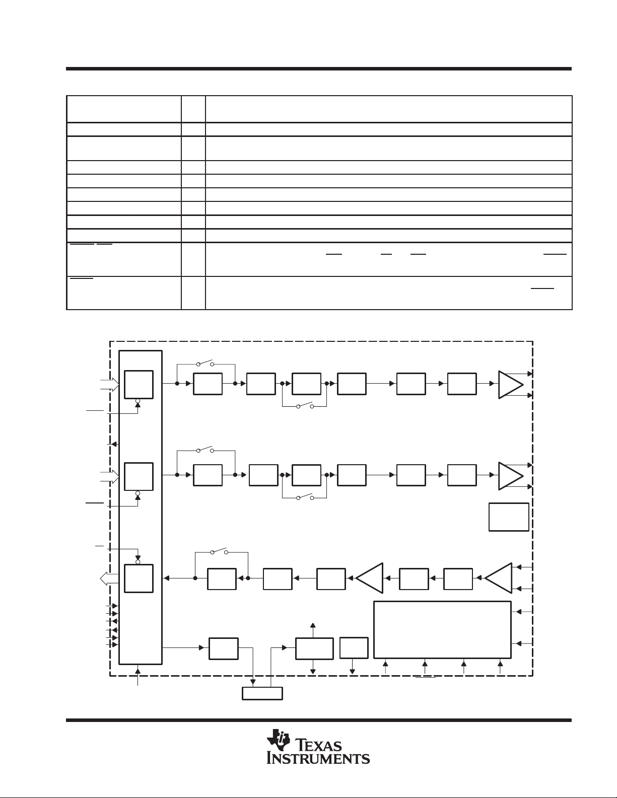
functional block diagram
D0–D15
WETX
D0–D15
WEEC
D0–D15
SCLK
ADR1
ADR0
INT
OE
SDI
SDO
FS
Input
Buffer
Parallel
Bus
Input
Buffer
CODEC
Interface
Output
Buffer
Serial
Interface
276 KSPS
276 KSPS
2208
KSPS
OSEN
INTRP
2×
OSEN
INTRP
2×
OSEN
DEC/2
VCXO
DAC
552
KSPS
552
KSPS
138 kHz
4416
KSPS
Digital
LPF
138 kHz
Digital
LPF
1.104 MHz
Digital
LPF
25.875 kHz
Digital
HPF
SCR7[0]
25.875 kHz
Digital
HPF
SCR14[2]
4416
KSPS
Clock
Generator
14 Bit
4.416 MSPS
RX
ADC
INTRP
8×
INTRP
8×
(0.25 dB/step)
4V
PP
GP0–7
4416
KSPS
4416
KSPS
0 to 11.5 dB
PGA2
4.416 MSPS
4.416 MSPS
1.104 MHz
3V
PP
14 Bit
TX
DAC
14 Bit
EC
DAC
RX
LPF
138 kHz
LPF
138 kHz
LPF
(25 dB Boost
5 dB/step)
RX
EQ
Control Block
TX
EC
0 to –24 dB
(–1 dB/step)
TX PAA
PAA
0 to –24 dB
(–1 dB/step)
EC PAA
PAA
Internal
Reference
0 to 6 dB
(1 dB/step)
PGA1
TXP
TXM
ECP
ECM
RXP
RXM
OE_SYNC
ONE_WE
OSEN
VCXOCNTL CLKIN
VCXO
35.328 MHz
POST OFFICE BOX 655303 • DALLAS, TEXAS 75265
CLKOUT
4.416 MHz
GP0–GP7
SYNC
RESET
PWDN CONFIG2
5
Page 6
TLV320AD11A
3.3 V INTEGRATED ADSL OVER POTS CODEC
SLWS087B – JUNE 1999 – REVISED MARCH 2000
PRINCIPLES OF OPERATION
communication channels
transmitter channel/echo-cancellation channel
The transmitter channel is powered by a high performance DAC. This is a 4.416-MHz, 14-bit DAC that provides a
16X over-sampling to reduce DAC noise. The input buffer is sampled at either 276 KSPS (pin OSEN = low,
default), or 552 KSPS (pin OSEN = high). A low-pass filter limits its output to 138 kHz. A programmable
attenuator, with a range between 0 and –24 dB in –1-dB steps, drives the output into the external ADSL line
driver.
A second transmitter is used to perform pre-echo cancellation. This analog echo cancellation helps reduce the
dynamic range requirements of the RT receiver . It has the same function as the first transmitter channel. It drives
a separate external line driver to perform the cancellation.
receiver channel
The receiver channel has two PGAs and an equalizer to match the loop loss and flatten the spectrum. This
results in a reduction in dynamic range requirement for the high resolution ADC. The receiver channel also has a
1.104-MHz low-pass filter with a 4.416 MSPS and a 14-bit ADC to provide a 2X over-sampling. The output buffer
is updated at either 2208 KSPS (pin OSEN = low, default), or 4416 KSPS (pin OSEN = high).
VCXO-control DAC
A 12-bit DAC is used to control the external 35.328-MHz VCXO (voltage control oscillator) that provides the
system clock to the codec. In a typical application, the typical update rate of the DAC is about 4 kHz, depending
on the ADSL frame rate. The host DSP initiates the update through the serial interface. The two 8-bit registers
SCR4 and SCR5 (each 2s complement) are used to generate the 12-bit code for the DAC. This requires the
use of 16 bits to obtain a 12-bit number. So the lower 4 bits of the MSB register (SCR5[3:0]) are added (2s
complement) to the higher 4 bits of the LSB register (SCR4[7:4]). Refer to Figure 1 for code generation. The
updated code is sent to the DAC two SCLKs after the SCR4 register is received. Notice that if SCR5 does not
need to be updated, only one write cycle to SCR4 is needed to update the VCXO DAC. In this case, the lower
8 bits of the 12-bit word will be updated.
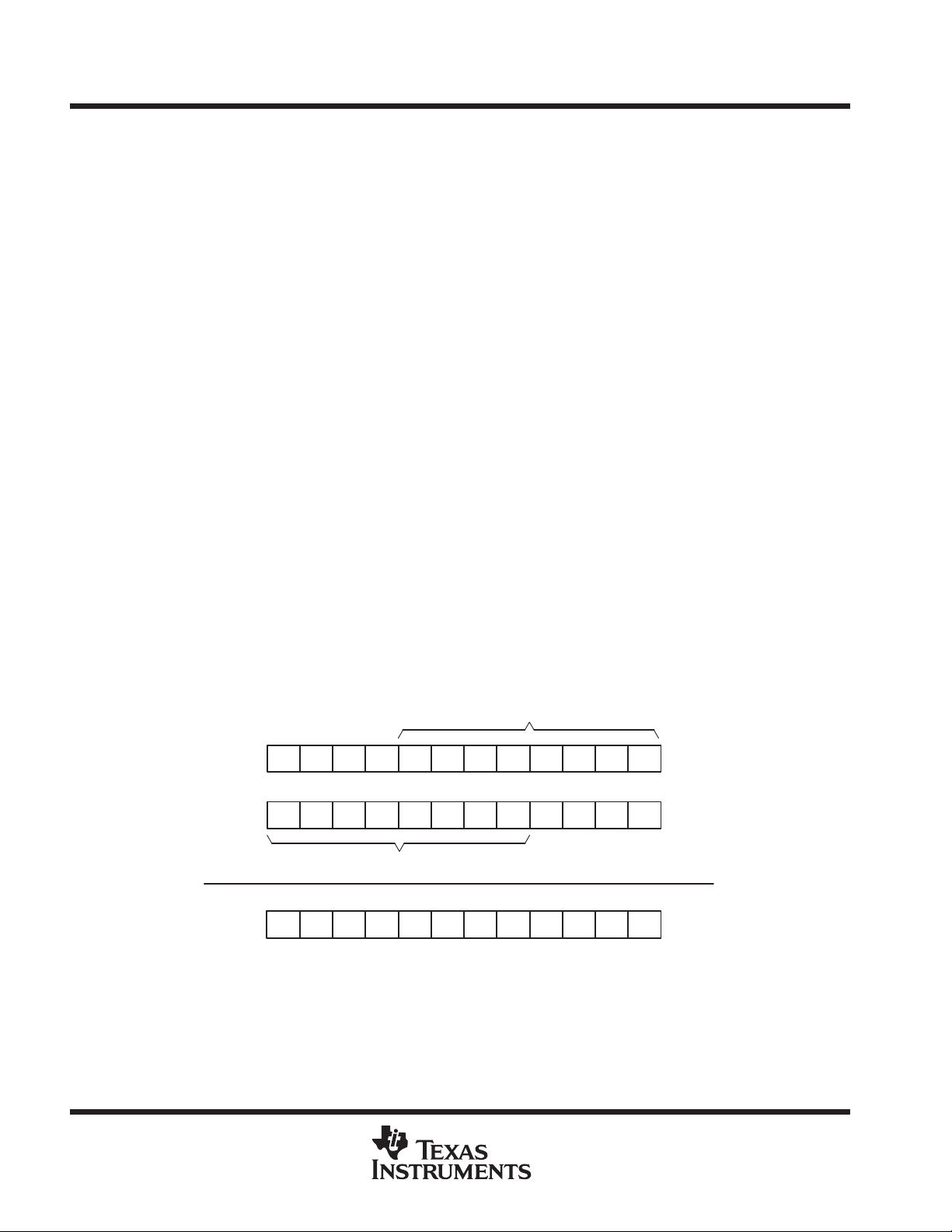
SCR4
D7
D7 D7 D7 D7 D6 D5 D4 D3 D2 D1 D0
D7 D6 D5 D4 D3 D2 D1 D0 0 0 0 0
+
D11 D10 D9 D8 D7 D6 D5 D4 D3 D2 D1 D0
SCR5
12-bit code for VCXO DAC
Figure 1. 12-Bit Code Generation for VCXO DAC
6
POST OFFICE BOX 655303 • DALLAS, TEXAS 75265
Page 7
TLV320AD11A
3.3 V INTEGRATED ADSL OVER POTS CODEC
SLWS087B – JUNE 1999 – REVISED MARCH 2000
PRINCIPLES OF OPERATION
communication channels (continued)
clock generation
The clock generation block provides the necessary clock signals for the device, with minimum skew and jitter.
This is closely dependent on the performance of the external VCXO. The external VCXO specifications are:
D
3.3 V supply
D
35.328 MHz ± 50 PPM
D
Minimum duty cycle is 60/40 (50/50 is optimum)
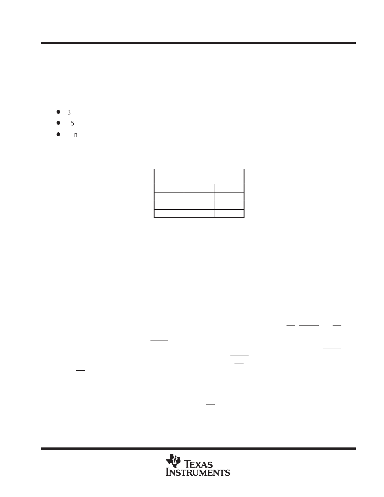
The major clocks generated internally are shown in Table 1.
Table 1. Clock Description
FREQUENCY
CLOCK
INT 2.208 4.416
CLKOUT 4.416 4.416
SCLK 4.416 4.416
(MHz)
OSEN=0 OSEN=1
INT
The interrupt (INT) to the host processor is 4.416 MHz when OSEN = 1 and 2.208 MHz when OSEN = 0.
SCLK
The serial clock used in the serial codec interface has a fixed frequency of 4.416 MHz and is synchronous with
the master clock (35.328 MHz).
CLKOUT
CLKOUT is a 4.416-MHz clock output, and is synchronous with the master clock (35.328 MHz).
interface
parallel interface
The device has a 16-bit parallel interface for transmitter and receiver data. Strobes OE, WETX, and CS from
the host DSP are edge-triggered signals. An incoming signal is registered on the rising edge of WETX/WEEC.
When ONE_WE is enabled, only WETX
channel write operation. After D0 of register SCR14 is programmed, the data from the first pulse of WETX goes
to the transmit channel, while the data from the second pulse of WETX goes to the echo-cancellation channel.
Output data from the codec is enabled after the falling edge of the OE strobe, and disabled after the rising edge
of the OE strobe. The INT cycle time is hardware-configurable to 4.416 MHz (2X over-sampling mode,
OSEN=1), or to 2.208 MHz (1X over-sampling mode, OSEN=0). SYNC is used to synchronize the operation
between the codec and the host transceiver. SCLK/READY is used to indicate the parallel data transfer period
in configuration mode 2. See Figure 3 for details.
is needed for both the transmit channel and the echo-cancellation
OE_SYNC is used to synchronize the codec timing to OE
. See Figure 5 for details.
For the 16-bit parallel data, D0 is the LSB and D15 is the MSB. The parallel TX and RX data contains 16 valid
bits. All 16 bits are used in the digital filtering.
POST OFFICE BOX 655303 • DALLAS, TEXAS 75265
7
Page 8

TLV320AD11A
3.3 V INTEGRATED ADSL OVER POTS CODEC
SLWS087B – JUNE 1999 – REVISED MARCH 2000
PRINCIPLES OF OPERATION
interface (continued)
keep-out zones
The last CLKIN cycle before a transition of CLKOUT is defined as a keep-out zone. These zones are reserved
for the sampling of analog signals. All digital I/O (except for CLKIN) should be quiet during these keep-out zones.
over-sampling mode
The OSEN pin selects 2X over-sampling mode (INT running at 4.416 MHz), or 1X over-sampling mode (INT
running at 2.208 MHz).
serial interface
The serial port is used for codec configuration and register reading. The word length is 16-bit. Two hardware
configuration terminals, ADR[1:0], are used to configure the device ID. Up to four codecs can be identified for
each common serial port. Refer to figure 6 for timing and format.
The master codec (ADR[1:0] = [0,0]) provides the SCLK to the host processor. The SCLK terminals on the other
codecs are left unconnected. All the codecs in a multi-codec system should be synchronized so that their SCLK
signals are in phase, even though the signals themselves are not being used. This ensures that, even though
the individual SCLK signals of each codec are not being used, the data is being latched into the codec properly .
The SCLK is a continuously running 4.416-MHz fixed-frequency clock, synchronized to the codec internal
events and CLKOUT (to the host) so that the keep-out zones may be monitored. A host DSP can drive the FS
(synchronized to the CLKOUT from the codec) into the codec to initiate a 16-bit serial I/O frame.
If SCR5 needs to be updated, the host controller (DSP) must first write the SCR5 of the VCXO DAC data, and
then the SCR4 of the VCXO DAC data. The VCXO DAC only gets updated after the SCR4 is written.
GP port
The general-purpose port provides eight outputs, each capable of delivering 0.5 mA, for control of external
circuitry such as LEDs, gain control, and power down.
voltage reference
The built-in reference provides the required reference voltage and current to individual analog blocks. It is also
brought out to external terminals for noise decoupling.
8
POST OFFICE BOX 655303 • DALLAS, TEXAS 75265
Page 9
TLV320AD11A
DEFAULT
SCR0
0000
3.3 V INTEGRATED ADSL OVER POTS CODEC
SLWS087B – JUNE 1999 – REVISED MARCH 2000
PRINCIPLES OF OPERATION
register programming (see Figure 6 for timing and format details)
Table 2. System Control Registers (SCR)
REGISTER
NAME
SCR1 0001 R/W 00000000
SCR2 0010 R/W 00000000 D[5:0]=RX PGA2. D[5:0]=000000 for 0 dB. D[5:0]=101110 for 11.5 dB.
SCR3 0011 R/W 00000000
SCR4 0100 R/W 00000000 D[7:0]=VCXODAC (low 8 bits of 12-bit DAC code)
SCR5 0101 R/W 00000000 D[7:0]=VCXODAC (high 8 bits of 12-bit DAC code)
SCR6 0110 R/W 00000000 D[7:0]=GP[7:0]
SCR7 0111 R/W 00000000
SCR8 1000 R/W 00000000
SCR9 1001 R/W 00000000 D[7:0]=RX offset low
SCR10 1010 R/W 00000000 D[7:0]=RX offset high
SCR11 1011 R/W 00000000
SCR12 1 100 R/W 00000000 D[2:0]=RX PGA1. D[2:0]=000 for 0 dB. D[2:0]=110 for 6 dB.
SCR13 1 101 R/W 00000000
SCR14 1110 R/W 00000000
NOTE 1: It is a two-stage FIFO buffer, and can store up to two write-samples if asynchronous write operation is required.
ADDRESS
S3, S2, S1, S0
MODE
R 00000000
W D0: S/W RESET (self clearing)
VALUE
D[4:0]=TX channel PAA gain select. D[4:0]=00000 for 0 dB
D[4:0]=1 1000 for –24 dB
D[2:0]= RX EQ slope select. D[2:0]=000 for 0dB/MHz, D[2:0]=001 for 5 dB/MHz,
D[2:0]=101 for 25 dB/MHz
MISC control (set to 1 to enable)
D0: bypass TX DHPF (25.875 kHz)
D1: S/W power-down RX channel
D2: S/W power-down TX channel
D3: analog loop-back (TX channel)
D4: digital loop-back (TX and EC channel)
D5: TX parallel interface (read-back) test mode enable
D6: EC channel power down
D7: EC analog loop-back
D[4:0]=EC channel PAA gain select. D[4:0]=00000 for 0 dB.
D[4:0]=1 1000 for –24 dB.
D[4:0]=TX digital gain select. The gain range is –1dB to 1dB in 0.1 dB-steps.
D[4:0]=00000 for 0 dB. D[4:0]=00001 for +0.1 dB. D[4:0]=01010 for +1 dB.
D[4:0]=10000 for –1 dB. D[4:0]=11001 for –0.1 dB.
D[4:0]=EC digital gain select. The gain range is –1dB to 1dB in 0.1-dB steps.
D[4:0]=00000 for 0 dB. D[4:0]=00001 for +0.1 dB. D[4:0]=01010 for +1 dB.
D[4:0]=10000 for –1 dB. D[4:0]=11001 for –0.1 dB.
D0: Sync the write operation when ONE_WE is selected. After D0 is set to 1, the first
pulse of WETX
The bit will be self-cleared to 0.
D1: enable FIFO (first-in, first-out). See Note 1.
D2: Bypass EC DHPF (25.875 kHz)
D3: ECNULL. When D3 is set to 1, ECP and ECM are connected to weakly driven
mid supply. It can only be used during EC power-down mode.
goes to TX channel, and the second pulse goes to EC channel.
FUNCTION
SCR0 – system control register Address:0000b Contents at reset: 00000000b
D7 D6 D5 D4 D3 D2 D1 D0
0 0 0 0 0 0 0 1 01 S/W reset (self clearing). All control registers are set to reset content.
REGISTER
VALUE (HEX)
POST OFFICE BOX 655303 • DALLAS, TEXAS 75265
DESCRIPTION
9
Page 10

TLV320AD11A
3.3 V INTEGRATED ADSL OVER POTS CODEC
SLWS087B – JUNE 1999 – REVISED MARCH 2000
PRINCIPLES OF OPERATION
register programming (continued)
SCR1 – TX PAA control register Address:0001b Contents at reset: 00000000b
D7 D6 D5 D4 D3 D2 D1 D0
0 0 0 0 0 0 0 0 00 TX PAA gain = 0 dB
0 0 0 0 0 0 0 1 01 TX PAA gain = –1 dB
0 0 0 0 0 0 1 0 02 TX PAA gain = –2 dB
0 0 0 0 0 0 1 1 03 TX PAA gain = –3 dB
0 0 0 0 0 1 0 0 04 TX PAA gain = –4 dB
0 0 0 0 0 1 0 1 05 TX PAA gain = –5 dB
0 0 0 0 0 1 1 0 06 TX PAA gain = –6 dB
0 0 0 0 0 1 1 1 07 TX PAA gain = –7 dB
0 0 0 0 1 0 0 0 08 TX PAA gain = –8 dB
0 0 0 0 1 0 0 1 09 TX PAA gain = –9 dB
0 0 0 0 1 0 1 0 0A TX PAA gain = –10 dB
0 0 0 0 1 0 1 1 0B TX PAA gain = –11 dB
0 0 0 0 1 1 0 0 0C TX PAA gain = –12 dB
0 0 0 0 1 1 0 1 0D TX PAA gain = –13 dB
0 0 0 0 1 1 1 0 0E TX PAA gain = –14 dB
0 0 0 0 1 1 1 1 0F TX PAA gain = –15 dB
0 0 0 1 0 0 0 0 10 TX PAA gain = –16 dB
0 0 0 1 0 0 0 1 11 TX PAA gain = –17 dB
0 0 0 1 0 0 1 0 12 TX PAA gain = –18 dB
0 0 0 1 0 0 1 1 13 TX PAA gain = –19 dB
0 0 0 1 0 1 0 0 14 TX PAA gain = –20 dB
0 0 0 1 0 1 0 1 15 TX PAA gain = –21 dB
0 0 0 1 0 1 1 0 16 TX PAA gain = –22 dB
0 0 0 1 0 1 1 1 17 TX PAA gain = –23 dB
0 0 0 1 1 0 0 0 18 TX PAA gain = –24 dB
– – – – – – – – 19–FF TX PAA gain = –24 dB
REGISTER
VALUE (HEX)
DESCRIPTION
10
POST OFFICE BOX 655303 • DALLAS, TEXAS 75265
Page 11

TLV320AD11A
3.3 V INTEGRATED ADSL OVER POTS CODEC
SLWS087B – JUNE 1999 – REVISED MARCH 2000
PRINCIPLES OF OPERATION
register programming (continued)
SCR2 – RX PGA2 control register Address:0010b Contents at reset: 00000000b
D7 D6 D5 D4 D3 D2 D1 D0
0 0 0 0 0 0 0 0 00 RX PGA2 = 0 dB
0 0 0 0 0 0 0 1 01 RX PGA2 = 0.25 dB
0 0 0 0 0 0 1 0 02 RX PGA2 = 0.5 dB
0 0 0 0 0 0 1 1 03 RX PGA2 = 0.75 dB
0 0 0 0 0 1 0 1 05 RX PGA2 = 1 dB
0 0 0 0 0 1 1 0 06 RX PGA2 = 1.25 dB
0 0 0 0 0 1 1 1 07 RX PGA2 = 1.5 dB
0 0 0 0 1 0 0 0 08 RX PGA2 = 1.75 dB
0 0 0 0 1 0 0 1 09 RX PGA2 = 2 dB
0 0 0 0 1 0 1 0 0A RX PGA2 = 2.25 dB
0 0 0 0 1 0 1 1 0B RX PGA2 = 2.5 dB
0 0 0 0 1 1 0 0 0C RX PGA2 = 2.75 dB
0 0 0 0 1 1 0 1 0D RX PGA2 = 3 dB
0 0 0 0 1 1 1 0 0E RX PGA2 = 3.25 dB
0 0 0 0 1 1 1 1 0F RX PGA2 = 3.5 dB
0 0 0 1 0 0 0 0 10 RX PGA2 = 3.75 dB
0 0 0 1 0 0 0 1 11 RX PGA2 = 4 dB
0 0 0 1 0 0 1 0 12 RX PGA2 = 4.25 dB
0 0 0 1 0 0 1 1 13 RX PGA2 = 4.5 dB
0 0 0 1 0 1 0 0 14 RX PGA2 = 4.75 dB
0 0 0 1 0 1 0 1 15 RX PGA2 = 5 dB
0 0 0 1 0 1 1 0 16 RX PGA2 = 5.25 dB
0 0 0 1 0 1 1 1 17 RX PGA2 = 5.5 dB
0 0 0 1 1 0 0 0 18 RX PGA2 = 5.75 dB
0 0 0 1 1 0 0 1 19 RX PGA2 = 6 dB
0 0 0 1 1 0 1 0 1A RX PGA2 = 6.25 dB
0 0 0 1 1 0 1 1 1B RX PGA2 = 6.5 dB
0 0 0 1 1 1 0 0 1C RX PGA2 = 6.75 dB
0 0 0 1 1 1 0 1 1D RX PGA2 = 7 dB
0 0 0 1 1 1 1 0 1E RX PGA2 = 7.25 dB
0 0 0 1 1 1 1 1 1F RX PGA2 = 7.5 dB
0 0 1 0 0 0 0 0 20 RX PGA2 = 7.75 dB
0 0 1 0 0 0 0 1 21 RX PGA2 = 8 dB
0 0 1 0 0 0 1 0 22 RX PGA2 = 8 25dB
0 0 1 0 0 0 1 1 23 RX PGA2 = 8.5 dB
0 0 1 0 0 1 0 0 24 RX PGA2 = 8.75 dB
0 0 1 0 0 1 0 1 25 RX PGA2 = 9 dB
0 0 0 0 0 1 0 0 04 RX PGA2 = 9.25 dB
0 0 1 0 0 1 1 0 26 RX PGA2 = 9.5 dB
0 0 1 0 0 1 1 1 27 RX PGA2 = 9.75 dB
0 0 1 0 1 0 0 0 28 RX PGA2 = 10 dB
0 0 1 0 1 0 0 1 29 RX PGA2 = 10.25 dB
REGISTER
VALUE (HEX)
DESCRIPTION
POST OFFICE BOX 655303 • DALLAS, TEXAS 75265
11
Page 12

TLV320AD11A
3.3 V INTEGRATED ADSL OVER POTS CODEC
SLWS087B – JUNE 1999 – REVISED MARCH 2000
PRINCIPLES OF OPERATION
register programming (continued)
SCR2 – RX PGA2 control register (continued) Address:0010b Contents at reset: 00000000b
D7 D6 D5 D4 D3 D2 D1 D0
0 0 1 0 1 0 1 0 2A RX PGA2 = 10.5 dB
0 0 1 0 1 0 1 1 2B RX PGA2 = 10.75 dB
0 0 1 0 1 1 0 0 2C RX PGA2 = 1 1 dB
0 0 1 0 1 1 0 1 2D RX PGA2 = 1 1.25 dB
0 0 1 0 1 1 1 0 2E RX PGA2 = 11.5 dB
– – – – – – – – 2F–FF RX PGA2 = 11.5 dB
SCR3 – RX EQ control register Address:0011b Contents at reset: 00000000b
REGISTER
VALUE (HEX)
DESCRIPTION
D7 D6 D5 D4 D3 D2 D1 D0
0 0 0 0 0 0 0 0 00 RX EQ = 0 dB/MHz
0 0 0 0 0 0 0 1 01 RX EQ = 5 dB/MHz
0 0 0 0 0 0 1 0 02 RX EQ = 10 dB/MHz
0 0 0 0 0 0 1 1 03 RX EQ = 15 dB/MHz
0 0 0 0 0 1 0 0 04 RX EQ = 20 dB/MHz
0 0 0 0 0 1 0 1 05 RX EQ = 25 dB/MHz
– – – – – – – – 06–FF RX EQ = 25 dB/MHz
REGISTER
VALUE (HEX)
DESCRIPTION
SCR4 – VCXO data register Address:0100b Contents at reset: 00000000b
SCR5 – VCXO data register Address:0101b Contents at reset: 00000000b
The following table shows some representative analog outputs. Notice that the read-back values of SCR4 and
SCR5 are different from the values written in.
Table 3. VCXODAC Digital-Analog Mapping
OPERATION HEX RESULT
SRC5[7:0] × 24 + SCR4[7:0]
NOTES: 2. ∆ = (3/4095) V
3. The analog output is computed as follows:
((SCR%[7:0] × 24 + SCR4[7:0])) + 2048(decimal) × ∆
0x800 0 V Min scale
0x801 ∆V Just above min
... ... ...
0xFFF 2047 ∆V Just below mid
0x000 2048 ∆V Mid scale
0x001 2049 ∆V Just above mid
... ... ...
0x7FE 4094 ∆V Just below max
0x7FF 4095 ∆V Max scale
ANALOG OUTPUT
(see Note 2 and 3)
COMMENTS
12
POST OFFICE BOX 655303 • DALLAS, TEXAS 75265
Page 13

register programming (continued)
examples:
• Positive SCR5 + positive SCR4
(0x24 × 24 + 0x42) = 0×240 + 0×42 = 0×282 = 642 decimal
Analog output = (642 + 2048) ∆V = 2690 ∆V = 1.971 V
The read back values of SCR5 and SCR4 are 0×02 and 0×82
TLV320AD11A
3.3 V INTEGRATED ADSL OVER POTS CODEC
SLWS087B – JUNE 1999 – REVISED MARCH 2000
PRINCIPLES OF OPERATION
• Positive SCR5 + negative SCR4
(0x24 × 2
Analog output = (514 + 2048) ∆V = 2562 ∆V = 1.877 V
The read back values of SCR5 and SCR4 are 0×02 and 0×02
4
+ 0×C2) = 0×240 + 0×FC2 = 0×202 = 514 decimal
• Negative SCR5 + positive SCR4
(0xA2 × 24 + 0×42) = 0×A20 + 0×42 = 0×A62 = –1438 decimal
Analog output = (–1438 + 2048) ∆V = 610 ∆V = 0.447 V
The read back values of SCR5 and SCR4 are 0×0A and 0×62
• Negative SCR5 + negative SCR4
(0xA2 × 24 + 0×C2) = 0×A20 + 0×FC2 = 0×9E2 = –1566 decimal
Analog output = (–1566 + 2048) ∆V = 482 ∆V = 0.353 V
The read back values of SCR5 and SCR4 are 0×09 and 0×E2
SCR6 – general-purpose output data register Address:0110b Contents at reset: 00000000b
D7 D6 D5 D4 D3 D2 D1 D0
0/1 – – – – – – – GP7 = low(0)/high(1)
– 0/1 – – – – – – GP6 = low(0)/high(1)
– – 0/1 – – – – – GP5 = low(0)/high(1)
– – – 0/1 – – – – GP4 = low(0)/high(1)
– – – – 0/1 – – – GP3 = low(0)/high(1)
– – – – – 0/1 – – GP2 = low(0)/high(1)
– – – – – – 0/1 – GP1 = low(0)/high(1)
– – – – – – – 0/1 GP0 = low(0)/high(1)
REGISTER
VALUE (HEX)
DESCRIPTION
POST OFFICE BOX 655303 • DALLAS, TEXAS 75265
13
Page 14

TLV320AD11A
3.3 V INTEGRATED ADSL OVER POTS CODEC
SLWS087B – JUNE 1999 – REVISED MARCH 2000
PRINCIPLES OF OPERATION
register programming (continued)
SCR7 – miscellaneous control register 1 Address:0111b Contents at reset: 00000000b
D7 D6 D5 D4 D3 D2 D1 D0
– – – – – – – 1 Bypass TX DHPF (25.875 kHz)
– – – – – – 1 – S/W power-down RX channel
– – – – – 1 – – S/W power-down TX channel
– – – – 1 – – – Analog loop-back (TX channel) (see Note 4)
– – – 1 – – – – Digital loop-back (TX and EC channel) (see Note 5)
– – 1 – – – – – TX parallel interface (read back) test mode enable (see Note 6)
– 1 – – – – – – EC channel power down
1 – – – – – – – EC analog loop-back
NOTES: 4. Analog loop-back: Analog output pins (TXP/TXM or ECP/ECM) are internally connected to RXP/RXM.
5. Digital loop-back: RX digital output buffer (16-bit word) is internally connected to the TX/EC digital input buffer.
6. The input digital data is read back from RX output buffer without going through DAC converter.
REGISTER
VALUE (HEX)
DESCRIPTION
SCR8 – EC PAA control register Address: 1000b Contents at reset: 00000000b
SCR8 shares the same format with SCR1. Check with SCR1 for detail
SCR9 – RX offset control register[7:0] Address:1001b Contents at reset: 00000000b
SCR10 – RX offset control register [15:8] Address:1010b Contents at reset: 00000000b
These two registers are concatenated to form a 16-bit word in 2s complement data format. The 16-bit word is
used to adjust RX channel dc offset error. It adds to the 16-bit data from the RX digital filter before the data goes
to the RX output buffer.
14
POST OFFICE BOX 655303 • DALLAS, TEXAS 75265
Page 15

TLV320AD11A
3.3 V INTEGRATED ADSL OVER POTS CODEC
SLWS087B – JUNE 1999 – REVISED MARCH 2000
PRINCIPLES OF OPERATION
register programming (continued)
SCR11 – TX channel digital gain control register Address: 1011b Contents at reset: 00000000b
(see Note 7)
D7 D6 D5 D4 D3 D2 D1 D0
0 0 0 1 1 0 0 1 19 TX digital gain = –0.1 dB
0 0 0 1 1 0 0 0 18 TX digital gain = –0.2 dB
0 0 0 1 0 1 1 1 17 TX digital gain = –0.3 dB
0 0 0 1 0 1 1 0 16 TX digital gain = –0.4 dB
0 0 0 1 0 1 0 1 15 TX digital gain = –0.5 dB
0 0 0 1 0 1 0 0 14 TX digital gain = –0.6 dB
0 0 0 1 0 0 1 1 13 TX digital gain = –0.7 dB
0 0 0 1 0 0 1 0 12 TX digital gain = –0.8 dB
0 0 0 1 0 0 0 1 11 TX digital gain = –0.9 dB
0 0 0 1 0 0 0 0 10 TX digital gain = –1 dB
0 0 0 0 0 0 0 0 00 TX digital gain = 0 dB
0 0 0 0 0 0 0 1 01 TX digital gain = 0.1 dB
0 0 0 0 0 0 1 0 02 TX digital gain = 0.2 dB
0 0 0 0 0 0 1 1 03 TX digital gain = 0.3 dB
0 0 0 0 0 1 0 0 04 TX digital gain = 0.4 dB
0 0 0 0 0 1 0 1 05 TX digital gain = 0.5 dB
0 0 0 0 0 1 1 0 06 TX digital gain = 0.6 dB
0 0 0 0 0 1 1 1 07 TX digital gain = 0.7 dB
0 0 0 0 1 0 0 0 08 TX digital gain = 0.8 dB
0 0 0 0 1 0 0 1 09 TX digital gain = 0.9 dB
0 0 0 0 1 0 1 0 0A TX digital gain = 1 dB
– – – – – – – – All others Reserved (see Note 8)
NOTES: 7. Digital gain is used to compensate the TX channel gain error.
8. Performance of the codec for invalid combination of bits should not be used. The user should make no assumption that the code
bits will saturate to a maximum or minimum value or wrap around to a valid combination.
REGISTER
VALUE (HEX)
DESCRIPTION
SCR12 – RX PGA1 control register Address:1100b Contents at reset: 00000000b
D7 D6 D5 D4 D3 D2 D1 D0
0 0 0 0 0 0 0 0 00 RX PGA1 = 0 dB
0 0 0 0 0 0 0 1 01 RX PGA1 = 1 dB
0 0 0 0 0 0 1 0 02 RX PGA1 = 2 dB
0 0 0 0 0 0 1 1 03 RX PGA1 = 3 dB
0 0 0 0 0 1 0 0 04 RX PGA1 = 4 dB
0 0 0 0 0 1 0 1 05 RX PGA1 = 5 dB
0 0 0 0 0 1 1 0 06 RX PGA1 = 6 dB
– – – – – – – – 07–FF RX PGA1 = 6 dB
REGISTER
VALUE (HEX)
POST OFFICE BOX 655303 • DALLAS, TEXAS 75265
DESCRIPTION
15
Page 16

TLV320AD11A
3.3 V INTEGRATED ADSL OVER POTS CODEC
SLWS087B – JUNE 1999 – REVISED MARCH 2000
PRINCIPLES OF OPERATION
register programming (continued)
SCR13 – EC channel digital gain control register Address:1101b Contents at reset: 00000000b
SCR13 has the same format as SCR11. Check with SCR11 for details.
SCR14 – Miscellaneous control register 2 Address:1110b Contents at reset: 00000000b
D7 D6 D5 D4 D3 D2 D1 D0
0 0 0 0 – – – 1 One write operation reset. (see Note 9)
0 0 0 0 – – 1 – Enable FIFO
0 0 0 0 – 1 – – Bypass EC DHPF (25.875 kHz)
0 0 0 0 1 – – – ECP and ECM are connected to weakly driven mid-supply. It can only be
NOTE 9: Write-synchronized operation: A 1 is written to bit D0 of SCR14 register after pin ONE_WE is set to high. This sets the start point for
the TX/EC operation. During the first WETX pulse, data is written to the TX channel. During the second WETX pulse, data is written
to the EC channel. D0 of SCR14 is always self-cleared; therefore, the read-back value of bit D0 of SCR14 is always zero.
REGISTER
VALUE (HEX)
DESCRIPTION
used during EC power-down mode.
device initialization time
The TLV320AD11A completes all calibration and initialization in less than 1 second. This includes reference
settling time (≈950 µs), one rest after power up (1 serial frame), VCXODAC configuration (2 serial frames),
TX/RX gain select (4 serial frames), and self-calibration of the DAC (256X1 13 ns). Each 16-bit frame requires
up to 5 µs. The host processor needs to initiate this process upon a successful power up.
power-down
Both hardware and software power-down modes are provided. The serial interface is operative when the codec
is in power-down mode. By sending commands through serial interface, either the codec or part of the codec,
can be software powered down. All the references are kept on in the software power-down mode. The codec
can also be hardware powered down by setting PWDN pin to high. All the references are shut off in the hardware
power-down mode. The contents of the registers will not change in either power-down modes.
power supply grouping recommendation
The following power supply grouping is recommended for best performance of this device. Ferrite beads are
used to separate group1, group 2, and group 3 if the same 3.3-V analog power source is shared
D
Group 1: AVDD_FIL_TX, AVDD_FIL_EC, AVDD1_TX, AVDD2_TX, AVDD1_EC, A VDD2_EC
D
Group 2: AVDD_FIL_RX, AVDD_ADC
D
Group 3: AVDD_REF
D
Group 4: DVDD_BF, DVDD_CLK, DVDD_LG, DVDD_RX, DVDD_DAC
16
POST OFFICE BOX 655303 • DALLAS, TEXAS 75265
Page 17

TLV320AD11A
V
Analog input signal range
DVDD_CLK=3.3 V
3.3 V INTEGRATED ADSL OVER POTS CODEC
SLWS087B – JUNE 1999 – REVISED MARCH 2000
absolute maximum ratings over operating free-air temperature (unless otherwise noted)
†
Supply voltage, AVDD to AGND, DVDD to DGND –0.3 V to 4.5 V. . . . . . . . . . . . . . . . . . . . . . . . . . . . . . . . . . . . .
Analog input voltage range to AGND –0.3 V to AVDD+0.3 V. . . . . . . . . . . . . . . . . . . . . . . . . . . . . . . . . . . . . . . . .
Digital input voltage range to DGND –0.3 V to DVDD+0.3 V. . . . . . . . . . . . . . . . . . . . . . . . . . . . . . . . . . . . . . . . . .
Operating
virtual junction temperature range, T
Operating free-air temperature range, T
Storage temperature range, T
–65°C to 150°C. . . . . . . . . . . . . . . . . . . . . . . . . . . . . . . . . . . . . . . . . . . . . . . . . . .
str
A
–40°C to 150°C. . . . . . . . . . . . . . . . . . . . . . . . . . . . . . . . . . . . .
J
–40°C to 85°C. . . . . . . . . . . . . . . . . . . . . . . . . . . . . . . . . . . . . . . . . . . .
Lead temperature 1,6 mm (1/16 inch) from case for 10 seconds 260°C. . . . . . . . . . . . . . . . . . . . . . . . . . . . . . .
†
Stresses beyond those listed under “absolute maximum ratings” may cause permanent damage to the device. These are stress ratings only, and
functional operation of the device at these or any other conditions beyond those indicated under “recommended operating conditions” is not
implied. Exposure to absolute-maximum-rated conditions for extended periods may affect device reliability.
recommended operating conditions
power supply
MIN NOM MAX UNIT
AVDD_FIL_TX, AVDD_FIL_EC, AVDD1_TX, AVDD2_TX, AVDD1_EC, AVDD2_EC;
Supply voltage
AVDD_FIL_RX, AVDD_ADC;
AVDD_REF
DVDD_BF, DVDD_CLK, DVDD_LG, DVDD_RX, DVDD_DAC 3 3.3 3.6
digital inputs
High-level input voltage, V
Low-level input voltage, V
II = 0.75 mA 2
IH
II = –0.75 mA 0.8
IL
3 3.3 3.6
MIN NOM MAX UNIT
V
analog input
p
clock inputs
Input clock frequency
Input clock duty cycle
MIN NOM MAX UNIT
AVDD_FIL_RX = 3.3 V. The input signal is measured single-ended. AVDD_FIL_RX/2±0.75 V
AVDD_FIL_RX = 3.3 V. The input signal is measured differentially. 3 Vp–p
MIN NOM MAX UNIT
35.328 MHz
50%
POST OFFICE BOX 655303 • DALLAS, TEXAS 75265
17
Page 18

TLV320AD11A
Conversion rate
MH
Full scale output voltage
g
dB
AVDD_REF
V
V
V
3.3 V INTEGRATED ADSL OVER POTS CODEC
SLWS087B – JUNE 1999 – REVISED MARCH 2000
electrical characteristics over recommended operating free-air temperature range, typical at TA =
25°C, f
CLKIN
otherwise noted)
TX and EC channel (measured differentially unless otherwise noted)
Signal bandwidth 138 kHz
Channel gain error PAA = 0 dB, Input = 99.1875 kHz at 06 dB –0.1 0.1 dB
PAA step gain error –0.2 0.2 dB
DC offset –70 70 mV
Cross–talk RX to TX channel (43.125 kHz at –1 dB) –65 dB
Group delay 6 µs
Power supply reject ratio (PSRR) 200 mVpp at 99.1875 kHz 50 dB
AC Performance
SNR Signal-to-noise ratio 81 dB
THD T otal harmonic distortion ratio
TSNR Signal-to-noise + harmonic distortion ratio 80 dB
MT Missing-tone test (see Note 11) 120.750 kHz (missing-tone) 76 dB
Channel Frequency Response (refer to Figure 7)
Gain relative to gain at 99.1875
(25.875 kHz DHPF is bypassed)
NOTES: 10. The input signal is the digital equivalent of a sine wave (digital full scale = 0 dB). The nominal differential output with this input
11. 27 tones, 25.875 to 138 kHz, 4.3125 kHz/step, –1 dB
= 35.328 MHz, analog power supply = 3.3 V, digital power supply = 3.3 V (unless
PARAMETER TEST CONDITIONS MIN TYP MAX UNIT
OSEN pin high 4.416
OSEN pin low 2.208
p
condition is 3 Vpp.
Load = 2000 Ω, single-ended measured AVDD_TX/2±0.75 V
Load = 4000 Ω, differentially measured 3 Vp–p
43.125 kHz at –1 dB (see Note 10)
30 kHz –0.25 0.25
60 kHz
138 kHz
276 kHz –55
–0.25 0.25
86 dB
–3
z
reference outputs (see Note 12)
REFP REF plus input voltage 2.5
REFM REF minus input voltage
VMID_REF REF mid input voltage
VMID_ADC Receive channel mid-input voltage 1.5
NOTE 12: All the reference outputs should not be used as voltage source.
digital outputs
V
OH
V
OL
18
PARAMETER TEST CONDITIONS MIN TYP MAX UNIT
= 3.3
PARAMETER TEST CONDITIONS MIN TYP MAX UNIT
High-level output voltage IOH = 0.5 mA 2.4
Low-level output voltage IOL = –0.5 mA 0.6
POST OFFICE BOX 655303 • DALLAS, TEXAS 75265
0.5
1.5
Page 19

TLV320AD11A
PGA gain error
dB
MT
Missing-tone test (see Note 14)
dB
g
dB
Power-down mode
3.3 V INTEGRATED ADSL OVER POTS CODEC
SLWS087B – JUNE 1999 – REVISED MARCH 2000
electrical characteristics over recommended operating free-air temperature range (unless
otherwise noted), typical at T
= 25°C, f
A
CLKIN
power supply = 3.3 V (unless otherwise noted) (continued)
RX channel (measured differentially unless otherwise noted)
PARAMETER TEST CONDITIONS MIN TYP MAX UNIT
Signal bandwidth 1104 kHz
Conversion rate 4.416 MHz
Channel gain error
DC offset PGA1 = 0 dB, PGA2 = 2.5 dB 3 mV
Crosstalk
Group delay 8 µs
Common mode reject ratio (CMRR) 99.1875 kHz at –1 dB 70 dB
Power supply reject ratio (PSRR) 200 mVpp at 99.1875 kHz 50 dB
Analog input self-bias dc voltage AVDD_FIL_RX/2 ±0.75 V
Input impedance 10 kΩ
AC Performance
SNR Signal-to-noise ratio 68
THD T otal harmonic distortion ratio
TSNR Signal-to-noise + harmonic distortion ratio 68
Channel Frequency Response (EQ[2:0] = 0 dB/MHz) (refer to Figure 8)
Gain relative to gain at 99.1875 kHz
NOTES: 13. The analog input test signal is a sine wave with 0 dB = 3 Vpp as the reference level.
VCXO DAC
14. 250 tones, 25.875 to 1104 kHz, 4.3125 kHz/step, 0 dB.
PARAMETER TEST CONDITIONS MIN TYP MAX UNIT
Resolution 12 Bits
DNL Differential nonlinearity ±1 LSB
INL Integral nonlinearity ±4 LSB
Offset error 30 mV
Analog output Full scale output voltage Load = 50 kΩ and VDD = 3.3 V 3 V
= 35.328 MHz, analog power supply = 3.3 V, digital
PGA1 = 0 dB, PGA2 = 2.5 dB,
Input = 99.1875 kHz at –1 dB
PGA1 (0 to 6 dB at 1 dB/step) –0.2 0.2
PGA2 (2.5 to 14 dB at 0.25 dB/step) –0.03 0.03
TX to RX channel (99.1875 kHz at –1 dB
see Note 13)
99.1875 kHz at 0 dB
120.750 kHz (missing-tone) 66
750.375 kHz (missing-tone) 66
60 kHz –0.25 0.25
300 kHz
800 kHz 1
1000 kHz 0.7
–1.5 1.5 dB
63 dB
77
–0.25 0.25
dB
power dissipation
Power dissipation
PARAMETER TEST CONDITIONS MIN TYP MAX UNIT
Active mode 800 850
Hardware power down 65
Software power down 70
POST OFFICE BOX 655303 • DALLAS, TEXAS 75265
mW
19
Page 20

TLV320AD11A
tc2Cycle time, INT
3.3 V INTEGRATED ADSL OVER POTS CODEC
SLWS087B – JUNE 1999 – REVISED MARCH 2000
timing requirements over recommended ranges of supply voltage and operating free-air
temperature (unless otherwise noted)
parallel port (see Figures 2, 3, and 4)
PARAMETER MIN TYP MAX UNIT
t
Period, CLKIN 28.3 ns
c1
OSEN=0 16
OSEN=1 8
t
Period, CLKOUT 8
c3
t
Delay time, keep-out zone end to INT↑ 5 ns
d1
t
Delay time, keep-out zone end (CLKIN↑)to OE↓/CS↓ 0 ns
d2
t
Delay time, keep-out zone end to WETX↓/CS↓ or WEEC↓/CS↓ 0 ns
d3
t
Delay time, data valid after OE↓/CS↓ 15 ns
d4
t
Delay time, data becomes Hi-Z after OE↑/CS↑ 5 ns
d5
t
Delay time, keep-out zone end to SCLK/READY↑ 14.2 ns
d6
t
Delay time, SCLK/READY↓ to keep-out zone 14.2 ns
d7
t
Delay time, time between the rising edge of WETX/WEEC to the rising edge of CS 5 ns
d9
t
Hold time, data valid after WETX↑ 5 ns
h1
t
Hold time, data valid after WEEC↑ 5 ns
h2
t
Hold time, SYNC keep high after CLKIN↑ 5 ns
h3
t
Setup time, data valid before WETX↑ 15 ns
su1
t
Setup time, data valid before WEEC↑ or second WETX↑ 15 ns
su2
t
Setup time, SYNC is high before CLKIN↑ 10 ns
su3
t
Pulse width, keep-out zone time 1 CLKIN
w1
t
Pulse width, OE 20 ns
w2
t
Pulse width, WETX or WETX first pulse 28 ns
w3
t
Pulse width, WEEC or WETX second pulse 28 ns
w4
t
Pulse width, SYNC 28 ns
w5
CLKIN
serial port (see Figure 6)
t
Cycle time, SCLK 8 CLKIN
c4
t
Delay time, SCLK rising edge to SDO valid 15 ns
d8
t
Hold time, FS keep high after SCLK↓ 5 ns
h4
t
SDI valid after SCLK↓ 5 ns
h5
t
Setup time, FS valid before SCLK↓ 20 ns
su4
t
SDI valid before SCLK↓ 20 ns
su5
t
FS pulse width 28 ns
w6
PARAMETER MIN TYP MAX UNIT
20
POST OFFICE BOX 655303 • DALLAS, TEXAS 75265
Page 21

CONFIG2=0 or floating
CLKIN
(35.328 MHz)
(Input)
INT
(OSEN = 0)
(Output)
INT
(OSEN = 1)
(Output)
CLKOUT
(Output)
CS
(Input)
(see Note A)
OE
(RXADC)
(Input)
(see Note A)
WETX
(TXDAC)
(Input)
(see Note B)
WEEC
(TXDAC)
(Input)
(see Note B)
D0–D15
(Input/Output)
t
c1
t
d1
t
w2
t
d5
3.3 V INTEGRATED ADSL OVER POTS CODEC
PARAMETER MEASUREMENT INFORMATION
Keep-Out Zones
t
w1
t
c2
t
c3
t
d2
t
d3
t
t
w3
t
su1
t
d4
t
h1
d9
t
c2
t
TLV320AD11A
SLWS087B – JUNE 1999 – REVISED MARCH 2000
t
d3
d9
t
w4
t
su2
t
h2
Access Zone Access Zone Access Zone Access Zone Access Zone
NOTES: A. CS AND OE may fall/rise together or be skewed from each other . It does not matter which falls/rises first. However , td4 is referenced
from whichever falls last, and td5 is referenced from whichever rises first. CS
and WETX/WEEC may fall together or be skewed from each other. But the rising edge of WETX and WEEC should occur prior
B. CS
can be connected to low if the parallel bus is not shared.
to the rising edge of CS.
C. The minimum update rate for TX and EC channel is 276 kHz in normal mode, and 552 kHz in over-sampling mode. The write
operation for Tx and EC can occur at any time, if they do not conflict with each other or the Rx read cycle.
Figure 2. Parallel Timing Diagram
POST OFFICE BOX 655303 • DALLAS, TEXAS 75265
21
Page 22

TLV320AD11A
3.3 V INTEGRATED ADSL OVER POTS CODEC
SLWS087B – JUNE 1999 – REVISED MARCH 2000
PARAMETER MEASUREMENT INFORMATION
CONFIG2=1 and ONE_WE selected
Keep-Out Zones
CLKIN
(35.328 MHz)
(Input)
INT
(OSEN = 0)
(Output)
INT
(OSEN = 1)
(Output)
CLKOUT
(Output)
CS
(Input)
(see Note A)
OE
(RXADC)
(Input)
(see Note A)
WETX
(TXDAC)
(Input)
(see Note B)
D0–D15
(Input/Output)
t
c1
t
d1
t
d2
t
w5
t
d5
t
d4
t
w1
t
c2
t
c3
t
d3
t
d9
t
w3
t
su1
t
h1
t
c2
t
d3
t
d9
t
w4
t
su2
t
h2
Access Zone Access Zone Access Zone Access Zone Access Zone
NOTES: A. CS AND OE may fall/rise together or be skewed from each other . It does not matter which falls/rises first. However , td4 is referenced
from whichever falls last, and td5 is referenced from whichever rises first. CS
B. CS
and WETX may fall together or be skewed from each other. But the rising edge of WETX and WEEC should occur prior to the
can be connected to low if the parallel bus is not shared.
rising edge of CS.
C. The minimum update rate for TX and EC channel is 276 kHz in normal mode, and 552 kHz in over-sampling mode. The write
operation for Tx and EC can occur at any time, if they do not conflict with each other or the Rx read cycle.
Figure 3. Parallel Timing Diagram
22
POST OFFICE BOX 655303 • DALLAS, TEXAS 75265
Page 23

CLKIN
(35.328 MHz)
(Input)
SYNC
(Input)
INT
(Output)
CLKOUT
(Output)
3.3 V INTEGRATED ADSL OVER POTS CODEC
PARAMETER MEASUREMENT INFORMATION
12345678
t
su3
t
h3
t
w5
TLV320AD11A
SLWS087B – JUNE 1999 – REVISED MARCH 2000
Keep-Out Zone
SCLK
(Output)
Rising edge of INT and CLKOUT occurs on eighth
rising of CLKIN after SYNC pulse is sampled high.
Figure 4. SYNC Pulse Timing
CLKIN
(35.328 MHz)
(Input)
OE
(Input)
Keep-Out Zone Keep-Out Zone Keep-Out Zone Keep-Out Zone
NOTES: A. It takes about 16 CLKINs to shift the keep-out-zone out of the OE pulse.
need to be periodic signal.
B. OE
Figure 5. OE_SYNC Pulse Timing (OE_SYNC is set to high)
POST OFFICE BOX 655303 • DALLAS, TEXAS 75265
23
Page 24

TLV320AD11A
3.3 V INTEGRATED ADSL OVER POTS CODEC
SLWS087B – JUNE 1999 – REVISED MARCH 2000
PARAMETER MEASUREMENT INFORMATION
t
w6
FS
(Input)
t
R/W
h4
ADR1ADR
S3 S2 S1 S0 X D7 D6 D2 D1 D0
0
SCLK
(Output)
SDI
(Input)
t
su4
t
su5
t
c4
t
h5
D5 D4 D3
SDO
(Output)
(Read: R/W = 1)
SDO
(Output)
(Write: R/W = 0)
NOTES: A. Data on SDI is latched at the falling edge of SCLK.
B. Data is sent to SDO at the rising edge of SCLK.
C. ADR0 and ADR1 are the hardware configurable of ADR0 and ADR1 input pins.
See Note C
Hi-Z
Hi-Z
Figure 6. Serial Port Timing
6
1 × 10
–50
–100
–150
2 × 10
D7 D6 D2 D1 D0D5 D4 D3
t
d8
6
3 × 10
6
4 × 10
6
Hi-Z
24
–200
–250
Figure 7. TX/EC Channel Filter Response (25.875 kHz DHPF is bypassed)
POST OFFICE BOX 655303 • DALLAS, TEXAS 75265
Page 25

20
TLV320AD11A
3.3 V INTEGRATED ADSL OVER POTS CODEC
SLWS087B – JUNE 1999 – REVISED MARCH 2000
PARAMETER MEASUREMENT INFORMATION
–20
–40
–60
–80
–100
1 × 10
6
2 × 10
6
3 × 10
6
4 × 10
6
Figure 8. RX Channel Filter Response With Different Equalizer Setting
POST OFFICE BOX 655303 • DALLAS, TEXAS 75265
25
Page 26

TLV320AD11A
3.3 V INTEGRATED ADSL OVER POTS CODEC
SLWS087B – JUNE 1999 – REVISED MARCH 2000
APPLICATION INFORMATION
TO VCXO
EC Analog
Output
TX Analog
Output
Analog input
500
1–8
53
59
78 ECP
79 ECM
81 TXP
82 TXM
95 RXP
96 RXM
pF
Parallel interface Serial interface
42414051504849
CS
OE
INT
CKLIN
CLKOUT
CONFIG2100
GP0–GP7
PWDN
RESET52
VCXOCNTL
393837363554559945
FS
17–34
OSEN
WETX
WEEC
D0–D15
TLV320AD11A
COMPA_EC
COMPB_EC
COMPB_TX
COMPA_TX
VMID_ADC
63
62
69
68
11
pF
500
SDI
SCLK
Group 3 Analog
Power supply
SDO
ADR0
ADR1
OE_SYNC
VMID_REF
90
SYNC
REFM
89
10
AVDD_REF
µF
Group 2 Analog
Power supply
1273938386
606466
AVDD1_EC
AVDD_ADC
AVDD_FIL_TX
AVDD_FIL_EC
AVDD_FIL_RX
AVSS_FIL_EC
AVSS_FIL_RX
AVSS_FIL_TX
AVSS1_EC
AVSS2_EC
AVSS1_TX
AVSS2_TX
AVSS_ADC
AVSS_REF
DVDD_BF
DVDD_CLK
DVDD_LG
DVDD_RX
DVDD_DAC
DVSS_BF
DVSS_CLK
DVSS_LG
DVSS_RX
REFP
DVSS_DAC
88
V
70
AVDD1_TX
AVDD2_TX
AVDD2_EC
92
SS
61
65
67
71
13
72
94
84
87
26
44
47
15
57
27
43
46
16
56
Group 1 Analog
Power supply
Analog
Ground
Group 4 Digita
Power Supply
1.0
µF
Analog Power
Supply
1.0
µF
0.110
µF µF µF
µF
10 0.1
Analog
Ground
Figure 9. Typical Chip Configuration
10
µF
10µF0.1
0.1
µF
µF
10 0.1
µF µF
Analog
Ground
26
POST OFFICE BOX 655303 • DALLAS, TEXAS 75265
Page 27

TLV320AD11A
3.3 V INTEGRATED ADSL OVER POTS CODEC
SLWS087B – JUNE 1999 – REVISED MARCH 2000
MECHANICAL DATA
PZ (S-PQFP-G100) PLASTIC QUAD FLATPACK
0,50
75
0,27
0,17
51
0,08
M
76
100
1,45
1,35
50
0,13 NOM
26
1
12,00 TYP
14,20
SQ
13,80
16,20
SQ
15,80
25
0,05 MIN
Seating Plane
0,25
0,75
0,45
Gage Plane
0°–7°
4040149/B 11/96
1,60 MAX
NOTES: A. All linear dimensions are in millimeters.
B. This drawing is subject to change without notice.
C. Falls within JEDEC MS-026
thermal resistance characteristics (S-PQFP package)
NO
1 R1
2 R1
3 R1
4 R1
5 R1
†
LFPM - Linear feet per minute
Junction-to-case 5.40 N/A
JC
Junction-to-free air 30.4 0
JC
Junction-to-free air 24.2 100
JC
Junction-to-free air 22.3 250
JC
Junction-to-free air 20 500
JC
POST OFFICE BOX 655303 • DALLAS, TEXAS 75265
0,08
_
C/W
AIR FLOW
LFPM
27
Page 28

IMPORTANT NOTICE
T exas Instruments and its subsidiaries (TI) reserve the right to make changes to their products or to discontinue
any product or service without notice, and advise customers to obtain the latest version of relevant information
to verify, before placing orders, that information being relied on is current and complete. All products are sold
subject to the terms and conditions of sale supplied at the time of order acknowledgement, including those
pertaining to warranty, patent infringement, and limitation of liability.
TI warrants performance of its semiconductor products to the specifications applicable at the time of sale in
accordance with TI’s standard warranty. Testing and other quality control techniques are utilized to the extent
TI deems necessary to support this warranty . Specific testing of all parameters of each device is not necessarily
performed, except those mandated by government requirements.
CERTAIN APPLICA TIONS USING SEMICONDUCT OR PRODUCTS MAY INVOLVE POTENTIAL RISKS OF
DEATH, PERSONAL INJURY, OR SEVERE PROPERTY OR ENVIRONMENTAL DAMAGE (“CRITICAL
APPLICATIONS”). TI SEMICONDUCTOR PRODUCTS ARE NOT DESIGNED, AUTHORIZED, OR
WARRANTED TO BE SUITABLE FOR USE IN LIFE-SUPPORT DEVICES OR SYSTEMS OR OTHER
CRITICAL APPLICA TIONS. INCLUSION OF TI PRODUCTS IN SUCH APPLICATIONS IS UNDERST OOD TO
BE FULLY AT THE CUSTOMER’S RISK.
In order to minimize risks associated with the customer’s applications, adequate design and operating
safeguards must be provided by the customer to minimize inherent or procedural hazards.
TI assumes no liability for applications assistance or customer product design. TI does not warrant or represent
that any license, either express or implied, is granted under any patent right, copyright, mask work right, or other
intellectual property right of TI covering or relating to any combination, machine, or process in which such
semiconductor products or services might be or are used. TI’s publication of information regarding any third
party’s products or services does not constitute TI’s approval, warranty or endorsement thereof.
Copyright 2000, Texas Instruments Incorporated
 Loading...