

Page 1
f
µ
SLOS270C − MARCH 2001 − REVISED DECEMBER 2003
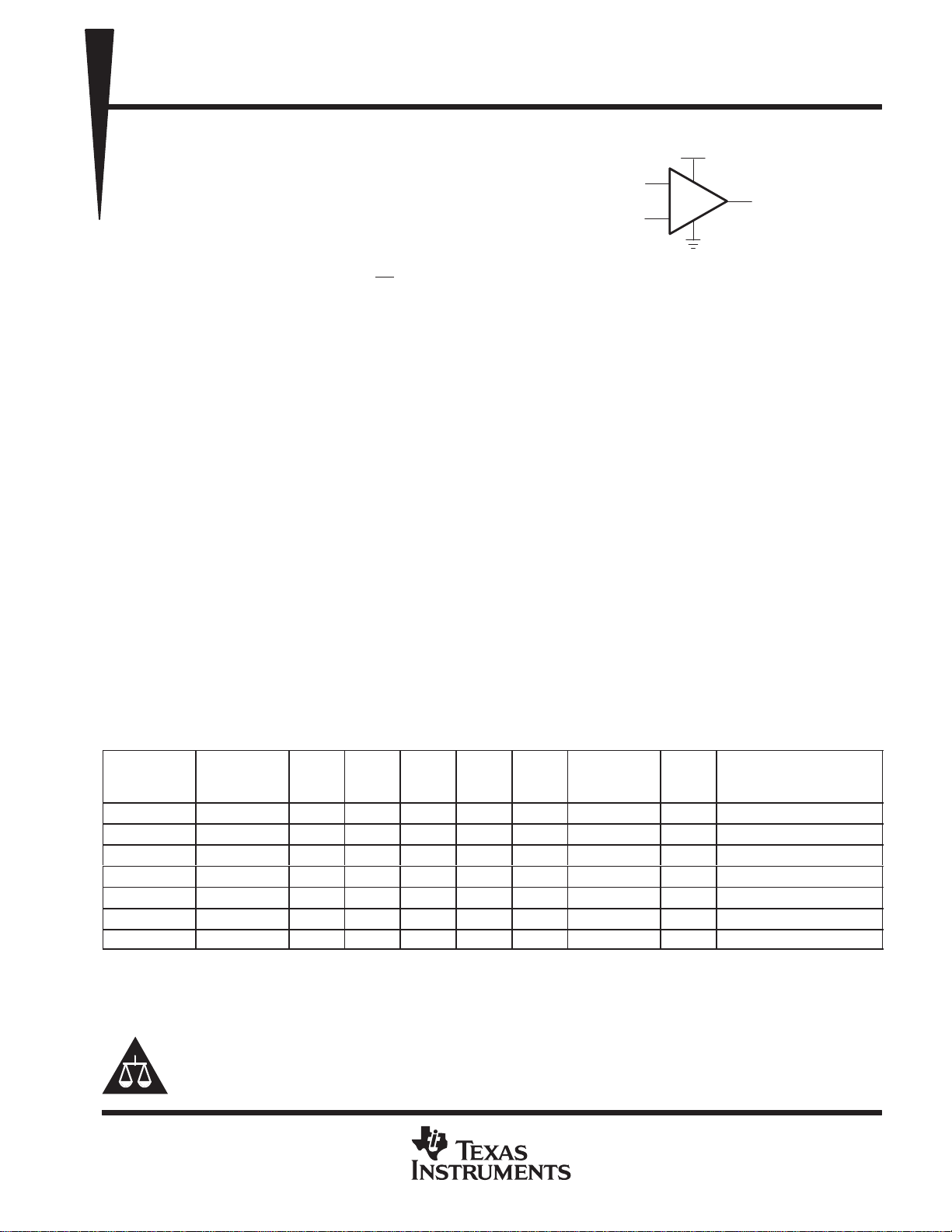
D Rail-To-Rail Input/Output
D Wide Bandwidth ...3 MHz
D High Slew Rate . . . 2.4 V/µs
Operational Amplifier
−
D Supply Voltage Range . . . 2.7 V to 16 V
D Supply Current . . . 550 µA/Channel
+
D Low Power Shutdown Mode
I
DD(SHDN)
... 25 µA/Channel
D Input Noise Voltage . . . 39 nV/√Hz
D Input Bias Current...1 pA
D Specified Temperature Range
−40°C to 125°C . . . Industrial Grade
D Ultrasmall Packaging
− 5 or 6 Pin SOT-23 (TLV2370/1)
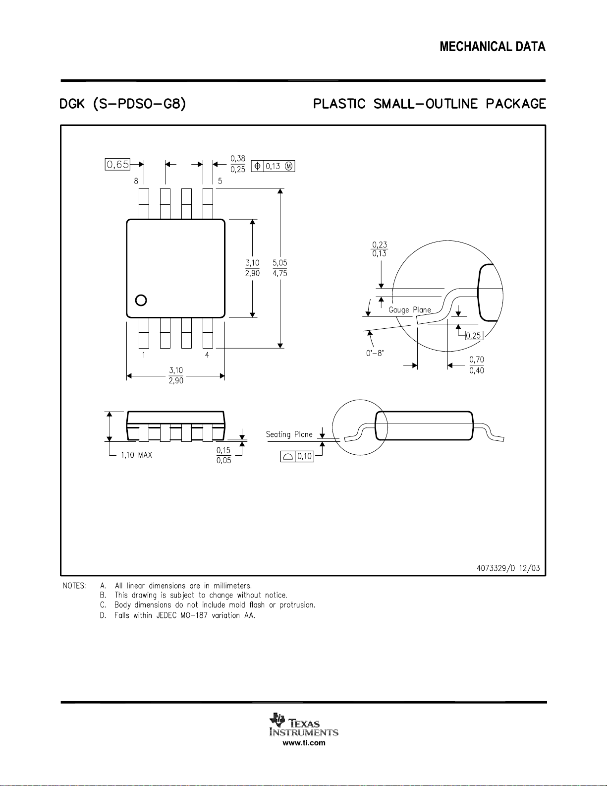
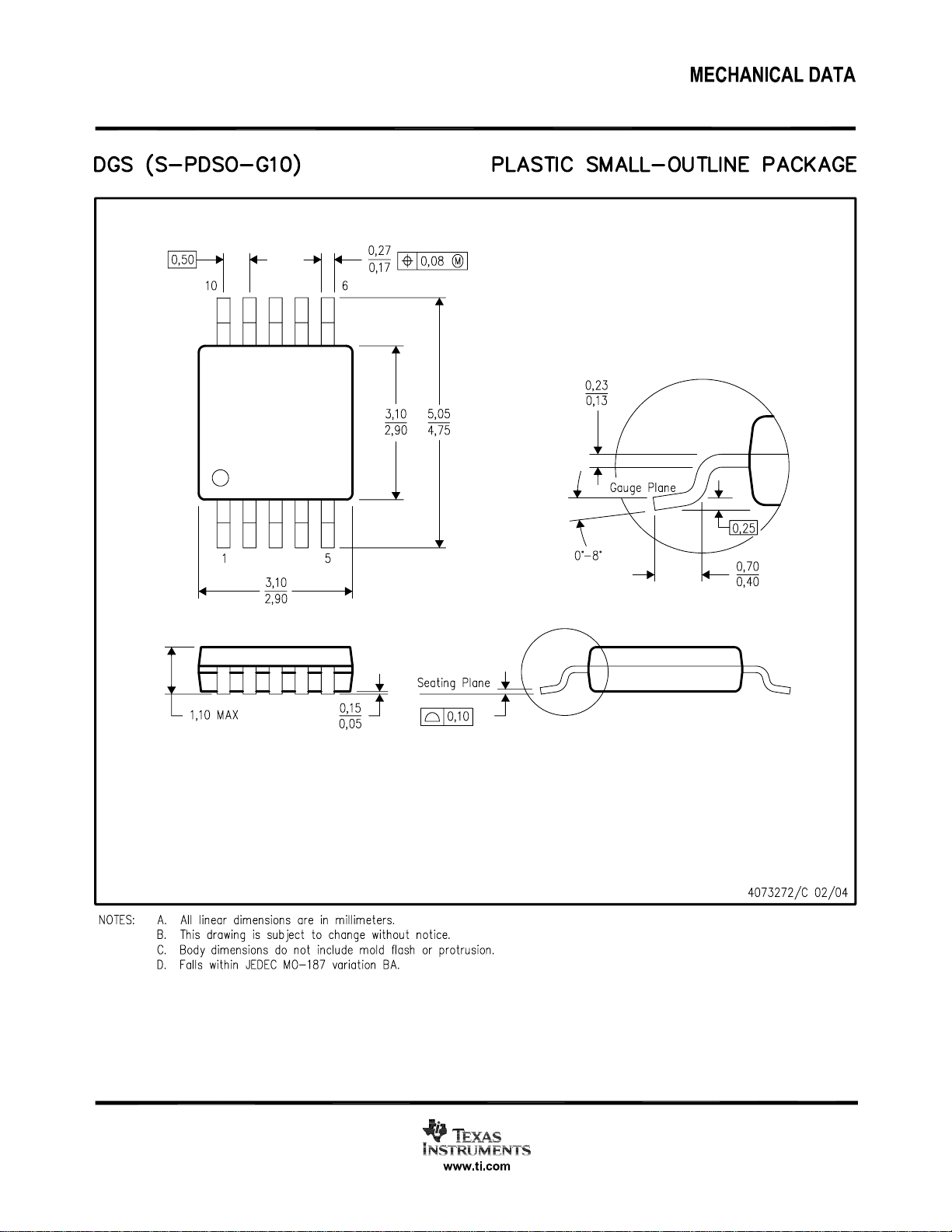
− 8 or 10 Pin MSOP (TLV2372/3)
description
The TLV237x single supply operational amplifiers provide rail-to-rail input and output capability . The TLV237x
takes the minimum operating supply voltage down to 2.7 V over the extended industrial temperature range while
adding the rail-to-rail output swing feature. The TLV237x also provides 3-MHz bandwidth from only 550 µA. The
maximum recommended supply voltage is 16 V, which allows the devices to be operated from (±8 V supplies
down to ±1.35 V) a variety of rechargeable cells.
The CMOS inputs enable use in high-impedance sensor interfaces, with the lower voltage operation making
an ideal alternative for the TLC227x in battery-powered applications. The rail-to-rail input stage further
increases its versatility. The TLV237x is the seventh member of a rapidly growing number of RRIO products
available from TI, and it is the first to allow operation up to 16-V rails with good ac performance.
All members are available in PDIP and SOIC with the singles in the small SOT-23 package, duals in the MSOP,
and quads in the TSSOP package.
The 2.7-V operation makes the TLV237x compatible with Li-Ion powered systems and the operating supply
voltage range of many micro-power microcontrollers available today including TI’s MSP430.
SELECTION OF SIGNAL AMPLIFIER PRODUCTS
DEVICE
TLV237x 2.7−16 500 550 1 3 2.4 Yes I/O S/D/Q
TLC227x 4−16 300 1100 1 2.2 3.6 — O D/Q
TLV27x 2.7−16 500 550 1 3 2.4 — O S/D/Q
TLC27x 3−16 1100 675 1 1.7 3.6 — — S/D/Q
TLV246x 2.7−6 150 550 1300 6.4 1.6 Yes I/O S/D/Q
TLV247x 2.7−6 250 600 2 2.8 1.5 Yes I/O S/D/Q
TLV244x 2.7−10 300 725 1 1.8 1.4 — O D/Q
†
Typical values measured at 5 V, 25°C
VDD (V)
V
(µV)
IO
Iq/Ch
(µA)
IIB (pA)
GBW
(MHz)SR(V/µs)
SHUTDOWN
†
RAIL-
TO-
RAIL
SINGLES/DUALS/QUADS
Please be aware that an important notice concerning availability, standard warranty, and use in critical applications o
Texas Instruments semiconductor products and disclaimers thereto appears at the end of this data sheet.
!"#$%&'(!$" !) *+%%,"( ') $# -+./!*'(!$" 0'(,1
%$0+*() *$"#$%& ($ )-,*!#!*'(!$") -,% (, (,%&) $# ,2') ")(%+&,"()
)('"0'%0 3'%%'"(41 %$0+*(!$" -%$*,))!"5 0$,) "$( ",*,))'%!/4 !"*/+0,
(,)(!"5 $# '// -'%'&,(,%)1
POST OFFICE BOX 1443
WWW.TI.COM
• HOUSTON, TEXAS 77251−1443
Copyright 2001 − 2003, Texas Instruments Incorporated
1
Page 2
NUMBER OF
UNIVERSAL
DEVICE
NUMBER OF
SHUTDOWN
UNIVERSAL
Selection Guide
(Lit# SLOU060)
(Lit# SLOU060)
A
SMALL OUTLINE
PLASTIC DIP
T
A
25°C
SMALL OUTLINE
PLASTIC DIP
A
T
A
25°C
OUTLINE
DIP
DIP
µ
SLOS270C − MARCH 2001 − REVISED DECEMBER 2003
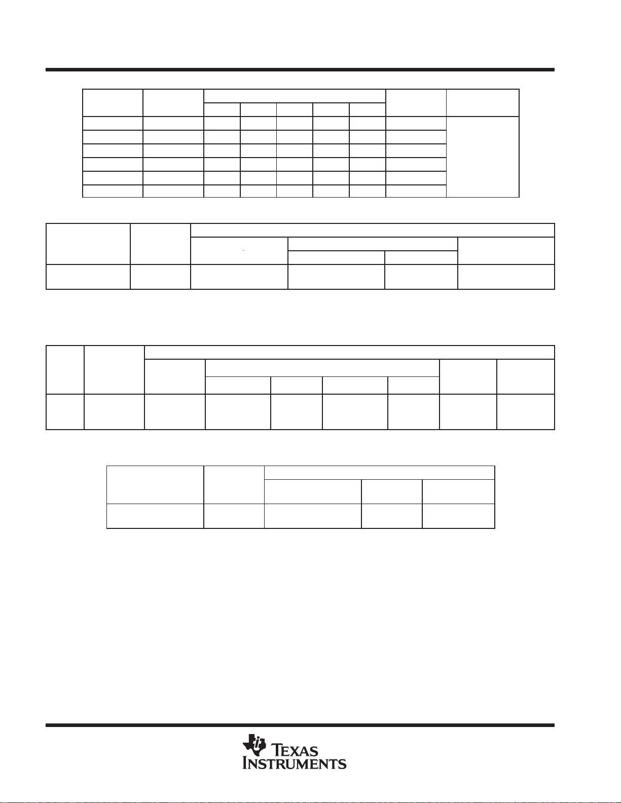
FAMILY PACKAGE TABLE
PACKAGE TYPES
CHANNELS
TLV2370 1 8 8 6 — — Yes
TLV2371 1 8 8 5 — — —
TLV2372 2 8 8 — — 8 —
TLV2373 2 14 14 — — 10 Yes
TLV2374 4 14 14 — 14 — —
TLV2375 4 16 16 — 16 — Yes
T
−40°C to 125°C 4.5 mV
†
This package is available taped and reeled. To order this packaging option, add an R suffix to the part number (e.g., TLV2370IDR).
‡
This package is only available taped and reeled. For standard quantities (3,000 pieces per reel), add an R suffix (e.g., TLV2370IDBVR). For
smaller quantities (250 pieces per mini-reel), add a T suffix to the part number (e.g., TLV2370IDBVT).
VIOMAX AT
°
PDIP SOIC SOT-23 TSSOP MSOP
TLV2370 and TLV2371 AVAILABLE OPTIONS
PACKAGED DEVICES
SOT-23
‡
(D)
TLV2370ID
TLV2371ID
†
(DBV)
TLV2370IDBV
TLV2371IDBV
SYMBOL
VBFI
VBGI
EVM BOARD
Refer to the EVM
(P)
TLV2370IP
TLV2371IP
TLV2372 AND TLV2373 AVAILABLE OPTIONS
PACKAGED DEVICES
to
VIOMAX AT
°
4.5 mV
−40°C to 125°C 4.5 mV
¶
This package is available taped and reeled. To order this packaging option, add an R suffix to the part number
(e.g., TL V2374IDR).
T
−40°C
125°C
§
This package is available taped and reeled. To order this packaging option, add an R suffix to the part number (e.g., TLV2372IDR).
SMALL
(D)
TLV2372ID
TLV2373ID
T
A
MSOP
§
TLV2372IDGK
TLV2374 and TLV2375 AVAILABLE OPTIONS
VIOMAX AT
(DGK)
—
25°C
§
SYMBOL (DGS)
APG
—
SMALL OUTLINE
TLV2374ID
TLV2375ID
(D)
¶
TLV2373IDGS
§
—
PACKAGED DEVICES
SYMBOL
—
API
PLASTIC DIP
(N)
TLV2374IN
TLV2375IN
PLASTIC
(N)
—
TLV2373IN
TSSOP
¶
(PW)
TLV2374IPW
TLV2375IPW
PLASTIC
(P)
TLV2372IP
—
2
POST OFFICE BOX 1443
WWW.TI.COM
• HOUSTON, TEXAS 77251−1443
Page 3
µ
SLOS270C − MARCH 2001 − REVISED DECEMBER 2003
TLV2370
DBV PACKAGE
(TOP VIEW)
8
7
6
5
14
13
12
11
10
V
6
5
4
DD
SHDN
IN−
NC
V
DD
OUT
NC
V
DD
2OUT
2IN−
2IN+
NC
2SHDN
9
8
NC
OUT
GND
IN+
NC
IN−
IN+
GND
1OUT
1IN−
1IN+
GND
NC
1SHDN
NC
NC − No internal connection
(1) SOT−23 may or may not be indicated
1
2
3
TLV2371
D OR P PACKAGE
(TOP VIEW)
1
2
3
4
TLV2373
D OR N PACKAGE
(TOP VIEW)
1
2
3
4
5
6
7
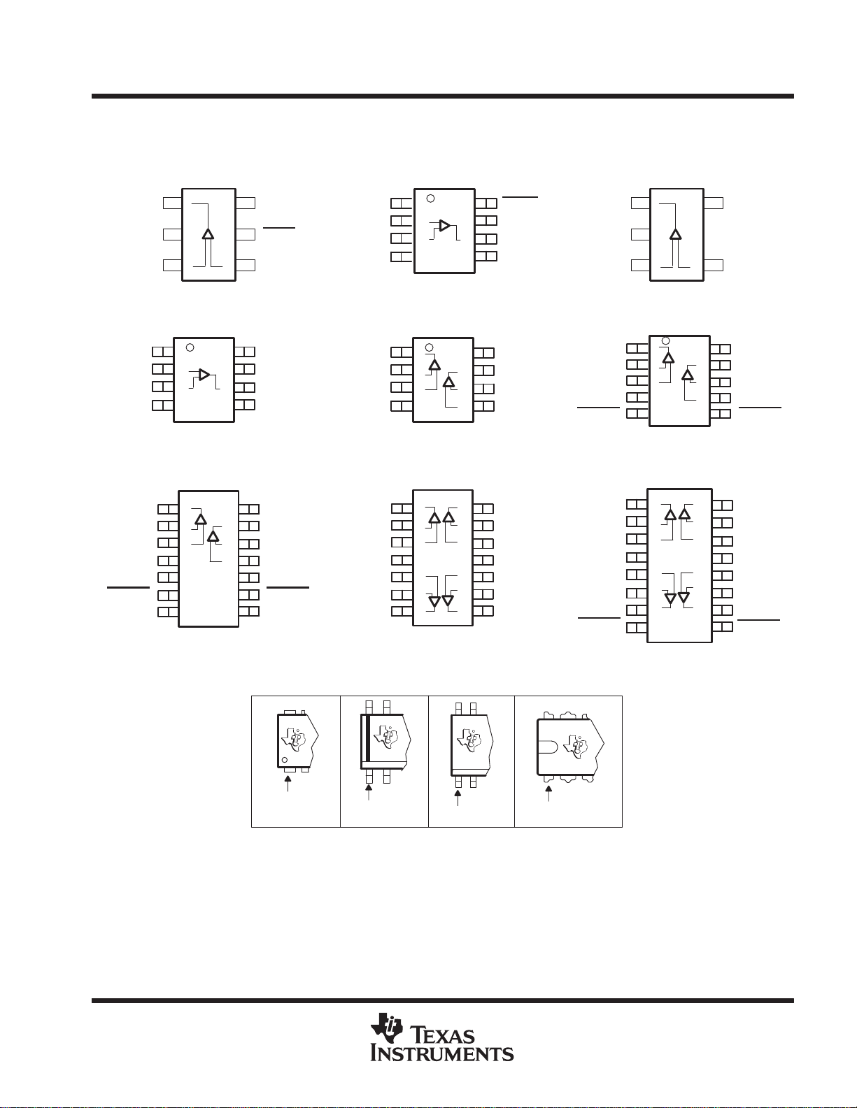
TLV237x PACKAGE PINOUTS
TLV2370
D OR P PACKAGE
(TOP VIEW)
NC
IN−
IN+
GND
D, DGK, OR P PACKAGE
1OUT
1IN−
1IN+
GND
1OUT
1IN−
1IN+
V
DD
2IN+
2IN−
2OUT
1
2
3
4
TLV2372
(TOP VIEW)
1
2
3
4
TLV2374
D, N, OR PW PACKAGE
(TOP VIEW)
1
2
3
4
5
6
7
14
13
12
11
10
SHDN
8
V
7
6
5
8
7
6
5
DD
OUT
NC
V
DD
2OUT
2IN−
2IN+
4OUT
4IN−
4IN+
GND
3IN+
9
3IN−
8
3OUT
(1)
DBV PACKAGE
(TOP VIEW)
OUT
GND
IN+
1OUT
1IN−
1IN+
GND
1SHDN
1OUT
1IN−
1IN+
V
DD
2IN+
2IN−
2OUT
1SHDN
1
2
3
DGS PACKAGE
(TOP VIEW)
1
2
3
4
5
TLV2375
D, N, OR PW PACKAGE
(TOP VIEW)
1
2
3
+
4
5
6
7
8
TLV2371
TLV2373
5
4
10
16
15
14
13
12
11
10
V
DD
IN−
V
DD
2OUT
9
2IN−
8
2IN+
7
2SHDN
6
4OUT
4IN−
4IN+
GND
3IN+
3IN−
3OUT
9
2SHDN
Pin 1
Printed or
Molded Dot
TYPICAL PIN 1 INDICATORS
Pin 1
Stripe
POST OFFICE BOX 1443
WWW.TI.COM
• HOUSTON, TEXAS 77251−1443
Pin 1
Bevel Edges
Pin 1
Molded ”U” Shape
3
Page 4
µ
SLOS270C − MARCH 2001 − REVISED DECEMBER 2003
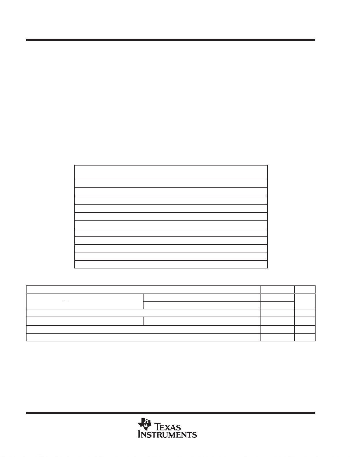
absolute maximum ratings over operating free-air temperature range (unless otherwise noted)
Supply voltage, V
Differential input voltage, V
Input voltage range, V
Input current range, I
Output current range, I
Continuous total power dissipation See Dissipation Rating Table. . . . . . . . . . . . . . . . . . . . . . . . . . . . . . . . . . . . .
Operating free-air temperature range, T
Maximum junction temperature, T
Storage temperature range, T
Lead temperature 1,6 mm (1/16 inch) from case for 10 seconds 260°C. . . . . . . . . . . . . . . . . . . . . . . . . . . . . . .
†
Stresses beyond those listed under “absolute maximum ratings” may cause permanent damage to the device. These are stress ratings only , a nd
functional operation of the device at these or any other conditions beyond those indicated under “recommended operating conditions” is not
implied. Exposure to absolute-maximum-rated conditions for extended periods may affect device reliability.
NOTE 1: All voltage values, except differential voltages, are with respect to GND.
(see Note 1) 16.5 V. . . . . . . . . . . . . . . . . . . . . . . . . . . . . . . . . . . . . . . . . . . . . . . . . . . . . . . . . .
DD
I
±10 mA. . . . . . . . . . . . . . . . . . . . . . . . . . . . . . . . . . . . . . . . . . . . . . . . . . . . . . . . . . . . . . . . . . . .
I
PACKAGE
D (8) 38.3 176 710 mW
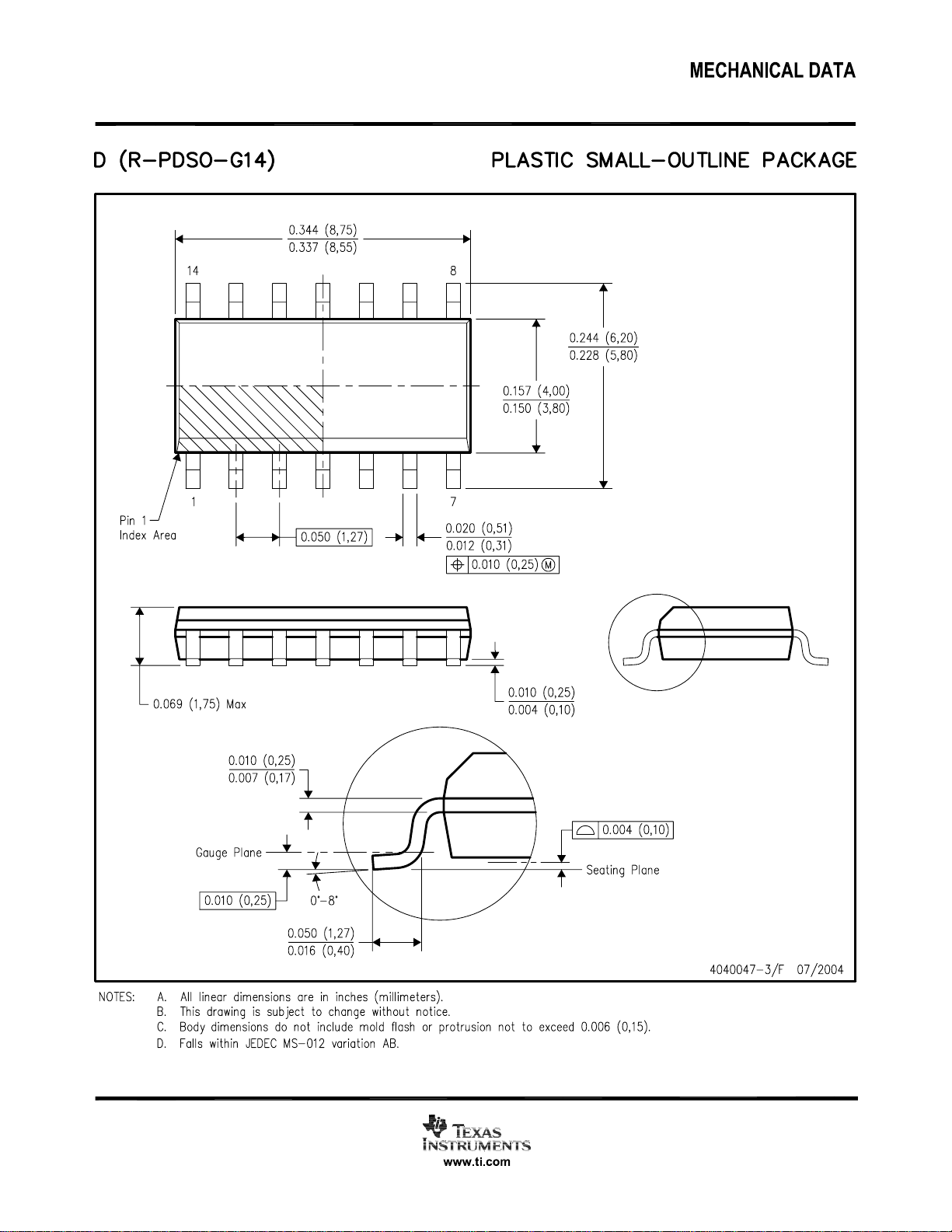
D (14) 26.9 122.3 1022 mW
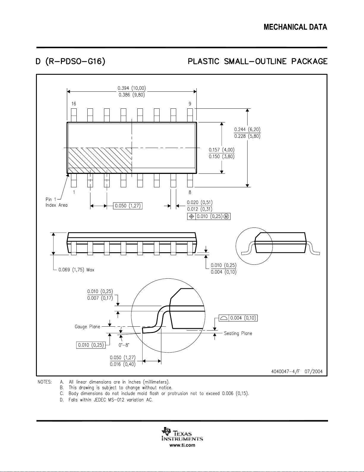
D (16) 25.7 114.7 1090 mW
DBV (5) 55 324.1 385 mW
DBV (6) 55 294.3 425 mW
DGK (8) 54.23 259.96 481 mW
DGS (10) 54.1 257.71 485 mW
N (14, 16) 32 78 1600 mW
P (8) 41 104 1200 mW
PW (14) 29.3 173.6 720 mW
PW (16) 28.7 161.4 774 mW
±V
. . . . . . . . . . . . . . . . . . . . . . . . . . . . . . . . . . . . . . . . . . . . . . . . . . . . . . . . . . . . . .
ID
(see Note 1) −0.2 V to VDD + 0.2 V. . . . . . . . . . . . . . . . . . . . . . . . . . . . . . . . . . . . . . . . . . .
±100 mA. . . . . . . . . . . . . . . . . . . . . . . . . . . . . . . . . . . . . . . . . . . . . . . . . . . . . . . . . . . . . . . .
O
: I suffix −40°C to 125°C. . . . . . . . . . . . . . . . . . . . . . . . . . . . . . . . . . . .
A
150°C. . . . . . . . . . . . . . . . . . . . . . . . . . . . . . . . . . . . . . . . . . . . . . . . . . . . . . . . .
J
−65°C to 150°C. . . . . . . . . . . . . . . . . . . . . . . . . . . . . . . . . . . . . . . . . . . . . . . . . . .
stg
DISSIPATION RATING TABLE
θ
JC
(°C/W)
θ
JA
(°C/W)
TA ≤ 25°C
POWER RATING
†
DD
recommended operating conditions
Supply voltage, V
Common-mode input voltage range, V
Operating free-air temperature, T
Turnon voltage level, V
Turnoff voltage level, V
4
DD
ICR
A
, relative to GND pin voltage 2 V
(ON)
, relative to GND pin voltage 0.8 V
(OFF)
POST OFFICE BOX 1443
MIN MAX UNIT
Single supply 2.7 16
Split supply ±1.35 ±8
0 V
DD
I-suffix −40 125 °C
WWW.TI.COM
• HOUSTON, TEXAS 77251−1443
V
V
Page 5
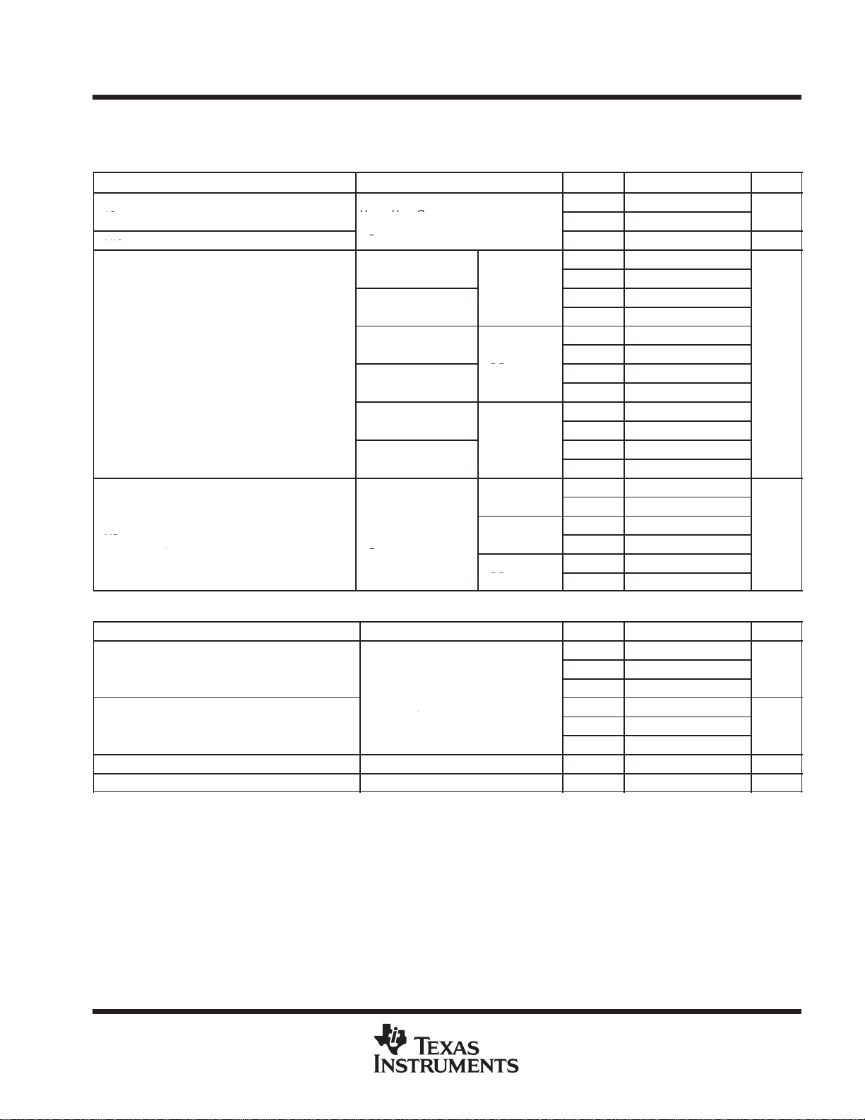
RS = 50 Ω
VIO
RS = 50
V
= 0 to V
,
VIC = 0 to VDD,
V
= 0 to V
−1.35V,
VIC = 0 to VDD−1.35V,
V
= 0 to V
,
VIC = 0 to VDD,
V
= 0 to V
−1.35V,
VIC = 0 to VDD−1.35V,
V
= 0 to V
,
VIC = 0 to VDD,
V
= 0 to V
−1.35V,
VIC = 0 to VDD−1.35V,
Large-signal differential voltage
V
= V
/2,
Large-signal differential voltage
V
O(PP)
= VDD/2,
amplification
RL = 10 k
IO
IIOInput offset current
V
= 15 V, V
= V
/2,
pA
VDD = 15 V, VIC = VDD/2,
IB
VO = VDD/2
IIBInput bias current
pA
µ
SLOS270C − MARCH 2001 − REVISED DECEMBER 2003
electrical characteristics at specified free-air temperature, VDD = 2.7 V, 5 V, and 15 V (unless
otherwise noted)
dc performance
PARAMETER TEST CONDITIONS
V
IO
α
CMRR Common-mode rejection ratio
A
VD
Input offset voltage
Offset voltage drift
amplification
VIC = VDD/2,
RS = 50 Ω
RS = 50 Ω
RS = 50 Ω,
RS = 50 Ω,
RS = 50 Ω,
RS = 50 Ω,
RL = 10 kΩ
VO = VDD/2,
VDD = 2.7 V
VDD = 5 V
VDD = 15 V
VDD = 2.7 V
VDD = 5 V
VDD = 15 V
T
A
25°C 2 4.5
Full range
25°C 2 µV/°C
25°C 50 68
Full range 49
25°C 56 70
Full range 54
25°C 55 72
Full range 54
25°C 67 80
Full range 64
25°C 64 82
Full range 63
25°C 67 84
Full range 66
25°C 98 106
Full range 76
25°C 100 110
Full range 86
25°C 81 83
Full range 79
MIN TYP MAX
UNIT
mV
6
dB
dB
input characteristics
PARAMETER TEST CONDITIONS T
I
I
r
C
i(d)
IC
Input offset current
Input bias current
Differential input resistance 25°C 1000 GΩ
Common-mode input capacitance f = 21 kHz 25°C 8 pF
VO = VDD/2
A
25°C 1 60
70°C 100
125°C 1000
25°C 1 60
70°C 100
125°C 1000
MIN TYP MAX UNIT
pA
pA
POST OFFICE BOX 1443
WWW.TI.COM
• HOUSTON, TEXAS 77251−1443
5
Page 6
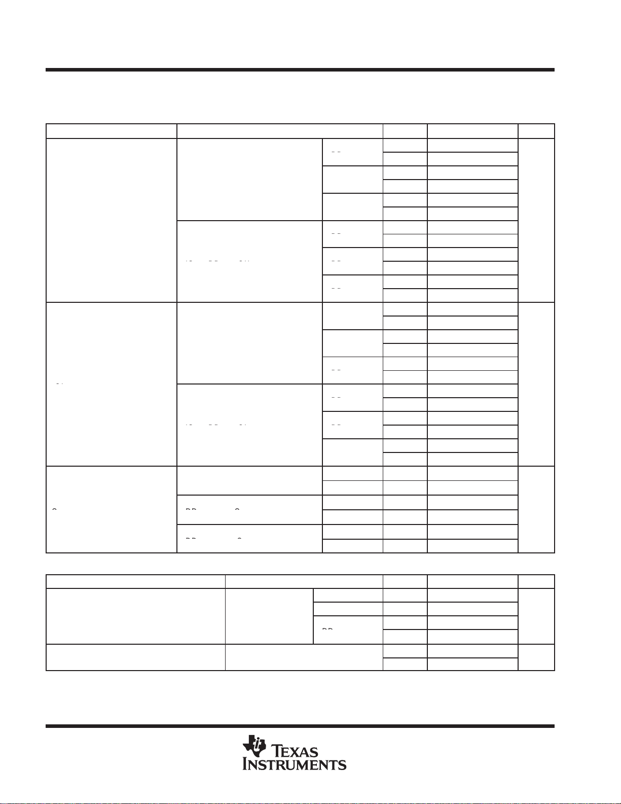
VDD = 2.7 V, VO = 0.5 V from rail
IOOutput current
VDD = 5 V, VO = 0.5 V from rail
mA
VDD = 15 V, VO = 0.5 V from rail
IDDSupply current (per channel)
VO = VDD/2,
A
VDD = 15 V
Supply voltage rejection ratio
V
= 2.7 V to 15 V,
V
= V
/2,
Supply voltage rejection ratio
VDD = 2.7 V to 15 V,
VIC = VDD/2,
µ
SLOS270C − MARCH 2001 − REVISED DECEMBER 2003
electrical characteristics at specified free-air temperature, VDD = 2.7 V, 5 V, and 15 V (unless
otherwise noted) (continued)
output characteristics
PARAMETER TEST CONDITIONS
V
High-level output voltage
OH
V
Low-level output voltage
OL
VDD = 2.7 V
VIC = VDD/2, IOH = −1 mA VDD = 5 V
VDD = 15 V
VDD = 2.7 V
VIC = VDD/2, IOH = −5 mA VDD = 5 V
VDD = 15 V
VDD = 2.7 V
VIC = VDD/2, IOL = 1 mA VDD = 5 V
VDD = 15 V
VDD = 2.7 V
VIC = VDD/2, IOL = 5 mA VDD = 5 V
VDD = 15 V
Positive rail 25°C 4
Negative rail 25°C 5
Positive rail 25°C 7
Negative rail 25°C 8
Positive rail 25°C 16
Negative rail 25°C 15
T
A
25°C 2.55 2.58
Full range 2.48
25°C 4.9 4.93
Full range 4.85
25°C 14.92 14.96
Full range 14.9
25°C 1.9 2
Full range 1.6
25°C 4.6 4.68
Full range 4.5
25°C 14.7 14.8
Full range 14.6
25°C 0.1 0.15
Full range 0.22
25°C 0.05 0.1
Full range 0.15
25°C 0.05 0.08
Full range 0.1
25°C 0.52 0.7
Full range 1.1
25°C 0.28 0.4
Full range 0.5
25°C 0.19 0.3
Full range 0.35
MIN TYP MAX
UNIT
V
V
power supply
PARAMETER TEST CONDITIONS T
PSRR
6
(∆VDD /∆VIO)
No load
POST OFFICE BOX 1443
VDD = 2.7 V 25°C 470 560
VDD = 5 V 25°C 550 660
WWW.TI.COM
• HOUSTON, TEXAS 77251−1443
A
25°C 750 900
Full range 1200
25°C 70 80
Full range 65
MIN TYP MAX UNIT
µ
dB
Page 7
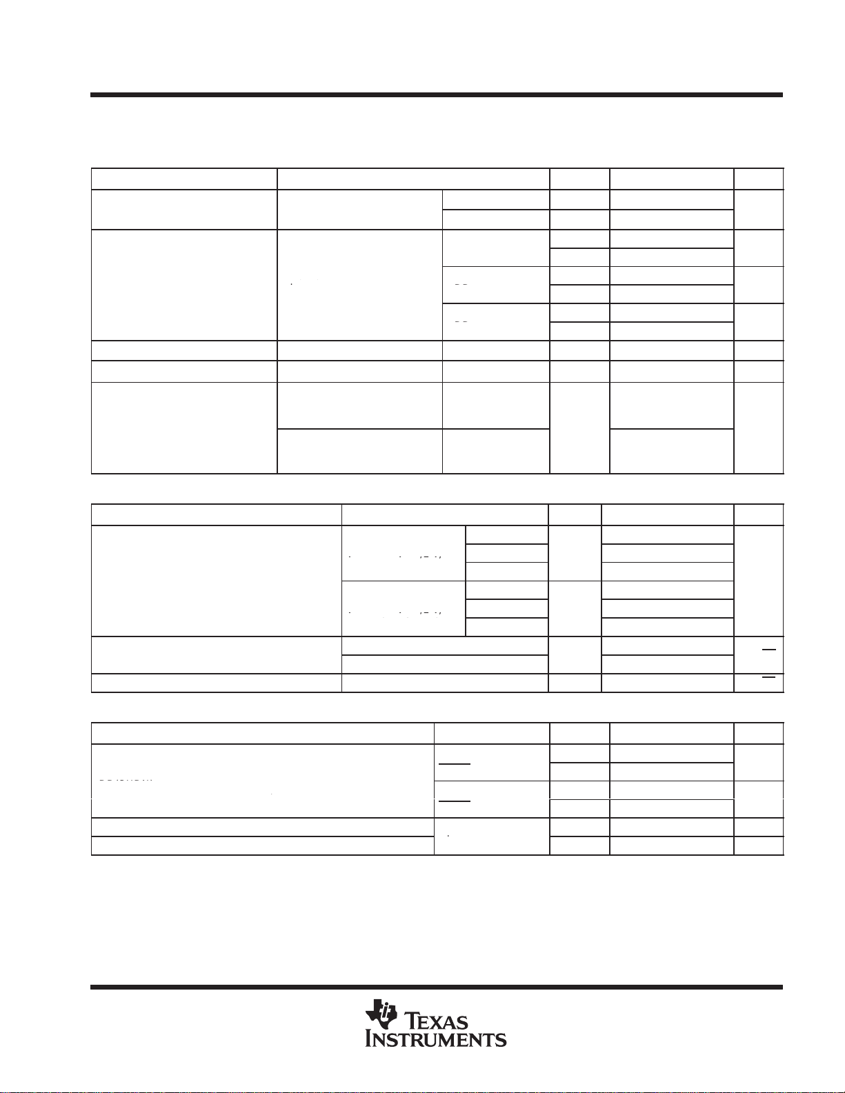
R
= 2 kΩ,
RL = 2 kΩ
O(PP) DD
C
= 50 pF,
R
= 10 k
RL = 10 kΩ
VDD = 2.7 V,
O(PP)
V
O(PP)
= VDD/2 V,
25 C
VDD = 5 V, 15 V,
O(PP)
V
O(PP)
= VDD/2 V,
25 C
nV/√Hz
V
= 2.7 V, 5 V,
Supply current in shutdown mode (TLV2370,
VDD = 2.7 V, 5 V,
)
Supply current in shutdown mode (TLV2370,
V
= 15 V,
TLV2373, TLV2375) (per channel)
VDD = 15 V,
RL = 2 k
µ
SLOS270C − MARCH 2001 − REVISED DECEMBER 2003
electrical characteristics at specified free-air temperature, VDD = 2.7 V, 5 V, and 15 V (unless
otherwise noted) (continued)
dynamic performance
PARAMETER TEST CONDITIONS
UGBW Unity gain bandwidth
SR Slew rate at unity gain
φ
m
t
s
Phase margin
Gain margin
Settling time
CL = 10 pF
V
O(PP)
L
RL = 2 kΩ, CL = 100 pF
RL = 2 kΩ, CL = 10 pF
VDD = 2.7 V,
V
(STEP)PP
CL = 10 pF, RL = 2 kΩ
VDD = 5 V, 15 V,
V
(STEP)PP
CL = 47 pF, RL = 2 kΩ
,
= VDD/2,
Ω
= 1 V, AV = −1,
= 1 V, AV = −1,
VDD = 2.7 V
VDD = 5 V to 15 V
VDD = 2.7 V
VDD = 5 V
VDD = 15 V
0.1%
0.1%
T
A
25°C 2.4
25°C 3
25°C
Full range 1
25°C
Full range 1.2
25°C
Full range 1.4
25°C 65°
25°C 18 dB
25°C
MIN TYP MAX UNIT
MHz
1.4 2
1.6 2.4
1.9 2.1
2.9
2
V/µs
V/µs
V/µs
µs
noise/distortion performance
PARAMETER TEST CONDITIONS
THD + N Total harmonic distortion plus noise
V
n
I
n
Equivalent input noise voltage
Equivalent input noise current f = 1 kHz 25°C 0.6
V
= VDD/2 V,
RL = 2 kΩ, f = 10 kHz
V
= VDD/2 V,
RL = 2 kΩ, f = 10 kHz
f = 1 kHz
f = 10 kHz
T
A
AV = 1 0.02%
AV = 10
AV = 100
AV = 1 0.02%
AV = 10
AV = 100
25°C
25°C
25°C
MIN TYP MAX UNIT
0.05%
0.18%
0.09%
0.5%
39
35
fA/√Hz
shutdown characteristics
PARAMETER TEST CONDITIONS
I
DD(SHDN
t
(on)
t
(off)
NOTE 2: Disable time and enable time are defined as the interval between application of the logic signal to the SHDN terminal and the point at
TLV2373, TLV2375) (per channel)
Amplifier turnon time (see Note 2)
Amplifier turnoff time (see Note 2)
which the supply current has reached one half of its final value.
SHDN = 0 V
SHDN = 0 V
Ω
T
A
25°C 25 30
Full range 35
25°C 40 45
Full range 50
25°C 0.8 µs
25°C 1 µs
MIN TYP MAX UNIT
µA
µA
POST OFFICE BOX 1443
WWW.TI.COM
• HOUSTON, TEXAS 77251−1443
7
Page 8
µ
SLOS270C − MARCH 2001 − REVISED DECEMBER 2003
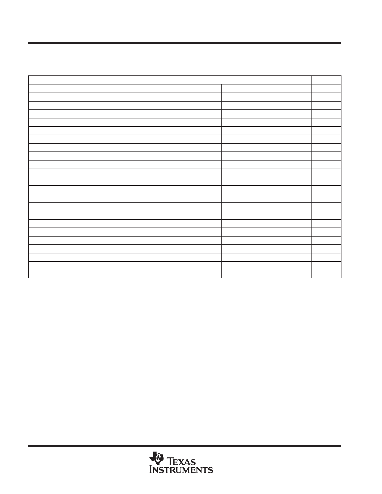
TYPICAL CHARACTERISTICS
Table of Graphs
FIGURE
V
IO
CMRR Common-mode rejection ratio vs Frequency 4
V
OL
V
OH
V
O(PP)
I
DD
PSRR Power supply rejection ratio vs Frequency 14
A
VD
SR Slew rate
φ
m
V
n
I
DD(SHDN)
I
DD(SHDN)
I
DD(SHDN)
Input offset voltage vs Common-mode input voltage 1, 2, 3
Input bias and offset current vs Free-air temperature 5
Low-level output voltage vs Low-level output current 6, 8, 10
High-level output voltage vs High-level output current 7, 9, 11
Peak-to-peak output voltage vs Frequency 12
Supply current vs Supply voltage 13
Differential voltage gain & phase vs Frequency 15
Gain-bandwidth product vs Free-air temperature 16
vs Supply voltage 17
vs Free-air temperature
Phase margin vs Capacitive load 19
Equivalent input noise voltage vs Frequency 20
Voltage-follower large-signal pulse response 21, 22
Voltage-follower small-signal pulse response 23
Inverting large-signal response 24, 25
Inverting small-signal response 26
Crosstalk vs Frequency 27
Shutdown forward & reverse isolation vs Frequency 28
Shutdown supply current vs Supply voltage 29
Shutdown pin leakage current vs Shutdown pin voltage 30
Shutdown supply current/output voltage vs Time 31, 32
18
8
POST OFFICE BOX 1443
WWW.TI.COM
• HOUSTON, TEXAS 77251−1443
Page 9
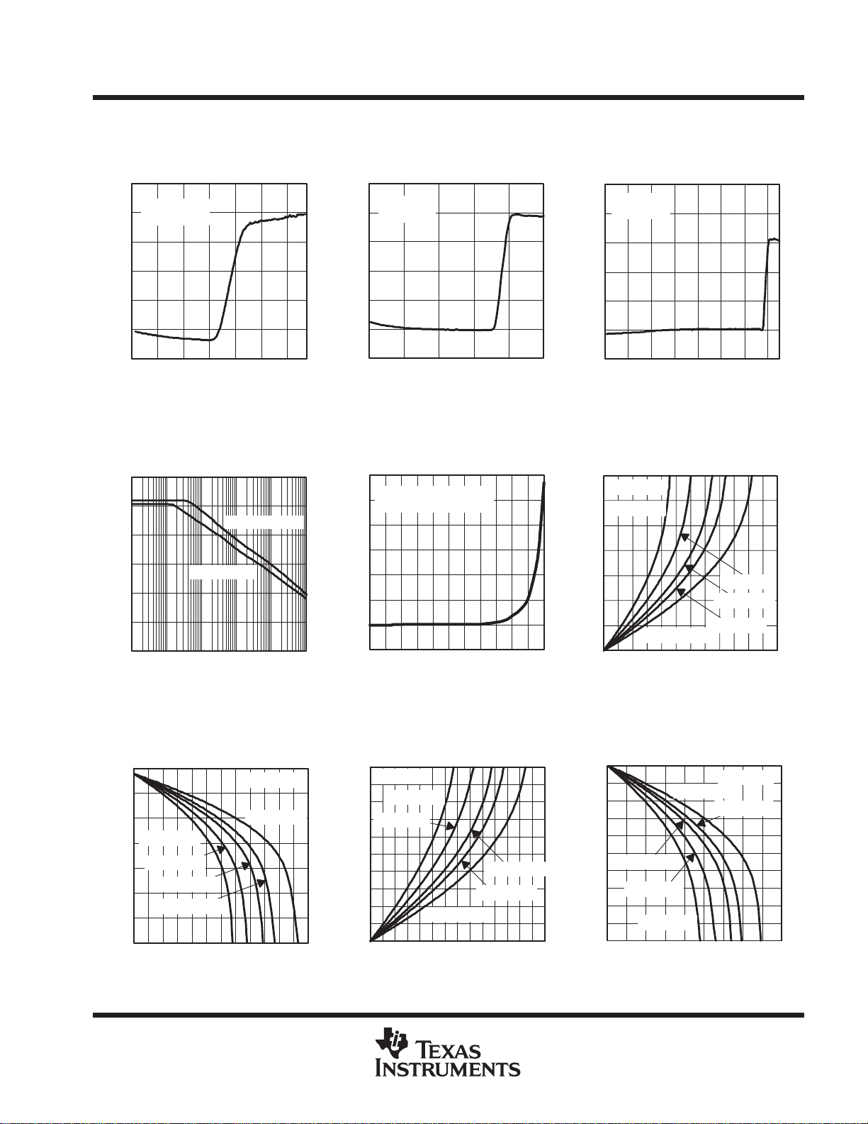
INPUT OFFSET VOLTAGE
µ
SLOS270C − MARCH 2001 − REVISED DECEMBER 2003
TYPICAL CHARACTERISTICS
INPUT OFFSET VOLTAGE
vs
COMMON-MODE INPUT VOLTAGE
1000
VDD = 2.7 V
800
µ
− Input Offset Voltage − V
IO
V
TA = 25°C
600
400
200
0
−200
0 0.4 0.8 1.2 1.6 2 2.4 2.7
V
− Common-Mode Input Voltage − V
ICR
Figure 1
COMMON-MODE REJECTION RATIO
vs
120
100
80
60
40
20
0
CMRR − Common-Mode Rejection Ratio − dB
10
FREQUENCY
VDD = 2.7 V
100 1 k
f − Frequency − Hz
VDD = 5 V, 15 V
100 k
10 k
Figure 4
COMMON-MODE INPUT VOLTAGE
1000
800
µ
600
400
200
− Input Offset Voltage − V
0
IO
V
−200
012345
V
ICR
INPUT BIAS/OFFSET CURRENT
300
250
200
150
100
50
− Input Bias / Offset Current − pA
IO
I
0
/
IB
I
−50
1 M
−40−25 −10 5 20 35 50 65 80 95 110 125
INPUT OFFSET VOLTAGE
vs
VDD = 5 V
TA = 25 °C
− Common-Mode Input Voltage − V
Figure 2
vs
FREE-AIR TEMPERATURE
VDD = 2.7 V, 5 V and 15 V
VIC = VDD/2
TA − Free-Air Temperature − °C
Figure 5
COMMON-MODE INPUT VOLTAGE
vs
1000
VDD =15 V
TA = 25 °C
800
µ
600
400
200
− Input Offset Voltage − V
0
IO
V
−200
0246810121415
V
− Common-Mode Input Voltage −V
ICR
Figure 3
LOW-LEVEL OUTPUT VOLTAGE
vs
LOW-LEVEL OUTPUT CURRENT
2.80
VDD = 2.7 V
2.40
TA = 125 °C
2
1.60
1.20
0.80
0.40
OL
V − Low-Level Output Voltage − V
0
0 2 4 6 8 10 12 14 16 18 20 22 24
TA = 40 °C
IOL − Low-Level Output Current − mA
TA = 70 °C
TA = 25 °C
TA = 0 °C
Figure 6
HIGH-LEVEL OUTPUT VOLTAGE
HIGH-LEVEL OUTPUT CURRENT
2.80
2.40
2
TA = 125°C
1.60
− High-Level Output Voltage − V
OH
V
TA = 70°C
1.20
0.80
0.40
TA = 25°C
TA = 0°C
0
0123456789101112
IOH − High-Level Output Current − mA
vs
Figure 7
VDD = 2.7 V
TA =−40°C
LOW-LEVEL OUTPUT VOLTAGE
vs
LOW-LEVEL OUTPUT CURRENT
5
VDD = 5 V
4.50
TA = 125 °C
4
TA = 70 °C
3.50
3
2.50
2
1.50
1
OL
0.50
V − Low-Level Output Voltage − V
0
0 5 10 15 20 25 30 35 40 45 50 55 60 65 70
IOL − Low-Level Output Current − mA
TA = −40 °C
Figure 8
POST OFFICE BOX 1443
WWW.TI.COM
• HOUSTON, TEXAS 77251−1443
TA = 25 °C
TA = 0 °C
HIGH-LEVEL OUTPUT VOLTAGE
vs
HIGH-LEVEL OUTPUT CURRENT
5
4.50
4
3.50
3
2.50
TA = 25°C
2
1.50
− High-Level Output Voltage − V
OH
0.50
V
TA = 70°C
1
0
0 5 10 15 20 25 30 35 40 45
IOH − High-Level Output Current − mA
TA = −40°C
TA = 125°C
Figure 9
VCC = 5 V
TA = 0°C
9
Page 10
µ
SLOS270C − MARCH 2001 − REVISED DECEMBER 2003
TYPICAL CHARACTERISTICS
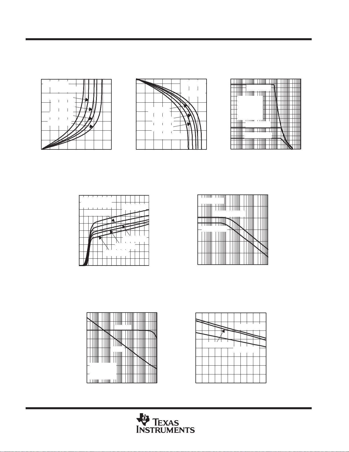
LOW-LEVEL OUTPUT VOLTAGE
vs
LOW-LEVEL OUTPUT CURRENT
15
VDD = 15 V
14
12
10
8
6
4
OL
2
V − Low-Level Output Voltage − V
0
0
TA =125°C
TA =70°C
TA =25°C
TA =0°C
TA =−40°C
20 40 60 80
IOL − Low-Level Output Current − mA
100 120 140 160
Figure 10
1
AV = 1
0.9
VIC = VDD / 2
0.8
0.7
0.6
0.5
0.4
0.3
0.2
DD
I Supply Current − − mA/Ch
0.1
0
0 1 2 3 4 5 6 7 8 9 10 11 12 13 14 15
SUPPLY CURRENT
vs
SUPPLY VOLTAGE
TA = 70°C
TA = 0°C
TA = −40°C
VCC − Supply Voltage − V
Figure 13
HIGH-LEVEL OUTPUT VOLTAGE
vs
HIGH-LEVEL OUTPUT CURRENT
15
14
12
10
8
6
4
− High-Level Output Voltage − V
2
OH
V
0
TA = 0°C
TA = 25°C
TA = 70°C
TA = 125°C
0 20 40 60 80 100 120 140 160
IOH − High-Level Output Current − mA
VDD = 15 V
Figure 11
TA = 125°C
TA = 25°C
PEAK-TO-PEAK OUTPUT VOLTAGE
16
TA = −40°C
15
14
13
12
11
10
9
8
7
6
5
4
− Peak-to-Peak Output Voltage − V
3
2
O(PP)
1
V
0
10 100 1 k 10 k 100 k 1 M 10 M
VDD = 15 V
AV = −10
RL = 2 kΩ
CL = 10 pF
TA = 25°C
THD = 5%
VDD = 5 V
VDD = 2.7 V
f − Frequency − Hz
POWER SUPPLY REJECTION RATIO
vs
FREQUENCY
120
TA = 25°C
100
80
60
40
20
PSRR − Power Supply Rejection Ratio − dB
0
10 100 1 k 10 k 100 k 1 M
VDD = 5 V, 15 V
VDD = 2.7 V
f − Frequency − Hz
Figure 14
vs
FREQUENCY
Figure 12
10
DIFFERENTIAL VOLTAGE GAIN AND PHASE
vs
VDD=5 Vdc
RL=2 kΩ
CL=10 pF
TA=25°C
f − Frequency − Hz
FREQUENCY
Phase
Gain
120
100
80
60
40
20
0
− Differential Voltage Gain − dB
−20
VD
A
−40
10 100 1 k 10 k 100 k 1 M 10 M
180
135
90
45
0
−45
−90
−135
−180
Figure 15
POST OFFICE BOX 1443
WWW.TI.COM
• HOUSTON, TEXAS 77251−1443
GAIN BANDWIDTH PRODUCT
FREE-AIR TEMPERATURE
4
3.5
3
2.5
VDD = 5 V
2
Phase − °
1.5
1
0.5
GBWP − Gain Bandwidth Product − MHz
0
−40−25 −10 5 20 35 50 65 80 95 110 125
vs
VDD = 15 V
VDD = 2.7 V
TA − Free-Air Temperature − °C
Figure 16
Page 11
µ
SLOS270C − MARCH 2001 − REVISED DECEMBER 2003
TYPICAL CHARACTERISTICS
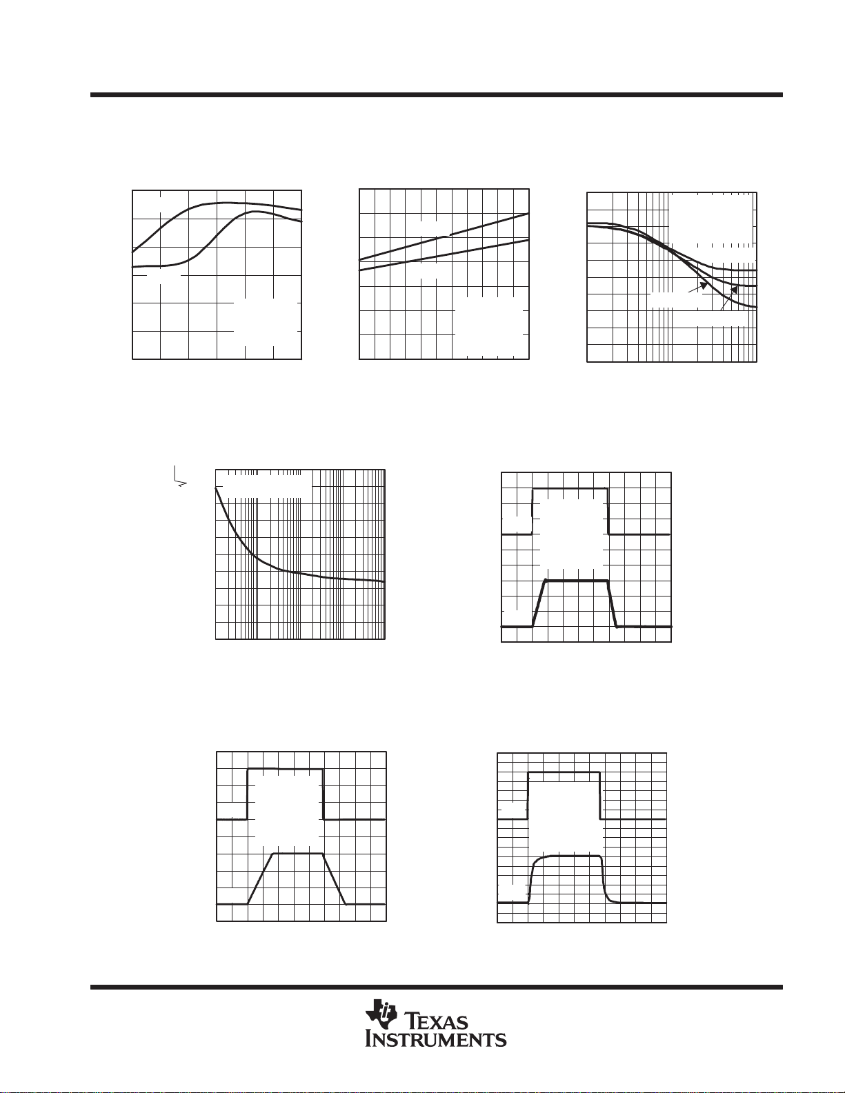
SLEW RATE
vs
SUPPLY VOLTAGE
3
SR−
2.5
s
µ
2
1.5
SR+
1
SR − Slew Rate − V/
0.5
0
2.5 4.5 6.5 8.5 10.5 12.5 14.5
VCC − Supply Voltage −V
AV = 1
RL = 10 kΩ
CL = 50 pF
TA = 25°C
Figure 17
EQUIVALENT INPUT NOISE VOLTAGE
100
VDD = 2.7, 5, 15 V
90
nV/ Hz− Equivalent Input Noise Voltage −V
TA = 25°C
80
70
60
50
40
30
20
10
0
n
10 100 1 k 10 k 100 k
vs
FREQUENCY
f − Frequency − Hz
Figure 20
SLEW RATE
vs
FREE-AIR TEMPERATURE
3.5
3
SR+
SR−
VDD = 5 V
AV = 1
RL = 10 kΩ
CL = 50 pF
VI = 3 V
s
2.5
µ
2
1.5
1
SR − Slew Rate − V/
0.5
0
−40 −25 −10 5 20 35 50 65 80 95 110 125
TA − Free-Air Temperature − °C
Figure 18
VOLTAGE-FOLLOWER LARGE-SIGNAL
4
3
2
1
0
− Input Voltage − V
I
V
PHASE MARGIN
100
90
80
70
60
50
40
Phase Margin − °
30
20
10
0
CAPACITIVE LOAD
10 100
CL − Capacitive Load − pF
PULSE RESPONSE
VDD = 5 V
AV = 1
V
I
RL = 2 kΩ
CL = 10 pF
VI = 3 V
PP
TA = 25°C
V
O
024681012141618
t − Time − µs
Figure 21
vs
VDD = 5 V
RL= 2 kΩ
TA = 25°C
AV = Open Loop
Rnull = 0
Figure 19
4
3
2
1
0
Rnull = 100
Rnull = 50
− Output Voltage − V
O
V
1000
VOLTAGE-FOLLOWER LARGE-SIGNAL
12
9
6
3
0
− Input Voltage − V
I
V
PULSE RESPONSE
VDD = 15 V
AV = 1
RL = 2 kΩ
V
I
CL = 10 pF
VI = 9 V
PP
TA = 25°C
V
O
024681012141618
t − Time − µs
Figure 22
POST OFFICE BOX 1443
− Input Voltage − mV
12
9
6
3
− Output Voltage − V
0
O
V
WWW.TI.COM
• HOUSTON, TEXAS 77251−1443
I
V
VOLTAGE-FOLLOWER SMALL-SIGNAL
PULSE RESPONSE
0.12
0.08
0.04
0
VDD = 5 V
AV = 1
V
RL = 2 kΩ
I
CL = 10 pF
VI = 100 mV
TA = 25°C
V
O
0 0.2 0.4 0.6 0.8 1 1.2 1.4 1.6 1.8
PP
t − Time − µs
Figure 23
0.12
0.08
0.04
0
− Output Voltage − mV
O
V
11
Page 12
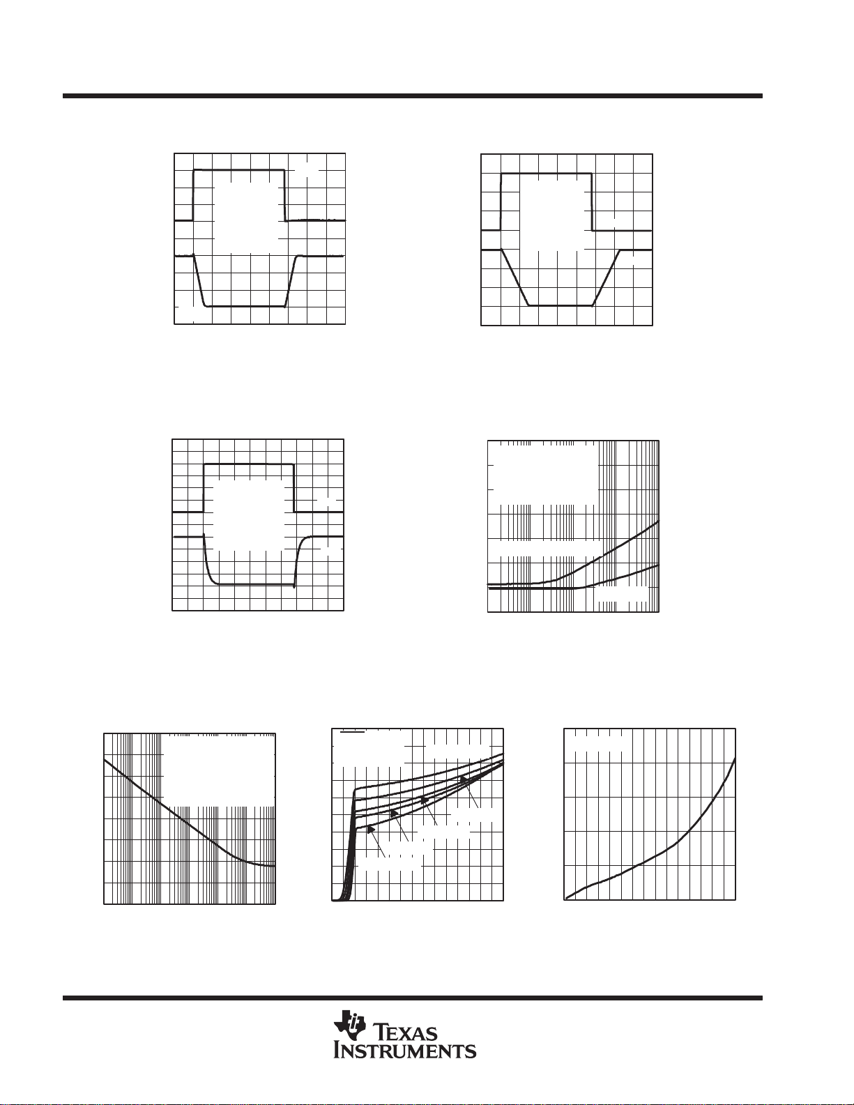
INVERTING LARGE-SIGNAL RESPONSE
INVERTING SMALL-SIGNAL RESPONSE
µ
SLOS270C − MARCH 2001 − REVISED DECEMBER 2003
TYPICAL CHARACTERISTICS
4
3
2
1
− Input Voltage − V
0
I
V
VDD = 5 V
AV = 1
RL = 2 kΩ
CL = 10 pF
VI = 3 V
TA = 25°C
V
O
2468
20
PP
t − Time − µs
Figure 24
0.10
0.05
− Input Voltage − VV
0
I
VDD = 5 V
AV = −1
RL = 2 kΩ
CL = 10 pF
VI = 100 mV
TA = 25°C
0 0.5 1 1.5 2 2.5 3 3.5 4 4.5
t − Time − µs
Figure 26
SHUTDOWN FORWARD AND
REVERSE ISOLATION
vs
FREQUENCY
160
140
120
100
80
60
40
20
0
Shutdown Forward and Reverse Isolation − dB
10 100 1 k 10 k 100 k 1 M 1 M
VDD = 2.7 V, 5 V & 15 V
VI = VDD /2
RL = 2 kΩ
CL= 10 pF
AV = 1
TA = 25°C
f − Frequency − Hz
Figure 28
V
I
10 12 14 16
V
I
pp
V
O
50
A/Chµ
45
40
35
30
25
20
15
− Shutdown Supply Current −
10
DD
I
5
0
0 1 2 3 4 5 6 7 8 9 1011 12 13 14 15
INVERTING LARGE-SIGNAL RESPONSE
12
9
6
3
− Input Voltage − VV
0
I
3
2
1
− Output Voltage − V
0
O
V
0
−20
−40
−60
0.1
0.05
0
− Output Voltage − VV
O
−80
−100
Crosstalk − dB
−120
−140
10 100 1 k 10 k 100 k
SHUTDOWN SUPPLY CURRENT
vs
SUPPLY VOLTAGE
SHDN = 0 V
VI = VDD/2
AV = 1
TA = 0°C
TA = −40°C
VDD − Supply Voltage − V
TA = 125°C
TA = 70°C
TA = 25°C
Figure 29
VDD = 15 V
AV = −1
RL = 2 kΩ
CL = 10 pF
VI = 9 V
pp
TA = 25°C
0246810121416
t − Time − µs
V
I
9
V
O
6
3
0
Figure 25
CROSSTALK
vs
FREQUENCY
VDD = 2.7, 5, & 15 V
VI = VDD/2
AV = 1
RL = 2 kΩ
TA = 25°C
Crosstalk in Shutdown
Crosstalk
f − Frequency −Hz
Figure 27
SHUTDOWN PIN LEAKAGE CURRENT
vs
SHUTDOWN PIN VOLTAGE
250
TA = 125°C
200
150
100
50
DD
I Shutdown Pin Leakage Current −−pA
0
0123456789101112131415
Shutdown Pin Voltage − V
Figure 30
− Output Voltage − VV
O
12
POST OFFICE BOX 1443
WWW.TI.COM
• HOUSTON, TEXAS 77251−1443
Page 13
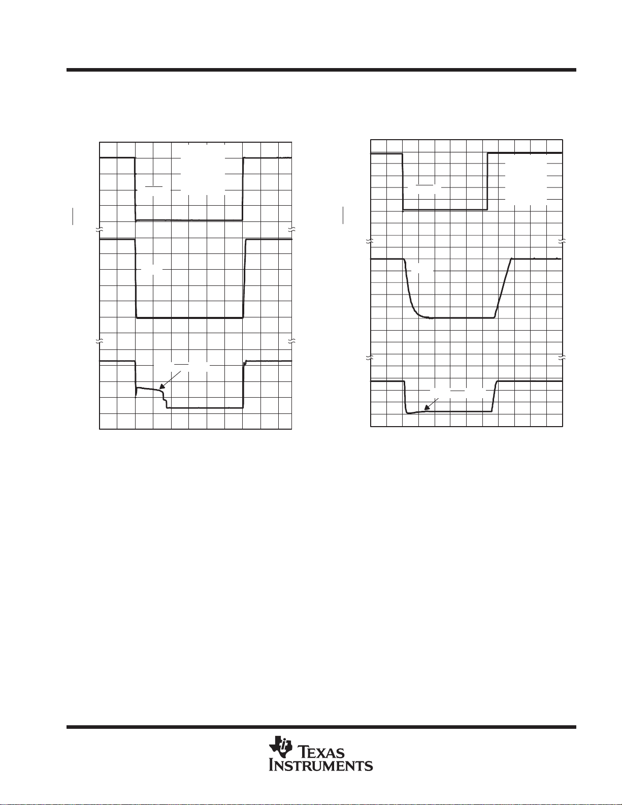
SHUTDOWN SUPPLY CURRENT/OUTPUT VOLTAGE
SHUTDOWN SUPPLY CURRENT/OUTPUT VOLTAGE
µ
SLOS270C − MARCH 2001 − REVISED DECEMBER 2003
TYPICAL CHARACTERISTICS
vs
TIME
10
8
6
4
2
0
SHDN − Shutdown Pulse − V
7.5
6
4.5
3
1.5
− Output Voltage − VV
O
0
−1.5
1
0.75
0.50
0.25
− Supply Current − mA/Ch
0
DD
I
−0.25
−40 −20 0 20 40 60 80 100 120 140 160
SHDN
V
O
VDD = 15 V
AV = 1
RL = 2 kΩ
CL = 10 pF
VI = VDD/2
TA = 25° C
I
DD(SHDN = 0)
t − Time − µs
vs
6
5
4
3
2
1
0
SHDN − Shutdown Pulse − V
2.5
2
1.5
1
− Output Voltage − VV
0.5
O
0
−0.5
−1.0
1
0.75
0.50
− Supply Current − mA/Ch
0.25
DD
I
0
−0.25
−2 −1 0 1 2 3 4 5 6 7 8 9 10
SHDN
V
O
TIME
I
DD(SHDN = 0)
t − Time − µs
VDD = 5 V
AV = 1
RL = 2 kΩ
CL = 10 pF
VI = VDD/2
TA = 25° C
Figure 31
Figure 32
POST OFFICE BOX 1443
WWW.TI.COM
• HOUSTON, TEXAS 77251−1443
13
Page 14
µ
SLOS270C − MARCH 2001 − REVISED DECEMBER 2003
APPLICATION INFORMATION
rail-to-rail input operation
The TLV237x input stage consists of two differential transistor pairs, NMOS and PMOS, that operate together
to achieve rail-to-rail input operation. The transition point between these two pairs can be seen in Figures 1,
2, and 3 for a 2.7-V , 5-V, and 15-V supply. As the common-mode input voltage approaches the positive supply
rail, the input pair switches from the PMOS differential pair to the NMOS differential pair. This transition occurs
approximately 1.35 V from the positive rail and results in a change in offset voltage due to different device
characteristics between the NMOS and PMOS pairs. If the input signal to the device is large enough to swing
between both rails, this transition results in a reduction in common-mode rejection ratio (CMRR). If the input
signal does not swing between both rails, it is best to bias the signal in the region where only one input pair is
active. This is the region in Figures 1 through 3 where the offset voltage varies slightly across the input range
and optimal CMRR can be achieved. This has the greatest impact when operating from a 2.7-V supply voltage.
driving a capacitive load
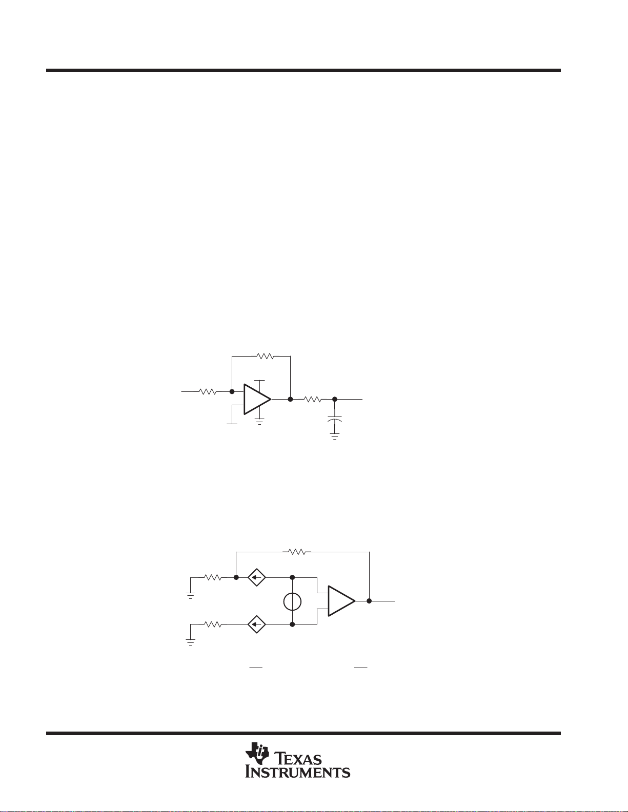
When the amplifier is configured in this manner , capacitive loading directly on the output decreases the device’ s
phase margin leading to high frequency ringing or oscillations. Therefore, for capacitive loads of greater than
10 pF, it is recommended that a resistor be placed in series (R
in Figure 33. A minimum value of 20 Ω should work well for most applications.
R
F
) with the output of the amplifier, as shown
NULL
R
Input
G
−
+
VDD/2
Figure 33. Driving a Capacitive Load
R
NULL
C
LOAD
Output
offset voltage
The output offset voltage, (VOO) is the sum of the input offset voltage (VIO) and both input bias currents (IIB) times
the corresponding gains. The following schematic and formula can be used to calculate the output offset
voltage:
R
F
I
VOO+ V
R
G
R
S
ǒ
IO
1 ) ǒ
IB−
+
V
I
I
IB+
R
F
Ǔ
" I
Ǔ
R
G
IB)
−
+
R
1 ) ǒ
F
Ǔ
R
G
R
ǒ
S
V
O
" I
Ǔ
IB–RF
14
Figure 34. Output Offset Voltage Model
POST OFFICE BOX 1443
WWW.TI.COM
• HOUSTON, TEXAS 77251−1443
Page 15
µ
SLOS270C − MARCH 2001 − REVISED DECEMBER 2003
APPLICATION INFORMATION
general configurations
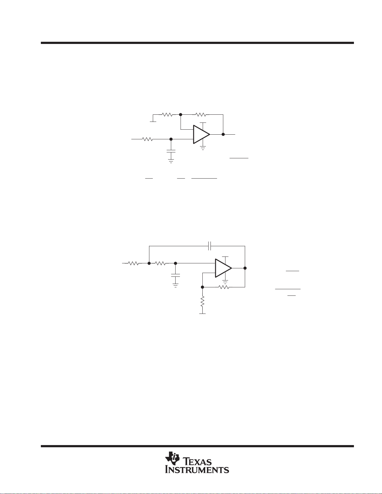
When receiving low-level signals, limiting the bandwidth of the incoming signals into the system is often
required. The simplest way to accomplish this is to place an RC filter at the noninverting terminal of the amplifier
(see Figure 35).
R
G
R
F
VDD/2
V
I
R1
V
O
+ ǒ1 )
V
I
C1
R
F
R
G
−
+
ǒ
Ǔ
1 ) sR1C1
f
1
–3dB
Ǔ
+
V
O
1
2pR1C1
Figure 35. Single-Pole Low-Pass Filter
If even more attenuation is needed, a multiple pole filter is required. The Sallen-Key filter can be used for this
task. For best results, the amplifier should have a bandwidth that is 8 to 10 times the filter frequency bandwidth.
Failure to do this can result in phase shift of the amplifier.
C1
V
I
R2R1
C2
R
G
+
_
R
F
R1 = R2 = R
C1 = C2 = C
Q = Peaking Factor
(Butterworth Q = 0.707)
1
+
2pRC
R
F
1
2 −
(
)
Q
R
f
–3dB
G
=
VDD/2
Figure 36. 2-Pole Low-Pass Sallen-Key Filter
POST OFFICE BOX 1443
WWW.TI.COM
• HOUSTON, TEXAS 77251−1443
15
Page 16

µ
SLOS270C − MARCH 2001 − REVISED DECEMBER 2003
APPLICATION INFORMATION
circuit layout considerations
To achieve the levels of high performance of the TLV237x, follow proper printed-circuit board design techniques.
A general set of guidelines is given in the following.
D Ground planes—It is highly recommended that a ground plane be used on the board to provide all
components with a low inductive ground connection. However, in the areas of the amplifier inputs and
output, the ground plane can be removed to minimize the stray capacitance.
D Proper power supply decoupling—Use a 6.8-µF tantalum capacitor in parallel with a 0.1-µF ceramic
capacitor on each supply terminal. It may be possible to share the tantalum among several amplifiers
depending on the application, but a 0.1-µF ceramic capacitor should always be used on the supply terminal
of every amplifier. In addition, the 0.1-µF capacitor should be placed as close as possible to the supply
terminal. As this distance increases, the inductance in the connecting trace makes the capacitor less
effective. The designer should strive for distances of less than 0.1 inches between the device power
terminals and the ceramic capacitors.
D Sockets—Sockets can be used but are not recommended. The additional lead inductance in the socket pins
will often lead to stability problems. Surface-mount packages soldered directly to the printed-circuit board
is the best implementation.
D Short trace runs/compact part placements—Optimum high performance is achieved when stray series
inductance has been minimized. To realize this, the circuit layout should be made as compact as possible,
thereby minimizing the length of all trace runs. Particular attention should be paid to the inverting input of
the amplifier. Its length should be kept as short as possible. This helps to minimize stray capacitance at the
input of the amplifier.
D Surface-mount passive components—Using surface-mount passive components is recommended for high
performance amplifier circuits for several reasons. First, because of the extremely low lead inductance of
surface-mount components, the problem with stray series inductance is greatly reduced. Second, the small
size of surface-mount components naturally leads to a more compact layout thereby minimizing both stray
inductance and capacitance. If leaded components are used, it is recommended that the lead lengths be
kept as short as possible.
shutdown function
Three members of the TLV237x family (TLV2370/3/5) have a shutdown terminal for conserving battery life in
portable applications. When the shutdown terminal is tied low, the supply current is reduced to 25 µA/channel,
the amplifier is disabled, and the outputs are placed in a high impedance mode. To enable the amplifier, the
shutdown terminal can either be left floating or pulled high. When the shutdown terminal is left floating, care
should be taken to ensure that parasitic leakage current at the shutdown terminal does not inadvertently place
the operational amplifier into shutdown.
16
POST OFFICE BOX 1443
WWW.TI.COM
• HOUSTON, TEXAS 77251−1443
Page 17
µ
SLOS270C − MARCH 2001 − REVISED DECEMBER 2003
APPLICATION INFORMATION
general power dissipation considerations
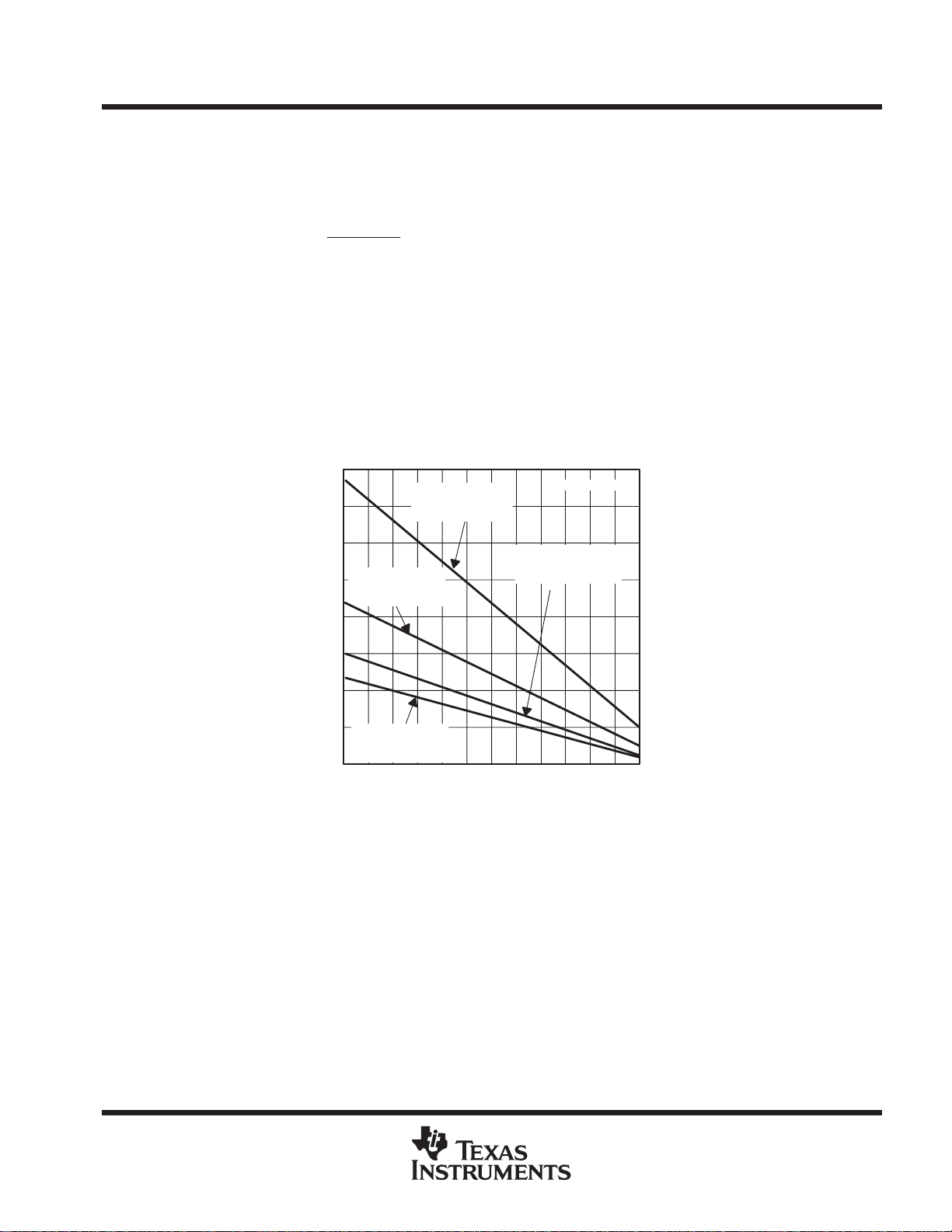
For a given θJA, the maximum power dissipation is shown in Figure 37 and is calculated by the following formula:
T
MAX–TA
Where:
ǒ
+
D
q
= Maximum power dissipation of TLV237x IC (watts)
= Absolute maximum junction temperature (150°C)
= Free-ambient air temperature (°C)
= θ
+ θ
JC
θ
= Thermal coefficient from junction to case
JC
θ
= Thermal coefficient from case to ambient air (°C/W)
CA
2
1.75
P
T
T
A
θ
JA
P
D
MAX
Ǔ
JA
CA
MAXIMUM POWER DISSIPATION
vs
FREE-AIR TEMPERATURE
PDIP Package
Low-K Test PCB
θJA = 104°C/W
TJ = 150°C
1.5
SOIC Package
1.25
Low-K Test PCB
θJA = 176°C/W
1
0.75
0.5
Maximum Power Dissipation − W
SOT-23 Package
0.25
Low-K Test PCB
θJA = 324°C/W
0
−55−40 −25 −10 5
TA − Free-Air Temperature − °C
NOTE A: Results are with no air flow and using JEDEC Standard Low-K test PCB.
20 35 50
MSOP Package
Low-K Test PCB
θJA = 260°C/W
65 80 95 110 125
Figure 37. Maximum Power Dissipation vs Free-Air Temperature
POST OFFICE BOX 1443
WWW.TI.COM
• HOUSTON, TEXAS 77251−1443
17
Page 18
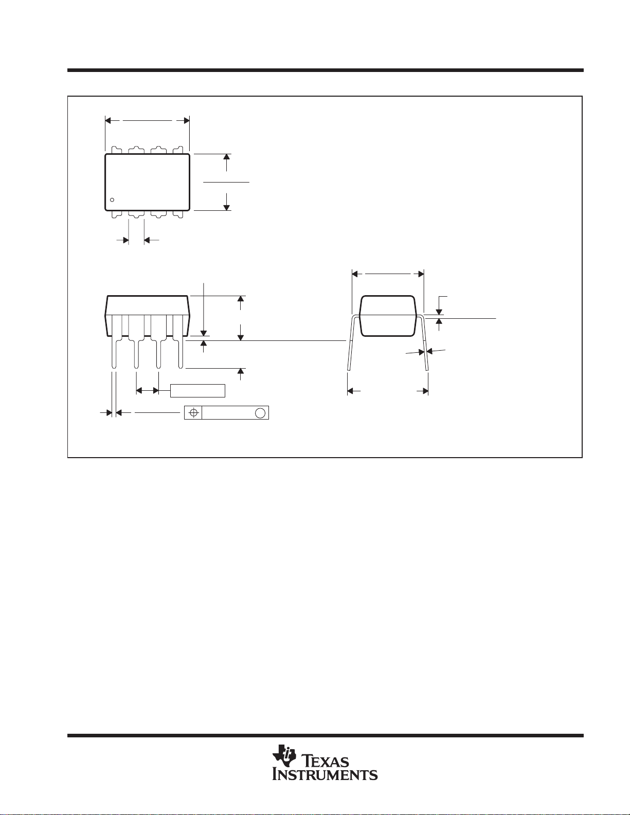
MECHANICAL DATA
MPDI001A – JANUARY 1995 – REVISED JUNE 1999
P (R-PDIP-T8) PLASTIC DUAL-IN-LINE
0.400 (10,60)
0.355 (9,02)
8
5
0.260 (6,60)
0.240 (6,10)
1
0.021 (0,53)
0.015 (0,38)
NOTES: A. All linear dimensions are in inches (millimeters).
B. This drawing is subject to change without notice.
C. Falls within JEDEC MS-001
4
0.070 (1,78) MAX
0.020 (0,51) MIN
0.200 (5,08) MAX
0.125 (3,18) MIN
0.100 (2,54)
0.010 (0,25)
Seating Plane
M
0.325 (8,26)
0.300 (7,62)
0.015 (0,38)
Gage Plane
0.010 (0,25) NOM
0.430 (10,92)
MAX
4040082/D 05/98
For the latest package information, go to http://www.ti.com/sc/docs/package/pkg_info.htm
POST OFFICE BOX 655303 • DALLAS, TEXAS 75265
Page 19
Page 20
Page 21
Page 22
Page 23
Page 24
Page 25
Page 26
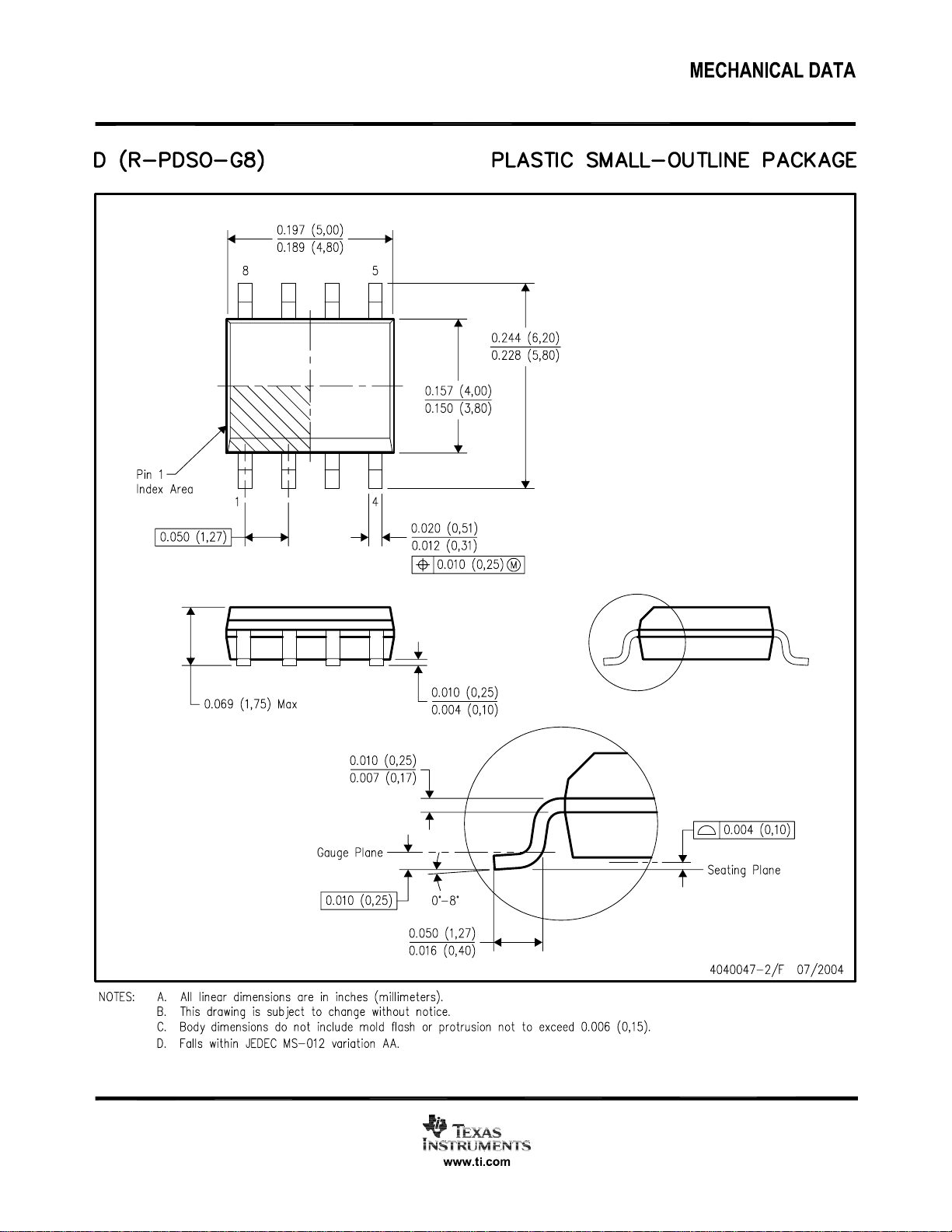
Page 27
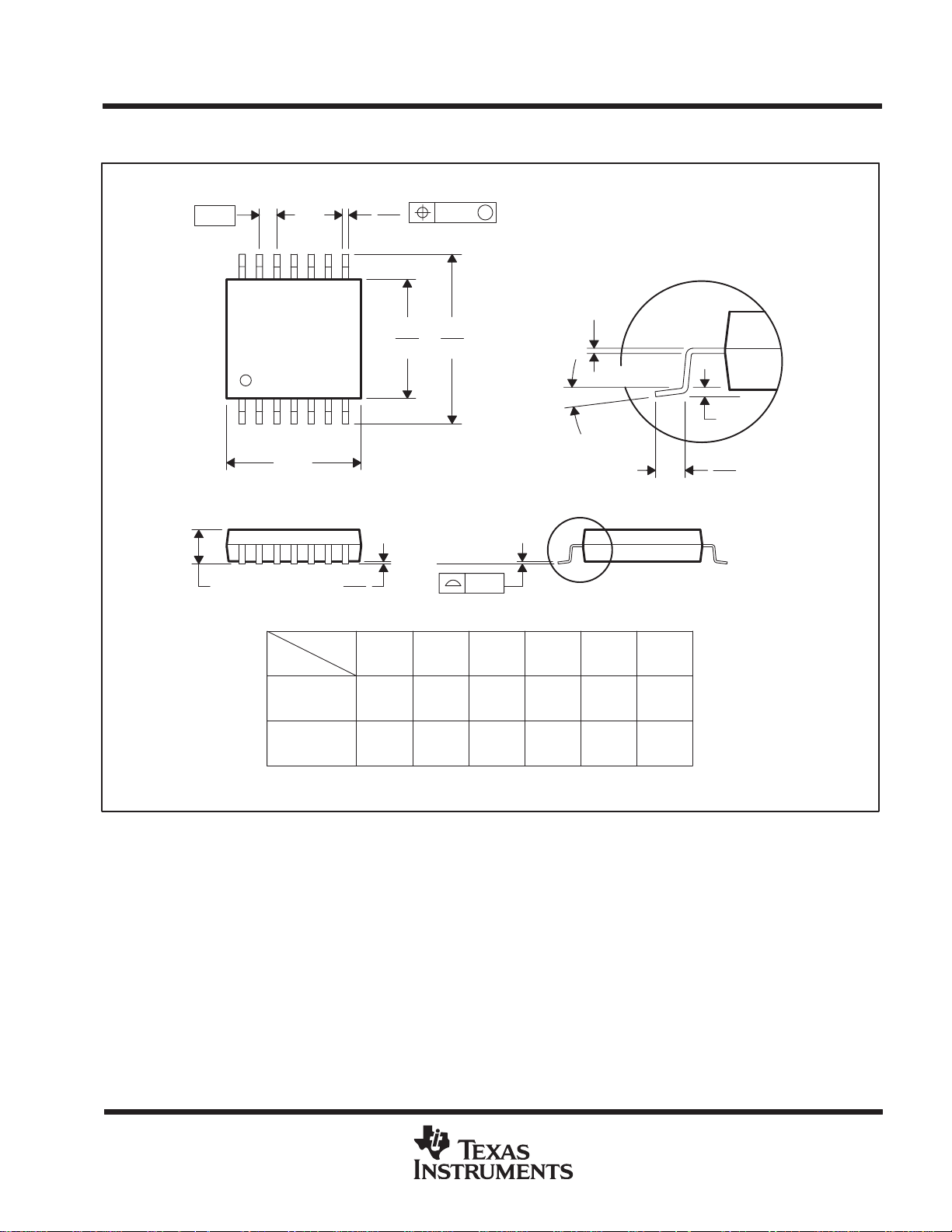
MECHANICAL DATA
MTSS001C – JANUARY 1995 – REVISED FEBRUARY 1999
PW (R-PDSO-G**) PLASTIC SMALL-OUTLINE PACKAGE
14 PINS SHOWN
0,65
1,20 MAX
14
0,30
0,19
8
4,50
4,30
PINS **
7
Seating Plane
0,15
0,05
8
1
A
DIM
14
0,10
6,60
6,20
M
0,10
0,15 NOM
0°–8°
2016
Gage Plane
24
0,25
0,75
0,50
28
A MAX
A MIN
NOTES: A. All linear dimensions are in millimeters.
B. This drawing is subject to change without notice.
C. Body dimensions do not include mold flash or protrusion not to exceed 0,15.
D. Falls within JEDEC MO-153
3,10
2,90
5,10
4,90
5,10
4,90
6,60
6,40
7,90
7,70
9,80
9,60
4040064/F 01/97
POST OFFICE BOX 655303 • DALLAS, TEXAS 75265
Page 28

IMPORTANT NOTICE
Texas Instruments Incorporated and its subsidiaries (TI) reserve the right to make corrections, modifications,
enhancements, improvements, and other changes to its products and services at any time and to discontinue
any product or service without notice. Customers should obtain the latest relevant information before placing
orders and should verify that such information is current and complete. All products are sold subject to TI’s terms
and conditions of sale supplied at the time of order acknowledgment.
TI warrants performance of its hardware products to the specifications applicable at the time of sale in
accordance with TI’s standard warranty. Testing and other quality control techniques are used to the extent TI
deems necessary to support this warranty . Except where mandated by government requirements, testing of all
parameters of each product is not necessarily performed.
TI assumes no liability for applications assistance or customer product design. Customers are responsible for
their products and applications using TI components. To minimize the risks associated with customer products
and applications, customers should provide adequate design and operating safeguards.
TI does not warrant or represent that any license, either express or implied, is granted under any TI patent right,
copyright, mask work right, or other TI intellectual property right relating to any combination, machine, or process
in which TI products or services are used. Information published by TI regarding third-party products or services
does not constitute a license from TI to use such products or services or a warranty or endorsement thereof.
Use of such information may require a license from a third party under the patents or other intellectual property
of the third party, or a license from TI under the patents or other intellectual property of TI.
Reproduction of information in TI data books or data sheets is permissible only if reproduction is without
alteration and is accompanied by all associated warranties, conditions, limitations, and notices. Reproduction
of this information with alteration is an unfair and deceptive business practice. TI is not responsible or liable for
such altered documentation.
Resale of TI products or services with statements different from or beyond the parameters stated by TI for that
product or service voids all express and any implied warranties for the associated TI product or service and
is an unfair and deceptive business practice. TI is not responsible or liable for any such statements.
Following are URLs where you can obtain information on other Texas Instruments products and application
solutions:
Products Applications
Amplifiers amplifier.ti.com Audio www.ti.com/audio
Data Converters dataconverter.ti.com Automotive www.ti.com/automotive
DSP dsp.ti.com Broadband www.ti.com/broadband
Interface interface.ti.com Digital Control www.ti.com/digitalcontrol
Logic logic.ti.com Military www.ti.com/military
Power Mgmt power.ti.com Optical Networking www.ti.com/opticalnetwork
Microcontrollers microcontroller.ti.com Security www.ti.com/security
Telephony www.ti.com/telephony
Video & Imaging www.ti.com/video
Wireless www.ti.com/wireless
Mailing Address: Texas Instruments
Post Office Box 655303 Dallas, Texas 75265
Copyright 2004, Texas Instruments Incorporated
 Loading...